EP1148552A2 - DRAM-Zelle mit vertikalem Transistor und Stapelkondensator und Herstellungsverfahren dafür - Google Patents
DRAM-Zelle mit vertikalem Transistor und Stapelkondensator und Herstellungsverfahren dafür Download PDFInfo
- Publication number
- EP1148552A2 EP1148552A2 EP01303617A EP01303617A EP1148552A2 EP 1148552 A2 EP1148552 A2 EP 1148552A2 EP 01303617 A EP01303617 A EP 01303617A EP 01303617 A EP01303617 A EP 01303617A EP 1148552 A2 EP1148552 A2 EP 1148552A2
- Authority
- EP
- European Patent Office
- Prior art keywords
- layer
- pillar
- adjacent
- source
- integrated circuit
- Prior art date
- Legal status (The legal status is an assumption and is not a legal conclusion. Google has not performed a legal analysis and makes no representation as to the accuracy of the status listed.)
- Withdrawn
Links
Images




Classifications
-
- H—ELECTRICITY
- H10—SEMICONDUCTOR DEVICES; ELECTRIC SOLID-STATE DEVICES NOT OTHERWISE PROVIDED FOR
- H10B—ELECTRONIC MEMORY DEVICES
- H10B12/00—Dynamic random access memory [DRAM] devices
- H10B12/30—DRAM devices comprising one-transistor - one-capacitor [1T-1C] memory cells
- H10B12/34—DRAM devices comprising one-transistor - one-capacitor [1T-1C] memory cells the transistor being at least partially in a trench in the substrate
-
- H—ELECTRICITY
- H10—SEMICONDUCTOR DEVICES; ELECTRIC SOLID-STATE DEVICES NOT OTHERWISE PROVIDED FOR
- H10D—INORGANIC ELECTRIC SEMICONDUCTOR DEVICES
- H10D30/00—Field-effect transistors [FET]
- H10D30/60—Insulated-gate field-effect transistors [IGFET]
- H10D30/63—Vertical IGFETs
-
- H—ELECTRICITY
- H10—SEMICONDUCTOR DEVICES; ELECTRIC SOLID-STATE DEVICES NOT OTHERWISE PROVIDED FOR
- H10B—ELECTRONIC MEMORY DEVICES
- H10B12/00—Dynamic random access memory [DRAM] devices
- H10B12/01—Manufacture or treatment
- H10B12/02—Manufacture or treatment for one transistor one-capacitor [1T-1C] memory cells
- H10B12/05—Making the transistor
- H10B12/053—Making the transistor the transistor being at least partially in a trench in the substrate
-
- H—ELECTRICITY
- H10—SEMICONDUCTOR DEVICES; ELECTRIC SOLID-STATE DEVICES NOT OTHERWISE PROVIDED FOR
- H10B—ELECTRONIC MEMORY DEVICES
- H10B12/00—Dynamic random access memory [DRAM] devices
- H10B12/30—DRAM devices comprising one-transistor - one-capacitor [1T-1C] memory cells
- H10B12/31—DRAM devices comprising one-transistor - one-capacitor [1T-1C] memory cells having a storage electrode stacked over the transistor
-
- H—ELECTRICITY
- H10—SEMICONDUCTOR DEVICES; ELECTRIC SOLID-STATE DEVICES NOT OTHERWISE PROVIDED FOR
- H10D—INORGANIC ELECTRIC SEMICONDUCTOR DEVICES
- H10D64/00—Electrodes of devices having potential barriers
- H10D64/20—Electrodes characterised by their shapes, relative sizes or dispositions
- H10D64/27—Electrodes not carrying the current to be rectified, amplified, oscillated or switched, e.g. gates
- H10D64/311—Gate electrodes for field-effect devices
- H10D64/411—Gate electrodes for field-effect devices for FETs
- H10D64/511—Gate electrodes for field-effect devices for FETs for IGFETs
- H10D64/512—Disposition of the gate electrodes, e.g. buried gates
Definitions
- the present invention relates to electronic circuits, and, more particularly, to integrated circuit memory devices and related methods.
- DRAM dynamic random access memory
- One approach to increase the density of a DRAM cell is to vertically stack the capacitor on the access transistor.
- the result is a memory cell that takes up less horizontal area and allows more memory cells to be included on a chip.
- the stacked arrangement can also be used with a vertical channel access transistor to reduce the size of each cell, as disclosed, for example, in U.S. Patent No. 5,885,864 to Ma entitled "Method for Forming Compact Memory Cell Using Vertical Devices.”
- a cylindrical stacked storage capacitor is used to provide sufficient capacitance in a relatively small area.
- the vertical channel access transistor may be difficult to make while providing a controllable and consistent channel.
- the cylindrical capacitor structure may also be relatively complicated and difficult to scale upward for increased capacitance.
- an integrated circuit memory device including a substrate having at least one connection line therein and a plurality of memory cells formed on the substrate.
- Each memory cell includes a pillar which may be formed of epitaxial silicon.
- the pillar includes a lower source/drain region for the cell access transistor and which is electrically connected to the at least one connection line in the substrate.
- the pillar also includes an upper source/drain region for the cell access transistor, and at least one channel region extending vertically between the lower source/drain region and the upper source/drain region.
- the pillar may be generally cylindrical or rectangular in shape.
- Each memory cell may further include at least one lower dielectric layer vertically adjacent the substrate and laterally adjacent the pillar, and at least one upper dielectric layer vertically spaced above the at least one lower dielectric layer and laterally adjacent the pillar. Also included is at least one gate for the channel of the cell access transistor between the lower and upper dielectric layers so that the vertical spacing therebetween defines a gate length for the cell access transistor. The construction of the vertical channel access transistor permits accurate control of the length of the channel.
- a storage capacitor is included in each memory cell adjacent the upper source/drain region of the cell access transistor and is electrically connected thereto.
- a conductive source/drain layer may be provided between the upper source/drain region of the pillar and the storage capacitor.
- the conductive source/drain layer has an upper surface portion and vertical sidewall portions depending therefrom.
- An advantageous feature of the invention is that the storage capacitor may extend adjacent the upper surface portion and also adjacent the vertical sidewall portions of the conductive source/drain layer to thereby provide increased area for the storage capacitor.
- the conductive source/drain layer can be extended vertically relatively easily to provide a relatively high capacitance, since the vertical sidewalls can be made relatively large. This is so even as the horizontal area of each cell is scaled downward.
- At least one dielectric spacer may be provided adjacent the vertical sidewall portions of the conductive source/drain layer.
- the storage capacitor may comprise a first electrode layer adjacent the upper source/drain region of the pillar that is electrically connected thereto, a dielectric layer adjacent the first electrode layer, and a second electrode layer adjacent the dielectric layer.
- connection line may be provided by a doped substrate region, and the strapping may be metal to thus lower an effective electrical resistance of the doped substrate region.
- a method aspect of the present invention is for making an integrated circuit memory device.
- the method includes forming at least one connection line in a substrate and forming a pillar on the connection line.
- the pillar includes a lower source/drain region for a cell access transistor electrically connected to the at least one connection line, an upper source/drain region for the cell access transistor, and at least one channel region extending vertically between the lower source/drain region and the upper source/drain region
- the method further includes forming at least one lower dielectric layer vertically adjacent the substrate and laterally adjacent the pillar and forming at least one upper dielectric layer vertically spaced above the at least one lower dielectric layer and laterally adjacent the pillar.
- At least one gate is formed for the at least one channel of the cell access transistor between the lower and upper dielectric layers so that the vertical spacing therebetween defines a gate length for the cell access transistor.
- a capacitor is formed adjacent the upper source/drain region of the cell access transistor and electrically connected thereto.
- FIG. 1 is a cross-sectional view of a memory cell according to the present invention.
- FIG. 2 is a cross-sectional view showing the formation of the connection line in the substrate of the memory cell of FIG. 1.
- FIG. 3 is a cross-sectional view showing the formation of the upper and lower dielectric layers of the memory cell of FIG. 1 along with a sacrificial gate layer.
- FIG. 4 is a cross-sectional view showing the formation of a window in the dielectric layers of FIG. 3.
- FIG. 5 is a cross-sectional view showing the formation of the pillar of the memory cell of FIG. 1.
- FIG. 6 is a cross-sectional view showing the formation of the conductive source/drain layer of the memory cell of FIG. 1.
- FIG. 7 is a cross-sectional view showing patterning of the upper dielectric layer and the conductive source/drain layer and the formation of the dielectric spacer of the memory cell of FIG. 1.
- FIG. 8 is a cross-sectional view showing the removal of the sacrificial gate layer shown in FIGS. 3 through 7.
- FIG. 9 is a cross-sectional view showing the formation of the gate oxide and conductive gate layers of the memory cell of FIG. 1.
- FIG. 10. is a cross-sectional view of an alternative embodiment of the memory cell of FIG. 1.
- FIG. 11 is an elevational cross-sectional view of the memory cell of FIG. 1 having a generally cylindrical lpillar shown after removal of the sacrificial gate layer.
- FIG. 12 is a elevational cross-sectional view of an alternate embodiment of the memory cell of FIG. 1 having a generally rectangular pillar shown after removal of the sacrificial gate layer.
- FIG. 13 is a cross-sectional view of a memory device including memory cells in accordance with the present invention.
- a memory cell 20 of an integrated circuit memory device is first described with reference to FIG. 1.
- the memory cell 20 includes a semiconductor substrate 22 having at least one connection line 23 therein.
- a pillar 40 has a lower source/drain region 42 electrically connected to the at least one connection line 23, an upper source/drain region 44, and at least one channel region 46 extending vertically between the lower source/drain region and the upper source/drain region.
- a conductive source/drain layer 48 is vertically adjacent the upper source/drain region 23 of the pillar 40.
- the conductive source/drain layer 48 has an upper surface portion and vertical sidewall portions depending therefrom, and at least one dielectric spacer 50 is formed adjacent the upper surface and vertical sidewall portions.
- At least one lower dielectric layer illustratively includes in stacked relation: a first oxide layer 24, a second oxide layer 26 on the first oxide layer, and a silicon nitride layer 28 on the second oxide layer.
- the at least one lower dielectric layer is vertically adjacent the substrate 22 and laterally adjacent the pillar 40.
- At least one upper dielectric layer illustratively includes in stacked relation: a first silicone nitride layer 55, an oxide layer 26 on the first silicone nitride layer, and a second silicon nitride layer 38 on the oxide layer.
- the at least one upper dielectric layer is vertically above the at least one lower dielectric layer and laterally adjacent the pillar 40.
- At least one gate is positioned between the at least one lower dielectric layer and the at least one upper dielectric layer and illustratively includes a conductive gate layer 52 and a gate oxide layer 51 between the conductive gate layer and adjacent portions of the pillar 40.
- This cell access transistor is similar to a vertical metal-oxide semiconductor field-effect transistor (MOSFET) assigned to the assignee of the present invention and disclosed in U.S. Patent No. 6,027,975 to Hergenrother et al. entitled “Process for Fabricating Vertical Transistors,” which is hereby incorporated herein by reference in its entirety.
- MOSFET vertical metal-oxide semiconductor field-effect transistor
- the structure of the cell access transistor and its fabrication will be described below. However, further details regarding this vertical MOSFET and its fabrication can be found in the noted patent.
- the present invention may incorporate other embodiments of the vertical MOSFET disclosed in U.S. Patent NO. 6,027,975 and is not limited to the single embodiment described herein.
- the memory cell 20 also includes a storage capacitor adjacent the upper source/drain region 44 of the cell access transistor that is electrically connected thereto.
- the storage capacitor includes a first electrode layer 56 adjacent the upper source/drain region 44 and which is electrically connected thereto by the conductive source/drain layer 48.
- a dielectric layer 58 is adjacent the first electrode layer 56, and a second electrode layer 60 is adjacent the dielectric layer. This arrangement provides increased area by vertically extending the storage capacitor.
- a portion of the semiconductor substrate 22 may be degeneratively doped to form at least one connection line 23 therein for the memory cell 20, as shown in FIG. 2.
- the doping may be accomplished by ion implantation or other doping techniques as will be readily appreciated by those skilled in the art.
- a first oxide layer 24 may be formed on the substrate 22 and connection line 23, as shown in FIG. 3, using conventional techniques as will be appreciated by those skilled in the art. At least one lower dielectric layer 25 is then illustratively formed, such as by depositing a second oxide layer 26 on top of the first oxide layer 24, and then depositing or forming a silicon nitride layer 28 on the second oxide layer 26.
- a sacrificial gate layer 30 may be formed on the silicon nitride layer 28.
- the sacrificial gate layer 30 is preferably an oxide layer.
- At least one upper dielectric layer 32 is then illustratively formed, such as by depositing or forming a first silicone nitride layer 34 on the sacrificial gate layer 30, an oxide layer 36 on the first silicon nitride layer 34, and a second silicon nitride layer 38 on the oxide layer.
- a window 39 is etched starting at the silicon nitride layer 38 and extending down to the connection line 23, as shown in FIG. 4.
- the window 39 may be formed using conventional lithographic techniques as will be appreciated by those skilled in the art.
- a pillar 40 is then formed in the window 39 of a single crystal semiconducting material, such as epitaxial silicon, as seen in FIG. 5.
- the pillar 40 is then doped so as to define the lower and upper source/drain regions 42 and 44, respectively, and a channel region 46, which are illustrated with dotted lines.
- the doping is further described in the above cited patent to Hergenrother et al.
- a conductive source/drain layer 48 is formed on top of the silicon nitride layer 38 and the upper source/drain region 44, as shown in FIG. 6.
- the conductive source/drain layer 48 may be formed of polysilicon or other suitable materials known in the art.
- the conductive source/drain layer 48, the silicon nitride layer 38, and the oxide layer 36 are then patterned on either side of the pillar 30, as shown in FIG. 7. The patterning is accomplished through conventional lithographic techniques.
- a dielectric layer 50 is formed which will provide a dielectric spacer.
- the dielectric spacer 50 may also be silicon nitride.
- An anisotropic etchant such as a dry plasma etch, may be used to remove portions of the dielectric layer 50 and silicon nitride layer 34, thus exposing the sacrificial gate layer 30, which can then be removed, as shown in FIG. 8.
- the sacrificial gate layer is removed by etching such as, for example, by wet etching (e.g., aqueous hydrofluoric acid) or isotropic dry etching (e.g., anhydrous hydrofluoric acid).
- a gate oxide layer 51 is then formed about the pillar 40 in the space formerly occupied by the sacrificial gate layer 30, as shown in FIG. 9.
- a conductive gate layer 52 is then formed adjacent the gate oxide layer 51 and in the space formerly occupied by the sacrificial gate layer 30.
- separate conductive gate layers could be formed instead of the single conductive gate layer 52.
- a silicon nitride layer 55 may then be added to the top of the conductive gate layer 52 so as to contact the dielectric spacer 50, as seen in FIG. 1.
- the storage capacitor of the memory cell 20 is then formed by depositing a first electrode layer 56 on the dielectric spacer 50 and the silicon nitride layer 55.
- a dielectric layer 58 is then formed on the first electrode layer 56, and a second electrode layer 60 is formed on the dielectric layer 58, thus completing the storage capacitor.
- the first and second electrode layers 56, 60 are shown to be metal in FIG. 1; however, other suitable conductive materials known to those skilled in the art would also suffice.
- the dielectric spacer 50 is preferably generally rounded on its top portion so that it tapers toward the upper surface of the conductive source/drain layer 48. As such, the dielectric spacer 50 provides a smooth arc for the first electrode layer 56 to be formed over and also provides increased area for the storage capacitor. Also, the dielectric spacer 50 prevents the formation of sharp angles in the storage capacitor, making the storage capacitor less susceptible to current leakage. However, the dielectric spacer 50 need not extend fully to the upper surface of the conductive source/drain layer 38 and over the silicon nitride layer 49. Further, separate dielectric spacers could be formed instead of the single dielectric spacer 50.
- the capacitance of the storage capacitor can be adjusted by increasing or decreasing the height of the conductive source/drain layer 48.
- An alternate embodiment of the memory cell 20' is shown in FIG. 10.
- the conductive source/drain layer 48' has been vertically extended, resulting in a corresponding extension in the first and second electrode layers 56', 60' and the dielectric layer 58' of the storage capacitor.
- Such a vertical extension can be formed relatively easily and provides a relatively high capacitance to the storage capacitor of memory cell 20' .
- the other elements of the memory cell 20' are similar to those already described above and need no further discussion herein.
- the shape of the window 39 and, correspondingly, the shape of the pillar 40 may be generally cylindrical, as shown in FIG. 11.
- the pillar 40 " can be formed in a generally rectangular shape, as shown in FIG. 12.
- FIG. 12 those skilled in the art will appreciate that other geometries are also possible for the pillar 40, 40 ".
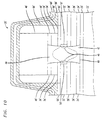
- a memory device 70 according to the present invention is shown in FIG. 13.
- the memory device 70 includes a plurality of memory cells 20 formed on the connection line 23 of the memory device, thereby defining a memory array.
- An electrically conductive line 74 is intermittently connected to the connection line 23 to lower an effective resistivity thereof.
- the electrically conductive line 74 may be metal although other suitable conductive materials would suffice.
Landscapes
- Engineering & Computer Science (AREA)
- Manufacturing & Machinery (AREA)
- Semiconductor Memories (AREA)
- Thin Film Transistor (AREA)
Applications Claiming Priority (2)
| Application Number | Priority Date | Filing Date | Title |
|---|---|---|---|
| US553868 | 2000-04-20 | ||
| US09/553,868 US6603168B1 (en) | 2000-04-20 | 2000-04-20 | Vertical DRAM device with channel access transistor and stacked storage capacitor and associated method |
Publications (2)
| Publication Number | Publication Date |
|---|---|
| EP1148552A2 true EP1148552A2 (de) | 2001-10-24 |
| EP1148552A3 EP1148552A3 (de) | 2005-10-12 |
Family
ID=24211094
Family Applications (1)
| Application Number | Title | Priority Date | Filing Date |
|---|---|---|---|
| EP01303617A Withdrawn EP1148552A3 (de) | 2000-04-20 | 2001-04-20 | DRAM-Zelle mit vertikalem Transistor und Stapelkondensator und Herstellungsverfahren dafür |
Country Status (5)
| Country | Link |
|---|---|
| US (1) | US6603168B1 (de) |
| EP (1) | EP1148552A3 (de) |
| JP (2) | JP2001308203A (de) |
| KR (1) | KR100757697B1 (de) |
| TW (1) | TW490840B (de) |
Cited By (2)
| Publication number | Priority date | Publication date | Assignee | Title |
|---|---|---|---|---|
| EP2256815A3 (de) * | 2009-05-29 | 2011-08-17 | Unisantis Electronics (Japan) Ltd. | Halbleiterbauelement mit umschliessendem Gate |
| TWI740552B (zh) * | 2012-05-10 | 2021-09-21 | 日商半導體能源研究所股份有限公司 | 半導體裝置 |
Families Citing this family (13)
| Publication number | Priority date | Publication date | Assignee | Title |
|---|---|---|---|---|
| US6706603B2 (en) * | 2001-02-23 | 2004-03-16 | Agere Systems Inc. | Method of forming a semiconductor device |
| US6478231B1 (en) * | 2001-06-29 | 2002-11-12 | Hewlett Packard Company | Methods for reducing the number of interconnects to the PIRM memory module |
| US20030052365A1 (en) * | 2001-09-18 | 2003-03-20 | Samir Chaudhry | Structure and fabrication method for capacitors integratible with vertical replacement gate transistors |
| US7372091B2 (en) * | 2004-01-27 | 2008-05-13 | Micron Technology, Inc. | Selective epitaxy vertical integrated circuit components |
| JP4164452B2 (ja) * | 2004-02-02 | 2008-10-15 | キヤノン株式会社 | 情報処理方法及び装置 |
| US7504685B2 (en) * | 2005-06-28 | 2009-03-17 | Micron Technology, Inc. | Oxide epitaxial isolation |
| JP5525156B2 (ja) * | 2008-12-09 | 2014-06-18 | ピーエスフォー ルクスコ エスエイアールエル | 半導体装置、および該半導体装置の製造方法 |
| US9177872B2 (en) | 2011-09-16 | 2015-11-03 | Micron Technology, Inc. | Memory cells, semiconductor devices, systems including such cells, and methods of fabrication |
| US9698261B2 (en) | 2014-06-30 | 2017-07-04 | Taiwan Semiconductor Manufacturing Co., Ltd. | Vertical device architecture |
| US9911848B2 (en) * | 2014-08-29 | 2018-03-06 | Taiwan Semiconductor Manufacturing Co., Ltd. | Vertical transistor and method of manufacturing the same |
| CN108538839B (zh) * | 2017-03-01 | 2019-08-23 | 联华电子股份有限公司 | 半导体结构、用于存储器元件的半导体结构及其制作方法 |
| JP2021153082A (ja) * | 2020-03-24 | 2021-09-30 | キオクシア株式会社 | 半導体装置及び半導体記憶装置 |
| CN118235532A (zh) | 2021-11-09 | 2024-06-21 | 新加坡优尼山帝斯电子私人有限公司 | 半导体内存装置及半导体内存装置的制造方法 |
Citations (1)
| Publication number | Priority date | Publication date | Assignee | Title |
|---|---|---|---|---|
| US5270239A (en) | 1991-08-21 | 1993-12-14 | Hyundai Electronics Industries Co., Ltd. | Method for manufacturing a dynamic random access memory cell |
Family Cites Families (22)
| Publication number | Priority date | Publication date | Assignee | Title |
|---|---|---|---|---|
| US4554570A (en) * | 1982-06-24 | 1985-11-19 | Rca Corporation | Vertically integrated IGFET device |
| JPH0793365B2 (ja) * | 1984-09-11 | 1995-10-09 | 株式会社東芝 | 半導体記憶装置およびその製造方法 |
| US5140389A (en) | 1988-01-08 | 1992-08-18 | Hitachi, Ltd. | Semiconductor memory device having stacked capacitor cells |
| JP2941039B2 (ja) * | 1990-11-08 | 1999-08-25 | 沖電気工業株式会社 | 半導体メモリ装置の製造方法 |
| JPH04188869A (ja) * | 1990-11-22 | 1992-07-07 | Mitsubishi Electric Corp | 接合型電界効果トランジスタとキャパシタとを含む半導体記憶装置およびその製造方法 |
| US5208172A (en) * | 1992-03-02 | 1993-05-04 | Motorola, Inc. | Method for forming a raised vertical transistor |
| US5234856A (en) | 1992-04-15 | 1993-08-10 | Micron Technology, Inc. | Dynamic random access memory cell having a stacked-trench capacitor that is resistant to alpha particle generated soft errors, and method of manufacturing same |
| US5335138A (en) | 1993-02-12 | 1994-08-02 | Micron Semiconductor, Inc. | High dielectric constant capacitor and method of manufacture |
| JPH06260610A (ja) * | 1993-03-02 | 1994-09-16 | Toshiba Corp | 半導体記憶装置及びその製造方法 |
| JP3403231B2 (ja) * | 1993-05-12 | 2003-05-06 | 三菱電機株式会社 | 半導体装置およびその製造方法 |
| JP3197134B2 (ja) * | 1994-01-18 | 2001-08-13 | 株式会社東芝 | 半導体装置 |
| KR0135803B1 (ko) | 1994-05-13 | 1998-04-24 | 김광호 | 상.하로 분리된 커패시터를 갖는 반도체 메모리장치 및 그 제조방법 |
| JP3745392B2 (ja) * | 1994-05-26 | 2006-02-15 | 株式会社ルネサステクノロジ | 半導体装置 |
| US5885882A (en) | 1995-07-18 | 1999-03-23 | Micron Technology, Inc. | Method for making polysilicon electrode with increased surface area making same |
| US5668036A (en) | 1996-06-21 | 1997-09-16 | Vanguard International Semiconductor Corporation | Fabrication method of the post structure of the cell for high density DRAM |
| US5712813A (en) | 1996-10-17 | 1998-01-27 | Zhang; Guobiao | Multi-level storage capacitor structure with improved memory density |
| KR19980028402A (ko) * | 1996-10-22 | 1998-07-15 | 문정환 | 디램(dram) 셀의 구조 및 그 제조 방법 |
| US5885864A (en) | 1996-10-24 | 1999-03-23 | Micron Technology, Inc. | Method for forming compact memory cell using vertical devices |
| US5824582A (en) | 1997-06-04 | 1998-10-20 | Vanguard International Semiconductor Corporation | Stack DRAM cell manufacturing process with high capacitance capacitor |
| US5909618A (en) | 1997-07-08 | 1999-06-01 | Micron Technology, Inc. | Method of making memory cell with vertical transistor and buried word and body lines |
| US6078072A (en) * | 1997-10-01 | 2000-06-20 | Mitsubishi Denki Kabushiki Kaisha | Semiconductor device having a capacitor |
| US6027975A (en) * | 1998-08-28 | 2000-02-22 | Lucent Technologies Inc. | Process for fabricating vertical transistors |
-
2000
- 2000-04-20 US US09/553,868 patent/US6603168B1/en not_active Expired - Lifetime
-
2001
- 2001-04-19 KR KR1020010021021A patent/KR100757697B1/ko not_active Expired - Fee Related
- 2001-04-19 TW TW090109388A patent/TW490840B/zh not_active IP Right Cessation
- 2001-04-20 EP EP01303617A patent/EP1148552A3/de not_active Withdrawn
- 2001-04-20 JP JP2001122417A patent/JP2001308203A/ja active Pending
-
2007
- 2007-09-19 JP JP2007241699A patent/JP4888975B2/ja not_active Expired - Fee Related
Patent Citations (1)
| Publication number | Priority date | Publication date | Assignee | Title |
|---|---|---|---|---|
| US5270239A (en) | 1991-08-21 | 1993-12-14 | Hyundai Electronics Industries Co., Ltd. | Method for manufacturing a dynamic random access memory cell |
Cited By (6)
| Publication number | Priority date | Publication date | Assignee | Title |
|---|---|---|---|---|
| EP2256815A3 (de) * | 2009-05-29 | 2011-08-17 | Unisantis Electronics (Japan) Ltd. | Halbleiterbauelement mit umschliessendem Gate |
| US8502303B2 (en) | 2009-05-29 | 2013-08-06 | Unisantis Electronics Singapore Pte Ltd. | Semiconductor device |
| US8860128B2 (en) | 2009-05-29 | 2014-10-14 | Unisantis Electronics Singapore Pte Ltd. | Semiconductor device having a surround gate transistor |
| US9076767B2 (en) | 2009-05-29 | 2015-07-07 | Unisantis Electronics Singapore Pte Ltd. | Semiconductor device having a surround gate transistor |
| TWI740552B (zh) * | 2012-05-10 | 2021-09-21 | 日商半導體能源研究所股份有限公司 | 半導體裝置 |
| TWI777675B (zh) * | 2012-05-10 | 2022-09-11 | 日商半導體能源研究所股份有限公司 | 半導體裝置 |
Also Published As
| Publication number | Publication date |
|---|---|
| TW490840B (en) | 2002-06-11 |
| KR20010098730A (ko) | 2001-11-08 |
| JP2008047933A (ja) | 2008-02-28 |
| JP2001308203A (ja) | 2001-11-02 |
| KR100757697B1 (ko) | 2007-09-13 |
| EP1148552A3 (de) | 2005-10-12 |
| JP4888975B2 (ja) | 2012-02-29 |
| US6603168B1 (en) | 2003-08-05 |
Similar Documents
| Publication | Publication Date | Title |
|---|---|---|
| JP4888975B2 (ja) | チャネルアクセストランジスタおよび積層型蓄積キャパシタを備えた垂直dram装置および関連方法 | |
| US8546215B2 (en) | Methods of fabricating a memory device | |
| US5716884A (en) | Process for fabricating a stacked capacitor | |
| KR960043226A (ko) | 디램 셀(dram) 및 그 제조 방법 | |
| CN1716610A (zh) | 双栅极鳍型场效应晶体管增益单元及其制造方法 | |
| TW202133390A (zh) | 記憶體結構及其製造方法 | |
| WO2006012114A1 (en) | Methods for forming semiconductor wires and resulting devices | |
| KR20030080234A (ko) | 트렌치 커패시터 및 그 제조 방법 | |
| CN100373623C (zh) | 动态随机存取存储单元和其阵列、及该阵列的制造方法 | |
| KR100572382B1 (ko) | 반도체 장치의 커패시터 및 이의 제조 방법 | |
| US20070134871A1 (en) | Memory chip having a memory cell with low-temperature layers in the memory trench and fabrication method | |
| US6518613B2 (en) | Memory cell configuration with capacitor on opposite surface of substrate and method for fabricating the same | |
| US5701264A (en) | Dynamic random access memory cell having increased capacitance | |
| CN116801613B (zh) | 半导体器件及其制作方法 | |
| JP2553995B2 (ja) | Dramセルの製造方法 | |
| US5783848A (en) | Memory cell | |
| JP3685997B2 (ja) | 集積回路装置に適した凹部を備えた基板及びその製造方法 | |
| TW410440B (en) | Manufacturing method for crown type capacitor of dynamic random access memory | |
| US5902123A (en) | Method of fabricating a stacked capacitor of a dynamic random access memory | |
| JP2653683B2 (ja) | 半導体トレンチ・メモリ・セル構造 | |
| TW293175B (en) | Stack capacitor of FIN structure for DRAM cell | |
| KR100369484B1 (ko) | 반도체 소자의 캐패시터 제조방법 | |
| KR100190524B1 (ko) | 반도체 소자의 전하 저장전극의 제조방법 | |
| CN121751631A (zh) | 包括电容器的存储器器件结构 | |
| KR100365419B1 (ko) | 반도체소자의캐패시터제조방법 |
Legal Events
| Date | Code | Title | Description |
|---|---|---|---|
| PUAI | Public reference made under article 153(3) epc to a published international application that has entered the european phase |
Free format text: ORIGINAL CODE: 0009012 |
|
| AK | Designated contracting states |
Kind code of ref document: A2 Designated state(s): AT BE CH CY DE DK ES FI FR GB GR IE IT LI LU MC NL PT SE TR |
|
| AX | Request for extension of the european patent |
Free format text: AL;LT;LV;MK;RO;SI |
|
| PUAL | Search report despatched |
Free format text: ORIGINAL CODE: 0009013 |
|
| AK | Designated contracting states |
Kind code of ref document: A3 Designated state(s): AT BE CH CY DE DK ES FI FR GB GR IE IT LI LU MC NL PT SE TR |
|
| AX | Request for extension of the european patent |
Extension state: AL LT LV MK RO SI |
|
| 17P | Request for examination filed |
Effective date: 20060317 |
|
| AKX | Designation fees paid |
Designated state(s): GB |
|
| 17Q | First examination report despatched |
Effective date: 20090929 |
|
| RAP1 | Party data changed (applicant data changed or rights of an application transferred) |
Owner name: AVAGO TECHNOLOGIES GENERAL IP (SINGAPORE) PTE. LTD |
|
| STAA | Information on the status of an ep patent application or granted ep patent |
Free format text: STATUS: EXAMINATION IS IN PROGRESS |
|
| STAA | Information on the status of an ep patent application or granted ep patent |
Free format text: STATUS: THE APPLICATION IS DEEMED TO BE WITHDRAWN |
|
| 18D | Application deemed to be withdrawn |
Effective date: 20171103 |