EP1148614A2 - Circuit de puissance alimenté par batterie et méthode de commande de cêlui-ci - Google Patents
Circuit de puissance alimenté par batterie et méthode de commande de cêlui-ci Download PDFInfo
- Publication number
- EP1148614A2 EP1148614A2 EP01109542A EP01109542A EP1148614A2 EP 1148614 A2 EP1148614 A2 EP 1148614A2 EP 01109542 A EP01109542 A EP 01109542A EP 01109542 A EP01109542 A EP 01109542A EP 1148614 A2 EP1148614 A2 EP 1148614A2
- Authority
- EP
- European Patent Office
- Prior art keywords
- switching device
- terminal
- current control
- control device
- power circuit
- Prior art date
- Legal status (The legal status is an assumption and is not a legal conclusion. Google has not performed a legal analysis and makes no representation as to the accuracy of the status listed.)
- Withdrawn
Links
Images




Classifications
-
- H—ELECTRICITY
- H02—GENERATION; CONVERSION OR DISTRIBUTION OF ELECTRIC POWER
- H02M—APPARATUS FOR CONVERSION BETWEEN AC AND AC, BETWEEN AC AND DC, OR BETWEEN DC AND DC, AND FOR USE WITH MAINS OR SIMILAR POWER SUPPLY SYSTEMS; CONVERSION OF DC OR AC INPUT POWER INTO SURGE OUTPUT POWER; CONTROL OR REGULATION THEREOF
- H02M3/00—Conversion of DC power input into DC power output
- H02M3/02—Conversion of DC power input into DC power output without intermediate conversion into AC
- H02M3/04—Conversion of DC power input into DC power output without intermediate conversion into AC by static converters
- H02M3/06—Conversion of DC power input into DC power output without intermediate conversion into AC by static converters using resistors or capacitors, e.g. potential divider
-
- H—ELECTRICITY
- H02—GENERATION; CONVERSION OR DISTRIBUTION OF ELECTRIC POWER
- H02M—APPARATUS FOR CONVERSION BETWEEN AC AND AC, BETWEEN AC AND DC, OR BETWEEN DC AND DC, AND FOR USE WITH MAINS OR SIMILAR POWER SUPPLY SYSTEMS; CONVERSION OF DC OR AC INPUT POWER INTO SURGE OUTPUT POWER; CONTROL OR REGULATION THEREOF
- H02M3/00—Conversion of DC power input into DC power output
- H02M3/02—Conversion of DC power input into DC power output without intermediate conversion into AC
- H02M3/04—Conversion of DC power input into DC power output without intermediate conversion into AC by static converters
- H02M3/10—Conversion of DC power input into DC power output without intermediate conversion into AC by static converters using discharge tubes with control electrode or semiconductor devices with control electrode
- H02M3/145—Conversion of DC power input into DC power output without intermediate conversion into AC by static converters using discharge tubes with control electrode or semiconductor devices with control electrode using devices of a triode or transistor type requiring continuous application of a control signal
- H02M3/155—Conversion of DC power input into DC power output without intermediate conversion into AC by static converters using discharge tubes with control electrode or semiconductor devices with control electrode using devices of a triode or transistor type requiring continuous application of a control signal using semiconductor devices only
- H02M3/156—Conversion of DC power input into DC power output without intermediate conversion into AC by static converters using discharge tubes with control electrode or semiconductor devices with control electrode using devices of a triode or transistor type requiring continuous application of a control signal using semiconductor devices only with automatic control of output voltage or current, e.g. switching regulators
- H02M3/158—Conversion of DC power input into DC power output without intermediate conversion into AC by static converters using discharge tubes with control electrode or semiconductor devices with control electrode using devices of a triode or transistor type requiring continuous application of a control signal using semiconductor devices only with automatic control of output voltage or current, e.g. switching regulators including plural semiconductor devices as final control devices for a single load
-
- H—ELECTRICITY
- H02—GENERATION; CONVERSION OR DISTRIBUTION OF ELECTRIC POWER
- H02J—ELECTRIC POWER NETWORKS; CIRCUIT ARRANGEMENTS OR SYSTEMS FOR SUPPLYING OR DISTRIBUTING ELECTRIC POWER; SYSTEMS FOR STORING ELECTRIC ENERGY
- H02J2207/00—Details of circuit arrangements for charging or discharging batteries or supplying loads from batteries
- H02J2207/20—Charging or discharging characterised by the power electronics converter
Definitions
- the present invention relates to a step-down power supply; and, more particularly, to a step-down power circuit capable of extending operating time of a battery-operated power supply, a method for driving same, and further an electronic module implementing same.
- the voltage of a battery is lowered to a regulated level by a step-down switching made power supply in order to drive electronic circuitry of a portable electronic equipment, e.g., a notebook personal computer or a mobile phone.
- a portable electronic equipment e.g., a notebook personal computer or a mobile phone.
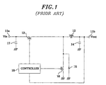
- a conventional step-down switching power supply including an inductor 12 (an inductor for performing a smoothing operation, referred to as an inductor hereinafter), a first switching device 13, a smoothing capacitor 14, a rectifying diode 15, a second switching device 16, a smoothing capacitor 17 and a control IC (integrated circuit), i.e., a controller 18.
- the first switching device 13 is, e.g., an P-channel field effect transistor (FET) and serves to convert an input voltage (V in ) provided from a battery (not shown) through an input terminal 11a to an output voltage (V out ) provided to an output terminal 11b via the inductor 12.
- FET field effect transistor
- the smoothing capacitor 14 is connected between the output terminal 11b and the ground.
- the rectifying diode 15 is connected in parallel with the series connection of the inductor 12 and the smoothing capacitor 14 to sustain an electric current of the inductor 12.
- the second switching device 16 is also an, e.g., N-channel FET and is coupled to the rectifying diode 15 in parallel.
- the smoothing capacitor 17 is coupled between the input terminal 11a and the ground.
- the controller 18 detects the output voltage (V out ) on the output terminal 11b and controls an on-off operation of the first and the second switching device 13 and 16 such that the output voltage (V out ) can be maintained at a predetermined level.
- the switching devices 13 and 16 are controlled in such a manner that when the first switching device 13 is on, the second switching device 16 is controlled to be turned off, and vice versa.
- the controller 18 adjusts pulse widths of pulse signals, which control the on-off conversions of the first and the second switching device 13 and 16, depending on a variation of the output voltage at the output terminal 11b to perform a feedback control. Accordingly, the regulated constant output voltage can be generated on the output terminal 11b.
- the controller 18 sets up a certain amount of dead time (t DET ) between an on-state of the first switching device 13 and that of the second switching device 16. Such dead time is required to prevent an undesirable cross current which can occur when both of the switching devices 13 and 16 are turned on concurrently.
- the energy accumulated in the inductor 12 can be emitted during a time period when the switching device 13 is off through the second switching device 16, even when connected to the output terminal 11b is a heavy load (not shown) requiring a great amount of electric current. Accordingly, a highly efficient synchronous rectification can be achieved without suffering from a forward voltage loss which can be otherwise caused by the rectifying diode 15.
- the respective switching devices 13 and 16 are respectively set to be on and off simultaneously when the input voltage from the battery is reduced down close to the output voltage; and the switching device 13 is maintained at a conduction state without performing any further switching operations in order to maintain the output voltage at the regulated level and extend the operating time of the battery operated power circuit.
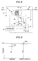
- the input voltage V in from the battery gradually decreases as the operation time of an electronic equipment increases.
- the output voltage V out declines slowly after the input voltage V in reaches a certain voltage value V 1 at a time t 1 .
- the output voltage V out continuously decreases to reach V min at a time t1' the input voltage V in decreases.
- the portable electronic equipment ceases its operation when V out drops down to V min , the minimum operation voltage of the electronic equipment.
- the operation time of the electronic device can be extended by t 1 ' - t 1 , which is limited by the considerably large constant voltage drop V drp .
- an object of the present invention to provide a battery-operated step-down power circuit having longer operating time with wide range of operating condition, a method for driving such power circuit, and an electronic component or module capable of implementing the power circuit.
- a power circuit capable of converting an input voltage into an output voltage through a switching and a smoothing operation, comprising: a switching device for performing the switching operation; an inductor for performing the smoothing operation, wherein the inductor is connected in series to the switching device; and a current control device connected in parallel to the switching device and/or the inductor.
- a power circuit having a switching device and an inductor connected in series between an input terminal and an output terminal, for generating an output voltage on the output terminal by lowering an input voltage provided through the input terminal by a switching operation of the switching device and monitoring the output voltage to maintain the output voltage at a substantially constant level
- the power circuit comprising: a current control device for adjusting an amount of an electric current provided from the input terminal to the output terminal in response to a control signal, wherein the current control device is connected between the input terminal and the output terminal in parallel to the switching device and an inductor; and a driving means for generating the control signal for controlling the current control device to maintain the output voltage at the constant level.
- a driving method of a power circuit having a switching device and an inductor connected in series between an input terminal and an output terminal, wherein the power circuit generates an output voltage on the output terminal by lowering an input voltage provided through the input terminal by a switching operation of the switching device and monitors the output voltage to maintain the output voltage at a substantially constant level
- the driving method comprising the steps of: providing a current control device for adjusting an amount of an electric current provided from the input terminal to the output terminal in response to a control signal, wherein the current control device is connected between the input terminal and the output terminal in parallel to the switching device and an inductor; and controlling a driving means for generating the control signal for controlling the current control device to maintain the output voltage at the constant level.
- an electronic component for use in a power circuit comprising: a package; an input terminal provided on the package; a first output terminal provided on the package; and a second output terminal provided on the package, wherein the package includes a switching device installed within the package and connected between the input terminal and the first output terminal; a current control device for changing an amount of an electric current provided from the input terminal to the second output terminal based on a control signal, wherein the current control device is installed within the package and connected between the input terminal and the second output terminal; a first control terminal connected to a control terminal of the switching device and installed to be exposed from the package; and a driving circuit for operating the current control device after the switching device is set to sustain an on duty factor of 100 %, wherein the driving circuit is installed within the package and connected to a control terminal of the current control device.
- a current control device e.g., a P-channel FET (field effect transistor) 21 and a driving circuit 22 thereof are added to the conventional power circuit described with reference to Fig. 1.
- a source and a drain of the FET 21 are connected to an input terminal 11a and an output terminal 11b, respectively, in parallel with the series connection of a first switching device 13 and an inductor 12.
- a gate of the FET 21 is connected to the driving circuit 22.
- the P-channel FET is connected in parallel with only one of the first switching device 13 and the inductor 12.
- the driving circuit 22 includes an N-channel FET 221, a resistor 222, a capacitor 223 and a diode 224.
- a source and a drain of the FET 221 are respectively coupled to the ground and the gate of the FET 21.
- a gate of the FET 221 is connected to a first terminal of the resistor 222 and an anode of the diode 224, and is also connected to the ground through the capacitor 223.
- a second terminal of the resistor 222 and a cathode of the diode 224 are coupled to the drain of the switching device 13.
- the first switching device 13 is switching operated by a controller 18 so that an output voltage V out is controlled to have a constant predetermined voltage value V set until an input voltage V in reaches a certain voltage value V 1 , as can be seen in Fig. 5.
- the FET 21 is set to be off until the input voltage V in drops to the voltage V 1 , and, thereafter, the FET 21 is set to be completely turned on to obtain a minimum turn-on resistance.
- a second switching device 16 is set to be off. During that period when the switching devices 13 and 16 are on and off, the capacitor 223 is charged through the resistor 222 and a gate voltage V G of the FET 221 gradually increases. Subsequently, when the switching device 16 is turned on, electric charges accumulated in the capacitor 223 are discharged through the diode 224 and the second switching device 16, and, therefore, the gate voltage V G of the FET 221 falls down to 0 V.
- the resistor 222 and the capacitor 223 are adapted to have such an RC time constant.
- a charging time constant of the capacitor 223 controls the gate voltage V G of the FET 221 so that the FET 221 does not turn to the on state while the switching device 16 is off.
- the FET 21 is also kept to be off during the time while the FET 221 is off.
- the FET 221 and the FET 21 remain to be off during the switching mode control period up to t 1.
- the first and the second switching device 13 and 16 are controlled by the controller 18 to be of the duty ratios or factors of 100% (always on) and 0% (always off), respectively.
- the gate voltage of the FET 221 is pulled up beyond a threshold voltage V th and the FET 221 is set to be on.
- the gate of the FET 21 is grounded and thus the FET 21 is set to be on.
- the output voltage V out is set to be V in - V drp1 and gradually declines as the input voltage V in from the battery decreases with time.
- V drp1 represents a voltage drop caused by a resultant resistance of the first switching device 13, the inductor 12 and the FET 21.
- V drp1 is smaller than the voltage drop V drp caused by the switching device 13 and the inductor 12 only as in the conventional power circuit shown in Fig. 1.
- the operation time of the equipment can be extended up to t 2 at which the output voltage V out reaches a minimum operation voltage V min of the equipment.
- the extended operation time t 2 - t 1 is greater than t 1 ' - t 1 of the conventional power circuit shown in Fig. 1 due to the reduced voltage drop V drp1 .
- FIG. 6 there is illustrated a block diagram of a power circuit in accordance with a second embodiment of the present invention.
- Fig. 7 is a timing chart for describing a switching operation thereof.
- the power circuit in accordance with the second embodiment differs from the power circuit of the first embodiment in that a P-channel FET 21 is controlled by a series driving control circuit 23.
- a source, a drain and a gate of the FET 21 are coupled to an input terminal 11a, an output terminal 11b and the series driving control circuit 23, respectively.
- the series driving control circuit 23 detects an output voltage V out and a gate voltage of a first switching device 13 and activates the FET 21 when the first switching device 13 becomes to have 100 % of on duty ratio(always on).
- the driving circuit 22 of Fig. 4 can be used to control a series driving controller 23'.
- the driving control circuit 23' is functionally identical to that of the series driving control circuit 23 in Fig. 6 excepting that the fact that the control circuit 23' converts an on-off state of the FET 21 depending on an output signal of the driving circuit 22 in lieu of that of a controller 18.
- the series driving control circuit 23 performs the so-called series operation as in a three terminal regulator to control the FET 21.
- the series driving control circuit 23 controls the turn-on resistance (a saturation voltage) of the FET 21 by varying the gate voltage of the FET 21 in order to provide the output voltage V out set to be a preset voltage V set .
- the amount of electric current provided through the FET 21 to the output terminal 11b is controlled, so that the output voltage V out is maintained at the preset level V set .
- the turn-on resistance of the FET 21 becomes minimum by the series driving control circuit 23 and the FET 21 becomes completely turned on.
- the operation time can be extended until the output voltage V out reaches the minimum voltage V min at a time t 4.
- the extended operation time t 4 - t 1 is much greater than that of t 1 '-t 1 of the prior art shown in Fig. 3.
- V out ⁇ V max there is required no such limitation of V out ⁇ V max as in the first preferred embodiment since the output voltage V out is maintained at a predetermined level, i.e., V set , by making the FET 21 perform the series operations after the on duty ratio of the first switching device 13 becomes 100 % at t 1 . Initiation of the series operation of the FET 21 after the on duty ratio of the first switching device 13 becomes 100 % is advantageous in terms of efficiency compared to the case where the series operation is initiated before the on duty ratio of the first switching device 13 reaches 100 %.
- the maximum output voltage of the power circuit can be increased.
- the output voltage is set to have the constant value V set after t 1 as shown in Fig. 7, the operation range of the power circuit can be enlarged for the input voltage.
- asynchronous rectification mode switching power circuit can be employed in lieu of the synchronous rectification mode switching power circuits in accordance with the preferred embodiments of the invention.
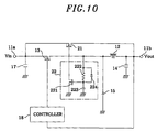
- Fig. 10 there is illustrated an exemplary asynchronous rectification mode power circuit obtained by removing the second switching device 16 from Fig. 4.
- Fig. 11 sets forth a perspective view of an electronic module or component 30 in accordance with a third preferred embodiment of the present invention and Fig. 12 is a circuit diagram thereof.
- the electronic component 30 is of a five-terminal SIP (Single In-line Package) type comprising a package 31, five lead terminals 32a to 32e and a heat radiation plate 33.
- SIP Single In-line Package
- the package 31 includes a driving circuit 22 as well as two FETs 41 and 42.
- the FETs 41 and 42 respectively correspond to the switching device 13 and the FET 21 in the first embodiment shown in Fig. 4 and the driving circuit 22 is identical to that of the first embodiment.
- Sources of the two FETs 41 and 42 are coupled to the lead terminal 32a and drains thereof are connected to the lead terminals 32b and 32c, respectively. Further, a gate of the FET 41 is led to the lead terminal 32d and that of the FET 42 is connected to a drain of an FET 221 of the driving circuit 22 as shown in Fig. 4.
- the driving circuit 22 is connected to the lead terminal 32b to receive an output signal from the FET 41.
- a ground terminal of the driving circuit 22 is connected to the lead terminal 32e.
- the power circuit in accordance with the first preferred embodiment shown in Fig. 4 can be implemented by using the electronic component 30 as shown in Figs 11 and 12.
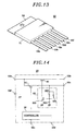
- Fig. 13 depicts a perspective view of an electronic component 50 in accordance with a fourth embodiment of the present invention and Fig. 14 offers a power circuit thereof.
- the electronic component 50 is of a shape of six-terminal SIP type including a package 51, six lead terminals 52a to 52f and a heat radiation plate 53.
- the package 51 has two FETs 41 and 42, a controller 18 and a driving circuit 22, wherein the two FETs 41 and 42 respectively correspond to the switching device 13 and the FET 21 of the first embodiment shown in Fig. 4 and a controller 18 and a driving circuit 22 are identical with those described therein.
- Sources of the FETs 41 and 42 are connected to the lead terminal 52a and drains of the FETs 41 and 42 are led to the lead terminal 52c and 52b, respectively.
- Gates of the FETs 41 and 42 are coupled to the controller 18 and the driving circuit 22, respectively.
- a feedback input of an output voltage V out and a control signal output of the controller 18 are connected to the lead terminals 52d and 52e. Further, there is installed a ground terminal 52f.
- the power circuit of the first preferred embodiment can be implemented by using the electronic component 50.
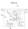
- FIG. 15 there is illustrated another exemplary electronic component 60 formed by adding a second switching device 16 and a rectification diode 15, both of which are presented in the first embodiment, to the package of the fourth embodiment of the present invention.
- FIG. 16 there is illustrated still another exemplary electronic component 70 having a series driving controller 23, as used in the second embodiment instead of the driving circuit 22.
- Bipolar transistors can be employed in lieu of the FETs. In this case, the control is accomplished by controlling a base current to alter a saturation current or a saturation voltage.
- a variable resistance device can be also employed as the current control device.
Landscapes
- Engineering & Computer Science (AREA)
- Power Engineering (AREA)
- Dc-Dc Converters (AREA)
- Control Of Electrical Variables (AREA)
Applications Claiming Priority (2)
| Application Number | Priority Date | Filing Date | Title |
|---|---|---|---|
| JP2000115045 | 2000-04-17 | ||
| JP2000115045A JP2001298945A (ja) | 2000-04-17 | 2000-04-17 | 電源回路の駆動方法並びに電源回路及び電源用電子部品 |
Publications (2)
| Publication Number | Publication Date |
|---|---|
| EP1148614A2 true EP1148614A2 (fr) | 2001-10-24 |
| EP1148614A3 EP1148614A3 (fr) | 2004-07-28 |
Family
ID=18626757
Family Applications (1)
| Application Number | Title | Priority Date | Filing Date |
|---|---|---|---|
| EP01109542A Withdrawn EP1148614A3 (fr) | 2000-04-17 | 2001-04-17 | Circuit de puissance alimenté par batterie et méthode de commande de cêlui-ci |
Country Status (6)
| Country | Link |
|---|---|
| US (1) | US6472854B2 (fr) |
| EP (1) | EP1148614A3 (fr) |
| JP (1) | JP2001298945A (fr) |
| KR (1) | KR20010098640A (fr) |
| HK (1) | HK1041566A1 (fr) |
| TW (1) | TW512576B (fr) |
Cited By (4)
| Publication number | Priority date | Publication date | Assignee | Title |
|---|---|---|---|---|
| WO2009118535A3 (fr) * | 2008-03-28 | 2009-11-26 | Deepstream Technologies Ltd | Régulateur linéaire avec coordination de passage par zéro |
| WO2011110933A3 (fr) * | 2010-03-11 | 2012-01-05 | Toyota Jidosha Kabushiki Kaisha | Circuit d'alimentation électrique à découpage et son procédé de commande |
| EP2637282A1 (fr) * | 2012-03-08 | 2013-09-11 | Hong Fu Jin Precision Industry (ShenZhen) Co. Ltd. | Circuit de décharge |
| CN110402534A (zh) * | 2017-03-31 | 2019-11-01 | 株式会社自动网络技术研究所 | 车辆用电源装置 |
Families Citing this family (21)
| Publication number | Priority date | Publication date | Assignee | Title |
|---|---|---|---|---|
| DE60030704T2 (de) * | 2000-07-10 | 2007-10-04 | Stmicroelectronics S.R.L., Agrate Brianza | Spannungschaltregler, mit einer Treiberschaltung eines MOS-Leistungsschalters |
| US6685334B2 (en) | 2002-04-30 | 2004-02-03 | G-5 Electronics | System and method of power management for a solar powered device |
| JP3835363B2 (ja) * | 2002-07-09 | 2006-10-18 | 株式会社デンソー | 車両用発電制御装置 |
| JP4017960B2 (ja) * | 2002-10-24 | 2007-12-05 | 日本テキサス・インスツルメンツ株式会社 | 駆動回路 |
| US6693410B1 (en) * | 2002-12-16 | 2004-02-17 | Adc Dsl Systems, Inc. | Power sequencing and ramp rate control circuit |
| DE10346325A1 (de) * | 2003-10-06 | 2005-05-04 | Siemens Ag | Schaltvorrichtung zum bidirektionalen Ladungsausgleich zwischen Energiespeichern |
| DE102004060359A1 (de) * | 2004-12-15 | 2006-07-06 | Austriamicrosystems Ag | Laderegleranordnung und Verfahren zum Aufladen einer Batterie |
| JP2007035068A (ja) * | 2006-10-16 | 2007-02-08 | Ricoh Co Ltd | 電源供給回路及び定電圧回路 |
| US7804287B2 (en) * | 2007-02-28 | 2010-09-28 | Rockwell Automation Technologies, Inc. | Low heat dissipation I/O module using direct drive buck converter |
| FI20070672A0 (fi) * | 2007-09-04 | 2007-09-04 | Efore Oyj | Menetelmä vaihtosähkön muodostamiseksi |
| JP5305334B2 (ja) * | 2008-09-02 | 2013-10-02 | 新電元工業株式会社 | ドライバ集積回路、ハーフブリッジ回路の駆動装置及び放電灯点灯装置 |
| JP2010136510A (ja) | 2008-12-03 | 2010-06-17 | Panasonic Corp | 降圧型スイッチングレギュレータ |
| JP2010200390A (ja) * | 2009-02-23 | 2010-09-09 | Toyota Motor Corp | 同期整流型dc−dcコンバータ |
| CN102130588B (zh) * | 2010-01-14 | 2013-09-18 | 全汉企业股份有限公司 | 电源供应装置 |
| US8248044B2 (en) * | 2010-03-24 | 2012-08-21 | R2 Semiconductor, Inc. | Voltage regulator bypass resistance control |
| US8917067B2 (en) | 2010-03-24 | 2014-12-23 | R2 Semiconductor, Inc. | Assisting an output current of a voltage converter |
| JP5970936B2 (ja) * | 2012-04-24 | 2016-08-17 | 株式会社ソシオネクスト | 電源回路 |
| US8994347B2 (en) * | 2012-06-04 | 2015-03-31 | R2 Semiconductor, Inc. | Assisting a load current of a switching voltage regulator |
| JP5603379B2 (ja) * | 2012-07-24 | 2014-10-08 | 株式会社ソニー・コンピュータエンタテインメント | 電気機器 |
| US9935470B2 (en) | 2015-10-27 | 2018-04-03 | Integrated Device Technology, Inc. | System and method for wireless power transfer using a power converter with a bypass mode |
| JP6274289B1 (ja) * | 2016-10-18 | 2018-02-07 | オムロン株式会社 | 電源回路 |
Family Cites Families (10)
| Publication number | Priority date | Publication date | Assignee | Title |
|---|---|---|---|---|
| US5148358A (en) * | 1991-04-03 | 1992-09-15 | Hughes Aircraft Company | Rectifier commutation current spike suppressor |
| US5422562A (en) * | 1994-01-19 | 1995-06-06 | Unitrode Corporation | Switching regulator with improved Dynamic response |
| CA2114507A1 (fr) * | 1994-01-28 | 1995-07-29 | Seshadri Sivakumar | Alimentation ininterruptible bimode a transfert rapide |
| US5552695A (en) * | 1994-03-22 | 1996-09-03 | Linear Technology Corporation | Synchronously rectified buck-flyback DC to DC power converter |
| US5877611A (en) * | 1996-10-09 | 1999-03-02 | Lucent Technologies Inc. | Simple and efficient switching regulator for fast transient loads such as microprocessors |
| FR2754955B1 (fr) * | 1996-10-22 | 1998-12-24 | Sgs Thomson Microelectronics | Dispositif de limitation de variations transitoires d'une tension d'alimentation |
| US6043705A (en) * | 1998-03-25 | 2000-03-28 | Lucent Technologies Inc. | Boost converter having extended holdup time and method of operation |
| US5998977A (en) * | 1998-05-27 | 1999-12-07 | Maxim Integrated Products, Inc. | Switching power supplies with linear precharge, pseudo-buck and pseudo-boost modes |
| US6259235B1 (en) * | 1999-08-26 | 2001-07-10 | Tyco Electronics Logistics Ag | Active clamp for power converter and method of operation thereof |
| US6232755B1 (en) * | 2000-01-31 | 2001-05-15 | Intel Corporation | Switching voltage regulator that adjusts a timing in response to a load transient |
-
2000
- 2000-04-17 JP JP2000115045A patent/JP2001298945A/ja not_active Withdrawn
-
2001
- 2001-03-29 TW TW090107530A patent/TW512576B/zh not_active IP Right Cessation
- 2001-04-16 KR KR1020010020260A patent/KR20010098640A/ko not_active Ceased
- 2001-04-17 EP EP01109542A patent/EP1148614A3/fr not_active Withdrawn
- 2001-04-17 US US09/836,162 patent/US6472854B2/en not_active Expired - Fee Related
-
2002
- 2002-04-24 HK HK02103059.0A patent/HK1041566A1/en unknown
Cited By (6)
| Publication number | Priority date | Publication date | Assignee | Title |
|---|---|---|---|---|
| WO2009118535A3 (fr) * | 2008-03-28 | 2009-11-26 | Deepstream Technologies Ltd | Régulateur linéaire avec coordination de passage par zéro |
| WO2011110933A3 (fr) * | 2010-03-11 | 2012-01-05 | Toyota Jidosha Kabushiki Kaisha | Circuit d'alimentation électrique à découpage et son procédé de commande |
| US9276466B2 (en) | 2010-03-11 | 2016-03-01 | Toyota Jidosha Kabushiki Kaisha | Switching power supply circuit and control method therefor |
| EP2637282A1 (fr) * | 2012-03-08 | 2013-09-11 | Hong Fu Jin Precision Industry (ShenZhen) Co. Ltd. | Circuit de décharge |
| CN110402534A (zh) * | 2017-03-31 | 2019-11-01 | 株式会社自动网络技术研究所 | 车辆用电源装置 |
| CN110402534B (zh) * | 2017-03-31 | 2021-02-26 | 株式会社自动网络技术研究所 | 车辆用电源装置 |
Also Published As
| Publication number | Publication date |
|---|---|
| KR20010098640A (ko) | 2001-11-08 |
| JP2001298945A (ja) | 2001-10-26 |
| US20010030528A1 (en) | 2001-10-18 |
| HK1041566A1 (en) | 2002-07-12 |
| US6472854B2 (en) | 2002-10-29 |
| TW512576B (en) | 2002-12-01 |
| EP1148614A3 (fr) | 2004-07-28 |
Similar Documents
| Publication | Publication Date | Title |
|---|---|---|
| EP1148614A2 (fr) | Circuit de puissance alimenté par batterie et méthode de commande de cêlui-ci | |
| US8120338B2 (en) | Dropper-type regulator | |
| US7548050B2 (en) | Switching power supply device and semiconductor integrated circuit | |
| CN100379135C (zh) | 电源电路 | |
| US7262587B2 (en) | Circuit and method for controlling DC-DC converter | |
| US7098639B2 (en) | DC-DC converter and method for controlling DC-DC converter | |
| JP4471978B2 (ja) | スイッチング電源制御回路およびスイッチング電源装置ならびにそれを用いた電子機器 | |
| JP4728718B2 (ja) | 昇圧型スイッチングレギュレータおよびその制御回路ならびにそれを用いた電子機器 | |
| US9350236B2 (en) | Switching regulator with reduced body diode conduction | |
| US6294903B1 (en) | Switching power supply | |
| JPH09140126A (ja) | 適応スイッチ回路、適応出力回路、制御回路およびスイッチング電圧レギュレータを動作させる方法 | |
| JP2008177019A (ja) | Led駆動回路 | |
| EP1696565B1 (fr) | Circuit inverseur utilisant un circuit de tampon de grille | |
| US20080290734A1 (en) | Switching pulse generating circuit and regulator using the same | |
| US7911192B2 (en) | High voltage power regulation using two power switches with low voltage transistors | |
| US20210006244A1 (en) | Drive circuit | |
| TW202046823A (zh) | 積體電路設備及其操作方法 | |
| JP2005261009A (ja) | スイッチング電源回路及びそれを用いた電子機器 | |
| JP2002051541A (ja) | スイッチング電源装置及びスイッチング電源用半導体装置 | |
| JPH08205528A (ja) | 昇降圧型スイッチング電源 | |
| KR100641259B1 (ko) | 승압형 스위칭 레귤레이터 회로 | |
| JP2005295630A (ja) | 電源装置及び電源制御回路 | |
| JP4609285B2 (ja) | 電源用半導体集積回路および電源装置 | |
| JP2011015606A (ja) | 電子機器 |
Legal Events
| Date | Code | Title | Description |
|---|---|---|---|
| PUAI | Public reference made under article 153(3) epc to a published international application that has entered the european phase |
Free format text: ORIGINAL CODE: 0009012 |
|
| AK | Designated contracting states |
Kind code of ref document: A2 Designated state(s): AT BE CH CY DE DK ES FI FR GB GR IE IT LI LU MC NL PT SE TR |
|
| AX | Request for extension of the european patent |
Free format text: AL;LT;LV;MK;RO;SI |
|
| PUAL | Search report despatched |
Free format text: ORIGINAL CODE: 0009013 |
|
| AK | Designated contracting states |
Kind code of ref document: A3 Designated state(s): AT BE CH CY DE DK ES FI FR GB GR IE IT LI LU MC NL PT SE TR |
|
| AX | Request for extension of the european patent |
Extension state: AL LT LV MK RO SI |
|
| AKX | Designation fees paid | ||
| REG | Reference to a national code |
Ref country code: DE Ref legal event code: 8566 |
|
| STAA | Information on the status of an ep patent application or granted ep patent |
Free format text: STATUS: THE APPLICATION IS DEEMED TO BE WITHDRAWN |
|
| 18D | Application deemed to be withdrawn |
Effective date: 20050129 |
|
| REG | Reference to a national code |
Ref country code: HK Ref legal event code: WD Ref document number: 1041566 Country of ref document: HK |