EP1148633A1 - Circuit à haute fréquence utilisant un bloc de cellules amplificateur à sortie de puissance haute et un bloc de cellules amplificateur à sortie de puissance basse - Google Patents
Circuit à haute fréquence utilisant un bloc de cellules amplificateur à sortie de puissance haute et un bloc de cellules amplificateur à sortie de puissance basse Download PDFInfo
- Publication number
- EP1148633A1 EP1148633A1 EP01303251A EP01303251A EP1148633A1 EP 1148633 A1 EP1148633 A1 EP 1148633A1 EP 01303251 A EP01303251 A EP 01303251A EP 01303251 A EP01303251 A EP 01303251A EP 1148633 A1 EP1148633 A1 EP 1148633A1
- Authority
- EP
- European Patent Office
- Prior art keywords
- cell block
- amplifier cell
- output amplifier
- output
- amplifier
- Prior art date
- Legal status (The legal status is an assumption and is not a legal conclusion. Google has not performed a legal analysis and makes no representation as to the accuracy of the status listed.)
- Granted
Links
Images






Classifications
-
- H—ELECTRICITY
- H01—ELECTRIC ELEMENTS
- H01P—WAVEGUIDES; RESONATORS, LINES, OR OTHER DEVICES OF THE WAVEGUIDE TYPE
- H01P5/00—Coupling devices of the waveguide type
- H01P5/08—Coupling devices of the waveguide type for linking dissimilar lines or devices
- H01P5/10—Coupling devices of the waveguide type for linking dissimilar lines or devices for coupling balanced lines or devices with unbalanced lines or devices
- H01P5/107—Hollow-waveguide/strip-line transitions
-
- H—ELECTRICITY
- H03—ELECTRONIC CIRCUITRY
- H03F—AMPLIFIERS
- H03F1/00—Details of amplifiers with only discharge tubes, only semiconductor devices or only unspecified devices as amplifying elements
- H03F1/02—Modifications of amplifiers to raise the efficiency, e.g. gliding Class A stages, use of an auxiliary oscillation
- H03F1/0205—Modifications of amplifiers to raise the efficiency, e.g. gliding Class A stages, use of an auxiliary oscillation in transistor amplifiers
- H03F1/0283—Reducing the number of DC-current paths
-
- H—ELECTRICITY
- H03—ELECTRONIC CIRCUITRY
- H03F—AMPLIFIERS
- H03F3/00—Amplifiers with only discharge tubes or only semiconductor devices as amplifying elements
- H03F3/72—Gated amplifiers, i.e. amplifiers which are rendered operative or inoperative by means of a control signal
-
- H—ELECTRICITY
- H03—ELECTRONIC CIRCUITRY
- H03F—AMPLIFIERS
- H03F2203/00—Indexing scheme relating to amplifiers with only discharge tubes or only semiconductor devices as amplifying elements covered by H03F3/00
- H03F2203/72—Indexing scheme relating to gated amplifiers, i.e. amplifiers which are rendered operative or inoperative by means of a control signal
- H03F2203/7236—Indexing scheme relating to gated amplifiers, i.e. amplifiers which are rendered operative or inoperative by means of a control signal the gated amplifier being switched on or off by putting into parallel or not, by choosing between amplifiers by (a ) switch(es)
-
- H—ELECTRICITY
- H10—SEMICONDUCTOR DEVICES; ELECTRIC SOLID-STATE DEVICES NOT OTHERWISE PROVIDED FOR
- H10W—GENERIC PACKAGES, INTERCONNECTIONS, CONNECTORS OR OTHER CONSTRUCTIONAL DETAILS OF DEVICES COVERED BY CLASS H10
- H10W44/00—Electrical arrangements for controlling or matching impedance
- H10W44/20—Electrical arrangements for controlling or matching impedance at high-frequency [HF] or radio frequency [RF]
- H10W44/226—Electrical arrangements for controlling or matching impedance at high-frequency [HF] or radio frequency [RF] for HF amplifiers
-
- H—ELECTRICITY
- H10—SEMICONDUCTOR DEVICES; ELECTRIC SOLID-STATE DEVICES NOT OTHERWISE PROVIDED FOR
- H10W—GENERIC PACKAGES, INTERCONNECTIONS, CONNECTORS OR OTHER CONSTRUCTIONAL DETAILS OF DEVICES COVERED BY CLASS H10
- H10W72/00—Interconnections or connectors in packages
- H10W72/50—Bond wires
- H10W72/541—Dispositions of bond wires
- H10W72/5445—Dispositions of bond wires being orthogonal to a side surface of the chip, e.g. parallel arrangements
-
- H—ELECTRICITY
- H10—SEMICONDUCTOR DEVICES; ELECTRIC SOLID-STATE DEVICES NOT OTHERWISE PROVIDED FOR
- H10W—GENERIC PACKAGES, INTERCONNECTIONS, CONNECTORS OR OTHER CONSTRUCTIONAL DETAILS OF DEVICES COVERED BY CLASS H10
- H10W72/00—Interconnections or connectors in packages
- H10W72/50—Bond wires
- H10W72/541—Dispositions of bond wires
- H10W72/547—Dispositions of multiple bond wires
- H10W72/5475—Dispositions of multiple bond wires multiple bond wires connected to common bond pads at both ends of the wires
Definitions
- the present invention relates to a high frequency circuit for realizing a high efficiency power amplifier with a wide output power range which is suitable for use in a portable telephone or the like, for example, and a communication device using such a high frequency circuit.
- the power amplifier has an efficiency which lowers at low'output, because its power addition efficiency increases as the output power is increased and takes the maximum value in a vicinity of the saturation point of the output power.
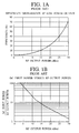
- Fig. 1A shows an exemplary relationship between the efficiency and the output power at low output in a general amplifier.
- the efficiency is a value obtained by dividing an RF (high output) output power by a DC (direct current) input power, which corresponds to a collector efficiency of a bipolar transistor and a drain efficiency of a field effect transistor.
- Fig. 1B shows an inverse of the efficiency shown in Fig. 1A in the logarithmic scale.
- the efficiency is sequentially degraded from 72% at the output power of 30 dBm (dBmW to be accurate, but will be abbreviated as dBm hereafter) to 21.8% at the output power of 20 dBm, 4.7% at the output of 10 dBm, and 1,5% at the output power of 5 dBm. Accordingly, a ratio of the DC input power with respect to the RF output power sequentially increases to 1.4 at the 30 dBm output, 4.6 at the 20 dBm output, 21.2 at the 10 dBm output, and 67.1 at the 5 dBm output.
- FIGs. 2A and 2B show graphs indicating a relationship between current and voltage in the alternating currents.
- a load line is as indicated by a chain line KB
- the output voltage is in a form of a sinusoidal wave with an average value set at a bias voltage
- the output current is in a form of a half-wave rectified wave Iout(t). Note that a point B in Figs. 2A and 2B corresponds to the bias point.
- Figs. 2A and 2B show the case of the class B operation.
- the RF output power is given by a product of an effective value of the fundamental wave component Vout of the output power and an effective value of the fundamental wave component I 1 (t).
- Vout of the output power an effective value of the fundamental wave component
- I 1 (t) an effective value of the fundamental wave component
- the DC input power is given by a product of the bias and an average value of the output current Iout(t), which corresponds to an area of a rectangle with a point D and a point B as diagonal corners (which will be referred to as a rectangle DB hereafter) in Figs. 2A and 2B.
- the efficiency is given by a ratio of these two areas.
- the current amplitude and the voltage amplitude are both reduced to 1/2 so that the output power is 1/4.
- the direct current is given by an average value of the RF current so that it is also reduced to 1/2 but the direct current voltage is fixed at a point B, so that the area of the rectangle DB is 1/2.
- the efficiency is reduced to 1/2 whenever the RF output power is reduced to 1/4 (-6 dB).
- a rate of the degradation of the efficiency is greater than 1/2 due to the influence of the knee voltage or the fact that the operation is actually the class AB operation.
- a plurality of amplifiers with different maximum output powers AMP1 (with maximum output of -20 dBm) AMP2 (with maximum output of 5 dBm), and AMP3 (with maximum output of 30 dBm) are arranged in series, while bias circuits 75 and 76 are provided with respect to the AMP2 and AMP3 of the later stages, and a connection form is selected by switching switch circuits S71. S72, S73 and S74, so as to realize an appropriate power amplification.
- the gain of each stage is usually about 25 dB, so that it is difficult to improve the degradation of the efficiency considerably by the method described above.
- the minimum unit for the amplification stages that is practically feasible is expected to be 10 dB to 15 dB corresponding to the gain per one stage of a transistor.
- Fig. 4A shows a circuit for realizing this conventional optimization method schematically.
- a circuit shown in Fig. 4A realizes a method for switching an effective transistor size of the amplifier, where a plurality of amplifiers 14a and 14b are connected in parallel, while input switches Si1 and Si2 and output switches So1 and So2 are provided at the input side and the output side of these transistors 14a and 14b respectively, and input signals entered from a variable matching circuit 13i are entered into a transistor with appropriate gate length or emitter area by switching the switches Si1, Si2, So1 and So2 and amplified signals are outputted to a variable matching circuit 13o.
- the matching to a matching condition suitable for a respective transistor size is made by the variable matching circuits 13i and 13o.
- the maximum output power is reduced to 1/2 by reducing the transistor size to 1/2, so that the efficiency can be maximized for the power in a narrow range of about 3 dB.
- Such a variable matching circuit can be realized by any of a circuit shown in Fig. 5A in which a variable inductance 11 and a variable capacitor 12 are combined, a circuit shown in Fig. 5B in which distributed constant circuits 14 to 16 are connected through switches S1 and S2, and a circuit shown in Fig. 5C in which matching circuits 13a and 13b of different types are switched by switches Si11, Si12, So11 and So12.
- a circuit shown in Fig. 5C in which matching circuits 13a and 13b of different types are switched by switches Si11, Si12, So11 and So12.
- FIG. 6A Another way of compensating the degradation of the efficiency at low output is to use an amplifier circuit as shown in Fig. 6A.
- This amplifier circuit realizes a method for optimizing the power source voltage to be supplied to the amplifier according to the output power, where a voltage Vdc to be applied to a transistor 17 is adjusted by variable voltage sources 9 and 10 so as to move the bias point from B2 to B1 and change the load line from K2B2 to K1B1 as shown in Fig. 6B, such that the power and the voltage amplitude on the load line are maximized.
- the matching of input/output can be made by constant matching circuits 18i and 18o rather than variable matching circuits.
- a variable voltage source with sufficiently high efficiency capable of supplying a large amount of currents to be consumed by the power amplifier can be realized by a step-down DC-DC converter as shown in Fig. 6C in which a resistance L and a capacitor C are appropriately connected by switches Q1 and Q2 controlled by a control circuit.
- the lowest output voltage is only about 1 V due to the reference voltage of the internal regulator, and the efficiency of the variable voltage source is degraded at the low voltage output, so that it is difficult to maintain the high efficiency over a wide output power range and there is also a problem that the implementation area is large.
- the transmission power control is carried out in the communication system using the CDMA scheme, such that the transmission power varies within a range (dynamic range) of about 75 dB. Consequently, the power addition efficiency of the power amplifier is required to be high at the powers other than the maximum output power.
- the probability density function for the transmission powers is roughly in a form of the normal distribution, and the average transmission power of the mobile terminal is in a range of 10 dBm to 16 dBm, although it varies due to system related factors such as the arrangement of the base stations.
- a high frequency circuit comprising: a high output amplifier cell block configured to amplify input signals at a time of high output power, in which a DC power source voltage is supplied in parallel to first amplifier cells that are connected in parallel AC-wise with respect to input/output signals; a low output amplifier cell block configured to amplify the input signals at a time of low output power, in which the DC power source voltage is supplied in series to second amplifier cells that are connected in parallel AC-wise with respect to the input/output signals; a first connection unit configured to connect input sides of the high output amplifier cell block and the low output amplifier cell block with an input terminal from which the input signals are entered; and a second connection unit configured to connect output sides of the high output amplifier cell block and the low output amplifier cell block with an output terminal to which output signals are outputted.
- a communication device comprising: at least one antenna configured to transmit or receive radio signals; at least one power amplifier configured to amplify the radio signals to be transmitted or received by the at least one antenna, including a high frequency circuit formed by: a high output amplifier cell block configured to amplify input signals at a time of high output power, in which a DC power source voltage is supplied in parallel to first amplifier cells that are connected in parallel AC-wise with respect to input/output signals; a low output amplifier cell block configured to amplify the input signals at a time of low output power, in which the DC power source voltage is supplied in series to second amplifier cells that are connected in parallel AC-wise with respect to the input/output signals; a first connection unit configured to connect input sides of the high output amplifier cell block and the low output amplifier cell block with an input terminal from which the input signals are entered; and a second connection unit configured to connect output sides of the high output amplifier cell block and the low output amplifier cell block with an output terminal to which output signals are outputted; and
- Figs. 1A and 1B are graphs showing a relationship between the RF output power and the efficiency in a conventional power amplifier.
- Figs. 2A and 2B are diagrams for explaining a lowering of the efficiency at low output in a conventional power amplifier.
- Figs. 3A and 3B are a connection diagram and a gain diagram for explaining one exemplary conventional amplifier circuit.
- Figs. 4A and 4B are a connection diagram and a graph showing a relationship between current and voltage for explaining another exemplary conventional amplifier circuit.
- Figs. 5A, 5B and 5C are diagrams showing exemplary circuits that can be used as a variable matching circuit in the conventional amplifier circuit of Fig. 4A.
- Figs. 6A and 6B are a connection diagram and a graph showing a relationship between current and voltage for explaining another exemplary conventional amplifier circuit.
- Fig. 6C is a diagram showing an exemplary circuit that can be used as a variable voltage source in the conventional amplifier circuit of Fig. 6A.
- Fig. 7 is a block diagram showing a configuration of a power amplifier using a high frequency circuit according to the first embodiment of the present invention.
- Fig. 8 is a block diagram showing an operation state of the power amplifier of Fig. 7.
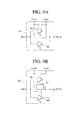
- Figs. 9A and 9B are diagrams respectively showing internal configurations of a high output amplifier cell block and a low output amplifier cell block in the power amplifier of Fig. 7.
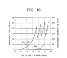
- Fig. 10 is a graph showing a relationship between the output power and the efficiency in the power amplifier of Fig. 7.
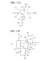
- Figs 11A and 11B are circuit diagrams respectively showing equivalent circuits of a high output amplifier cell block and a low output amplifier cell block in the power amplifier of Fig. 7.
- Fig. 12 is a block diagram showing a configuration of a power amplifier using a high frequency circuit according to the second embodiment of the present invention.
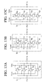
- Figs. 13A, 13B and 13C are diagrams respectively showing internal configurations of a high output amplifier cell block, a middle output amplifier cell block and a low output amplifier cell block in the power amplifier of Fig. 12.
- Fig. 14 is a block diagram showing a configuration of a power amplifier using a high frequency circuit according to the third embodiment of the present invention.
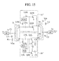
- Fig. 15 is a block diagram showing a configuration of a power amplifier using a high frequency circuit according to the fourth embodiment of the present invention.
- Figs. 16A and 16B are diagrams showing exemplary configurations of a power amplifier using a high frequency circuit according to the fifth embodiment of the present invention.
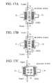
- Figs. 17A, 17B and 17C are diagrams showing exemplary configurations of a power amplifier using a high frequency circuit according to the fifth embodiment of the present invention.
- Figs. 18A and 18B are diagrams showing exemplary configurations of a power amplifier using a high frequency circuit according to the fifth embodiment of the present invention.
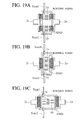
- Figs. 19A, 19B and 19C are diagrams showing exemplary configurations of a power amplifier using a high frequency circuit according to the sixth embodiment of the present invention.
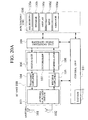
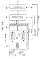
- Figs. 20A and 20B are diagrams showing exemplary configurations of communication devices using a high frequency circuit of the present invention according to the seventh embodiment of the present invention.
- a phrase "amplifier cells connected in parallel AC-wise" will be used to imply that target amplifier cells of nearly identical size are connected at nearly identical phase with nearly identical amplitude. Strictly speaking from a viewpoint of distributed constant circuits, a connection at exactly identical phase with exactly identical amplitude is difficult to realize in practice, so that a phase "amplifier cells connected in parallel AC-wise" can be construed as meaning that the efficiencies of the power distribution at the input side and the power composition at the output side of a plurality of cell blocks, such as cell blocks 4a and 4b, 4c and 4d shown in Figs. 9A and 9B to be described below or transistors Q1 and Q2 shown in Figs.
- a phrase “DC power source voltage is supplied in parallel” will be used to imply that nearly identical level of voltage is applied to target cells. Strictly speaking, it is practically difficult to apply exactly identical level of voltage because of a voltage dropping due to circuit losses, so that a phrase “DC power source voltage is supplied in parallel” can be construed as meaning that the voltage is applied within a tolerable range of ⁇ 20% with respect to a plurality of cell blocks, such as cell blocks 4a to 4c shown in Figs. 9A and 9B to be described below, or cells that constitute these cell blocks.
- a phrase "DC power source voltage is supplied in series” will be used to imply that, when the "amplifier cells connected in parallel AC-wise" are transistor cells Q1 and Q2 as shown in Fig. 11B to be described below, the voltage given at a collector of the transistor cell Q1 is applied to these plurality of transistor cells in division, in such a way that the DC flows from a collector of the transistor cell Q1 through an emitter to a collector of the transistor cell Q2 and is then grounded, for example.
- transistor cell will be used to indicate a set of transistors having nearly identical characteristics. Strictly speaking from a viewpoint of the device process, it is practically difficult to fabricate transistors with exactly identical characteristics. Even if geometrically similar transistors are used, they may not operate as identical transistors depending on their layout positions on a semiconductor chip or differences in their surrounding electromagnetic and thermal environments due to a substrate on which the semiconductor chip is implemented, etc. Also, even within a semiconductor wafer, geometrically similar transistors may not necessary have identical characteristics, due to the non-uniformity of characteristics which is a well known problem associated with transistors in general.
- a set of transistors are formed by bundling a plurality of tiny unit transistors (in units of gate in the case of FETs, in units of emitter or base in the case of bipolar transistors, for example) that are physically independent in the power amplifier. If a sufficient power cannot be obtained in this state, an even larger transistor is formed by bundling these transistors.
- a transistor used in the power amplifier is a set of a plurality of tiny transistors in general.
- Fig. 7 shows an exemplary configuration of a power amplifier formed by using a high frequency circuit of this embodiment.
- the power amplifier comprises an input matching circuit 3i, a first connection unit 2i for splitting signals entered from the input matching circuit 3i, a high output amplifier cell block 1a, a low output amplifier cell block 1b, a second connection unit 2o to which signals from the high output amplifier cell block 1a and the low output amplifier cell block 1b are entered, and an output matching circuit 3o.
- the high output amplifier cell block 1a has amplifier cells which are connected in parallel AC-wise with respect to input and output signals, and DC power source voltage is supplied in parallel to these amplifier cells.
- the low output amplifier cell block 1b has amplifier cells that are connected in parallel AC-wise with respect to input and output signals, and DC power source voltage is supplied in series to these amplifier cells.
- the high output amplifier cell block 1a has a signal input terminal INa, a signal output terminal OUTa, a power source voltage terminal Vdca, and a control voltage terminal Vcnta
- the low output amplifier cell block 1b has a signal input terminal INb, a signal output terminal OUTb, a power source voltage terminal Vdcb, and a control voltage terminal Vcntb.
- each one of the first and second connection units 2i and 2o is formed by using only passive elements such as coils and capacitors, so as to provide a splitting circuit formed by transmission paths, for example, as indicated in the second connection unit 2o shown in Fig. 8.
- the use of active elements for switching signal paths such as switches used in the conventional circuits of Figs. 4A, 5A, 5B and 5C in addition to active elements for amplifying RF signals can cause the complication of a circuit configuration, the increase of the required number of parts, the increase of the implementation area, and the degradation of signals due to distortion or loss, which can lead to the higher cost and the lower performance.
- the use of such active elements is avoided in this embodiment and the first and second connection units 2i and 2o are formed by using only passive elements in order to achieve the equivalent or better effects by a simpler configuration.
- Fig. 9A and Fig. 9B show exemplary internal configurations of the high output amplifier cell block 1a and the low output amplifier cell block 1b respectively. Note that amplifier cells 4a, 4b, 4c and 4d used in this embodiment are formed by transistors of the same size.
- the high output amplifier cell block 1a of this embodiment has two amplifier cells 4a and 4b, and these amplifier cells 4a and 4b are connected in parallel with respect to the input and output signals, and also connected in parallel with respect to the DC power source voltage Vdca.
- the control voltage Vcnta is also given in parallel to the amplifier cells 4a and 4b.
- the low output amplifier cell block 1b of this embodiment has two amplifier cells 4c and 4d, and these amplifier cells 4c and 4d are connected in parallel with respect to the input and output signals, and also connected in series with respect to the DC power source voltage Vdcb.
- the control voltage Vcntb is also given in parallel to the amplifier cells 4c and 4d.
- the amplifier cells 4c and 4d in the low output amplifier cell block 1b are connected by an AC/DC separation unit 5 such as bias T, for example, and this AC/DC separation unit 5 realizes a grounding of AC of the amplifier cell 4c, while DC is applied to the DC power source terminal of the amplifier cell 4d.
- the DC power source voltage applied to the amplifier cells 4c and 4d is divided into two equal parts, i.e., 1/2 each.
- the number of the amplifier cells 4a and 4b in the high output amplifier cell block 1a is set equal to the number of the amplifier cells 4c and 4d in the low output amplifier cell block 1b, so that the input and output impedances are equal ideally speaking. Consequently, the slopes of the load lines can be made identical by using the common input and output matching circuits 3i and 3o.
- the power source voltage is 1/2 and the load line is identical so that the maximum current also becomes 1/2 and the maximum output power can be reduced to 1/4 (-6 dB).
- This embodiment is equivalent to a state in which the bias voltage B1 becomes 1/2 of the bias voltage B2 in Fig. 6B.
- the maximum output power of the high output amplifier cell block 1a is set to 30 dBm
- the maximum output power of the low output amplifier cell block 1b can be about 24 dBm because the power source voltage is 1/2.
- the high output amplifier cell block 1a is put in an operation state while the low output amplifier cell block 1b is put in a non-operation state.
- the efficiency will be lowered as the output power becomes lower than the maximum output power 30 dBm.
- the output power is about 24 dBm which is the maximum output power of the low output amplifier cell block 1b
- the efficiency is lowered to 35.4%.
- the high output amplifier cell block 1a is put in a non-operation state while the low output amplifier block 1b is put in an operation state, such that the efficiency is recovered to 72% again, and them lowered to 35% again as the output power is lowered further.
- the efficiency can be recovered to about 72% even at the low output, so that a relationship between the efficiency and the output power becomes a saw-tooth shaped line with about 6 dB interval between adjacent peaks as shown in Fig. 10.
- Figs. 11A and 11B show equivalent circuits of the high output amplifier cell block 1a and the low output amplifier cell block 1b shown in Figs. 9A and 9B respectively.
- C1, C1' and C2 are DC preventing capacitors
- L1, L1' and L2 are RF chokes
- R1 and R1' are stabilizing resistors
- Q1 and Q2 are bipolar transistors. Note that the same effects can also be realized by using field effect transistors for Q1 and Q2.
- C3 is a DC preventing capacitor for separating collectors of Q1 and Q2 DC-wise
- C4 and L4 forms a filter which functions as the AC/DC separation unit 5 in this embodiment. Namely, C4 realizes the AC-wise grounding in the signal frequency of Q1.
- the power amplifier according to this embodiment in a configuration as described above operates as follows.
- signals entered from an input terminal IN are entered into the high output amplifier cell block 1a and the low output amplifier cell block 1b through the input matching circuit 3i and the first connection unit 2i.
- the output signals of the high output amplifier cell block 1a and the low output amplifier cell block 1b are outputted from an output terminal OUT through the second connection unit 2o and the output matching circuit 3o.
- one of the amplifier cell blocks 1a and 1b is selected according to the power to be outputted, and these amplifier cell blocks 1a and 1b are switched between an amplification operation state and a non-operation state with high impedance, by the control voltages Vcnta and Vcntb. Only one amplifier cell block is put in the amplification operation state at any given moment. For example, as shown in Fig. 8, when the high output amplifier cell block 1a is put in the amplification operation state, the low output amplifier cell block 1b is put in a high impedance non-operation state.
- the input and output impedances of the low output amplifier cell block 1b in the high impedance non-operation state can be expressed as capacitances Ci and Co respectively.
- the resistance component that is entered into open capacitances is ignored here as it only causes a negligible loss compared with the output impedance of the high output cell block 1a.
- the load impedance from a viewpoint of an output node 6a of the high output amplifier cell block 1a is that of a parallel connection of the output matching circuit 3o and a stab with the open capacitance Co beyond a splitting point node 6c.
- the operating amplifier cell block can be selected without using any switch.
- the first embodiment described above is directed to the case of using two amplifier cell blocks as shown in Fig. 7, but the present invention is not limited to this specific case.
- the number of steps connected in series with respect to DC in the low output amplifier cell block is two in the first embodiment, but this number can be increased to four, eight, and so on.
- four steps for example, the three types of amplifier cell blocks using one step, two steps, and four steps may be used, or two types of amplifier cell blocks using one step and four steps may be used.
- eight steps four types of amplifier cell blocks using one step, two steps, four steps and eight steps may be used, or any three types out of these four types may be used, or any two types out of these four types may be used. It should be apparent that the circuit configuration becomes more complicated when the number of steps is increased. The number of steps to be used should be selected by taking the effect at a time of the power control into consideration.
- the number of steps need not takes a form of 2 n , but it is assumed to be in a form of 2 n here.
- N 2 n
- up to n+1 types of the amplifier cell blocks using the respective number of steps equal to 1, 2, 4, ⁇ , 2 n can be used.
- the choice of the types of the amplifier cell blocks to be used in combination is arbitrary as described above, but it should be noted that the use of the same number of steps in different amplifier cell blocks would result in a poor circuit efficiency.
- the dynamic range greater than or equal to 12 dB can be realized.
- the power amplifier comprises an input matching circuit 3i, a first connection unit 2i for splitting signals entered from the input matching circuit 3i, a high output amplifier cell block 1c, a middle output amplifier cell block 1d, a low output amplifier cell block 1e, a second connection unit 2o to which signals from the high output amplifier cell block 1c, the middle output amplifier cell block 1d and the low output amplifier cell block 1e are entered, and an output matching circuit 3o.
- the high output amplifier cell block 1c of this embodiment has four amplifier cells 4e to 4h, and these amplifier cells 4e to 4h are connected in parallel with respect to the input and output signals, and also connected in parallel with respect to the DC power source voltage Vdcc.
- the control voltage Vcntc is also given in parallel to the amplifier cells 4e to 4h.
- the middle output amplifier cell block 1d of this embodiment has two amplifier cells 4i and 41, and these amplifier cells 4i to 41 are connected in parallel with respect to the input and output signals. Also, a pair of the amplifier cells 4i and 4j and a pair of the amplifier cells 4k and 41 are connected in series with respect to the DC power source voltage Vdcd while the first stage amplifier cells 4i and 4k of these pairs are connected in parallel. In addition, the control voltage Vcntd is also given in parallel to the amplifier cells 4i and 41.
- Each pair of the amplifier cells 4i and 4j, or 4k and 41, in the middle output amplifier cell block 1d are connected by an AC/DC separation unit 5 such as bias T, for example, and this AC/DC separation unit 5 realizes a grounding of AC of the amplifier cells 4i and 4k, while DC is applied to the DC power source terminals of the second stage amplifier cells 4j and 41.
- the DC power source voltage applied to the amplifier cells 4i to 41 is divided into two equal parts, i.e., 1/2 each.
- the low output amplifier cell block 1e of this embodiment has four amplifier cells 4m to 4p, and these amplifier cells 4m to 4p are connected in parallel with respect to the input and output signals, and also connected in series with respect to the DC power source voltage Vdce.
- the control voltage Vcnte is also given in parallel to the amplifier cells 4m to 4p.
- the amplifier cells 4m to 4p in the low output amplifier cell block 1e are connected by an AC/DC separation unit 5 such as bias T, for example, and this AC/DC separation unit 5 realizes a grounding of AC of the amplifier cell 4m to 4o, while DC is applied to the DC power source terminal of the amplifier cell 4n to 4p.
- the DC power source voltage applied to the amplifier cells 4m to 4p is divided into four equal parts, i.e., 1/4 each.
- the dynamic range can be widened easily by increasing the number of steps to be connected in series with respect to DC in the amplifier cell block further.
- the dynamic range greater than or equal to 18 dB can be realized by using four amplifier cell blocks where each amplifier cell block is formed by eight divided amplifier cells and a division of the DC power source voltage in eight steps (1/8) at most.
- the DC power source voltage Vdc is entered through L2 and the flow of DC to the output terminal is prevented by the DC preventing capacitor C2.
- the DC power source voltage Vdc is given from a node 6c side by using a circuit through which DC can flow as the second connection unit 2o.
- the high output amplifier cell block 1a' of this embodiment has a structure in which the signals entered from the first connection unit 2i are entered into the bipolar transistors Q1H and Q2H in parallel through the DC preventing capacitor C1H while the control voltage Vcnt1 is entered into the bipolar transistors Q1H and Q2H in parallel through the stabilizing resistor R1H and the RF choke L1H.
- Vdc is entered into the bipolar transistors Q1H and Q2H in parallel from the second connection unit 2o side through L2.
- the low output amplifier cell block 1b' of this embodiment has a structure in which the signals entered from the first connection unit 2i are entered into the bipolar transistors Q1L and Q2L in parallel through the DC preventing capacitor C1L while the control voltage Vcnt2 is entered into the bipolar transistors Q1L and Q2L in parallel through the stabilizing resistor R1L and the RF choke L1L.
- Vdc is entered into the bipolar transistors Q1L and Q2L in series DC-wise from the second connection unit 2o side through L2. Namely, using the DC preventing capacitor C3 and the RF choke L4, only DC is allowed to flow from the bipolar transistor Q1L to the bipolar transistor Q2L. Also, the grounding of AC is realized by the decoupling capacitor C4.
- C2 and L2 are removed from the high output amplifier cell block 1a shown in Fig. 11A and the low output amplifier cell block 1b shown in Fig. 11B, and the DC power source voltage is applied at a common power source voltage terminal Vdc through L2 from the node 6c of the second connection unit 2o.
- C2 shown in Fig. 14 is a DC cut for the output matching circuit 3o.
- the DC power source voltage Vdc is supplied from the node 6c side so that L2 and C2 shown in Figs. 11A and 11B in the first embodiment described above become unnecessary, and it is possible to reduce the circuit area.
- Fig. 15 shows an exemplary configuration in this case.
- the high output amplifier cell block 1a" of this embodiment has a structure in which the signals entered from the first connection unit 2i are entered into the bipolar transistors Q1H and Q2H in parallel through the DC preventing capacitor C5H while the control voltage Vcnt is entered into a bias circuit BCH also from the first connection unit 2i side.
- This bias circuit BCH generates the control signal Vcnt1 according to the control voltage Vcnt, and Vcnt1 generated by this bias circuit BCH is entered into the bipolar transistors Q1H and Q2H in parallel.
- Vdc is entered into the bipolar transistors Q1H and Q2H in parallel from the second connection unit 2o side by the configuration similar to that of the third embodiment.
- the low output amplifier cell block 1b" of this embodiment has a structure in which the signals entered from the first connection unit 2i are entered into the bipolar transistors Q1L and Q2L in parallel through the DC preventing capacitor C5L while the control voltage Vcnt is entered into a bias circuit BCL also from the first connection unit 2i side.
- This bias circuit BCL generates the control signal Vcnt2 according to the control voltage Vcnt, and Vcnt2 generated by this bias circuit BCL is entered into the bipolar transistors Q1L and Q2L in parallel.
- Vdc is entered into the bipolar transistors Q1L and Q2L in series DC-wise from the second connection unit 2o side. Namely, using the DC preventing capacitor C3 and the RF choke L4, only DC is allowed to flow from the bipolar transistor Q1L to the bipolar transistor Q2L. Also, the grounding of AC is realized by the decoupling capacitor C4.
- control signals Vcnt1 and Vcnt2 are generated according to the common control voltage Vcnt by the bias circuits BCH and BCL respectively.
- the control signal Vcnt1 generated by the bias circuit BCH is supplied to the transistors Q1H and Q2H through a high frequency choke inductor L6H
- the control signal Vcnt2 generated by the bias circuit BCL is supplied to the transistors Q1L and Q2L through a high frequency choke inductor L6L.
- the common control voltage Vcnt is used for the amplifier cell blocks so that even when the number of the amplifier cell blocks is increased, the amount of wirings for the control signals can be reduced and it is possible to reduce the circuit size.
- FIG. 16A, 16B, 17A, 17B, 17C, 18A and 18B show various configuration s of the power amplifier according to the fifth embodiment.
- the amplifier cell blocks can be mounted on separate semiconductor chips as shown in Fig. 16A.
- the high output amplifier cell block 1a and the low output amplifier cell block 1b can be formed by independent semiconductor chips and mounted on a substrate GND.
- the amplifier cell blocks are connected with the first and second connection units 2i and 2o by bonding wires, and the control voltages Vcnt1 and Vcnt2 are also entered from an external of the substrate GND by bonding wires.
- the high output amplifier cell block 1a and the low output amplifier cell block 1b are formed by an identical semiconductor chip and mounted on the substrate GND.
- the amplifier cell blocks are connected with the first and second connection units 2i and 2o by bonding wires, and the control voltages Vcnt1 and Vcnt2 are also entered from an external of the substrate GND by bonding wires.
- a ground electrode can be formed wide so that the ground inductance can be reduced.
- the amplifier cells of different amplifier cell blocks can be arranged as upper and lower halves of the amplifier cells as shown in Fig. 17A, or the amplifier cells of the high output amplifier cell blocks 1a and the low output amplifier cell blocks 1b can be arranged alternately as shown in Fig. 17B.
- the amplifier cells in more than one rows as shown in Figs. 17C, 18A and 18B, depending on the chip shape.
- the amplifier cells of the high output amplifier cell blocks 1a and the low output amplifier cell blocks 1b can be arranged in different rows as shown in Fig. 17C, or the amplifier cells of the high output amplifier cell blocks 1a and the low output amplifier cell blocks 1b can be arranged as upper and lower halves of the amplifier cells in both rows as shown in Fig. 18A, or the amplifier cells of the high output amplifier cell blocks 1a and the low output amplifier cell blocks 1b can be arranged in a zigzag pattern as shown in Fig. 18B.
- FIGS. 19A, 19B and 19C show various configuration s of the power amplifier according to the sixth embodiment.
- the transistors of each amplifier cell block have the uniform size and the same impedance, and the input and output connection units are provided symmetrically, because the operation principle of the power amplifier of the present invention is based on the parallel shift of the load line using the bias voltage as shown in Fig. 6B.
- the load line is not necessarily a straight line and the parallel shift of the load line with the fixed source and load impedances may not necessarily be optimal because of the influence of the knee voltage.
- the fine tuning of the source and load impedances in each amplifier cell block which can be done as follows.
- the input and output connection units 2i and 2o can be formed asymmetrically along a vertical direction (i.e., with respect to the high output amplifier cell block 1a and the low output amplifier cell block 1b).
- the fine tuning of the impedances can then be realized by changing widths or lengths of a pattern of a distributed constant lines of the input and output connection units 2i and 2o, changing lengths, numbers or intervals of the bonding wires, or by mounting chip parts.
- the fine tuning of the impedances can be realized by setting the number of amplifier cells for the high output amplifier cell block 1a greater than that for the low output amplifier cell block 1b such that the transistor size of the high output amplifier cell block 1a becomes larger than that of the low output amplifier cell block 1b.
- the fine tuning of the impedances can be realized by devising the cell arrangement positions on the chip such that different amplifier cell blocks have different distances with respect to the matching circuits.
- the arrangement of the high output amplifier cell block 1a can be biased toward the first connection unit 2i side, while the arrangement of the low output amplifier cell block 1b can be biased toward the second connection unit 2o side.
- This embodiment is directed to an application of the power amplifier according to the present invention to transmit and receive amplifiers used in a communication device of a radio system.
- the communication device has a radio unit 100 which comprises antennas 101 and 102 for transmitting and receiving radio signals, an antenna duplexer/switch 103 for switching connection of the antennas 101 and 102, a transmit amplifier 104 and a receive amplifier 105 with the power amplifier of any of the above embodiments incorporated therein, a modulator 106 for modulating signals to be inputted into the transmit amplifier 104, a demodulator 108 for demodulating signals outputted from the receive amplifier 105, and a synthesizer 107 for carrying out a synchronization processing with a baseband signal processing unit 109.
- a radio unit 100 which comprises antennas 101 and 102 for transmitting and receiving radio signals, an antenna duplexer/switch 103 for switching connection of the antennas 101 and 102, a transmit amplifier 104 and a receive amplifier 105 with the power amplifier of any of the above embodiments incorporated therein, a modulator 106 for modulating signals to be inputted into the transmit amplifier 104, a demodulator 108 for demodul
- the communication device of this embodiment also has the baseband signal processing unit 109 for carrying out a signal processing with respect to input/output signals of the radio unit 100, an input/output unit 110 for inputting/outputting input/output signals of the baseband signal processing unit 109 with respect to an external, a control unit 111 for controlling operations of the radio unit 100, the baseband signal processing unit 109 and the input/output unit 110, and a power source 112 for supplying power source voltages to the radio unit 100, the baseband signal processing unit 109 and the input/output unit 110.
- the input/output unit 110 has a microphone 110a and keys 110d as input interface for receiving input speeches or operations from the external, and a speaker 110b, a display 110c and a vibrator 110e as output interface with respect to the external.
- the input speeches or operation signals entered from the microphone 110a or keys 110d of the input/output unit 110 are applied with the signal processing at the baseband signal processing unit 109 under the control of the control unit 111, and entered into the transmit amplifier 104 through the modulator 106.
- These signals are amplified by the amplification processing as described above at the transmit amplifier 104 and transmitted from the antenna 101 or 102 through the antenna duplexer/switch 103.
- radio signals received by the antenna 101 or 102 are amplified by the receive amplifier 105 through the antenna duplexer/switch 103 under the control of the control unit 111, and converted into control signals at the baseband signal processing unit 109 through the demodulator 108, to control the operations of the speaker 110b, the display 110c and the vibrator 110e of the input/output unit 110.
- the base station of the mobile communication system has at least one radio unit 200 which comprises antennas 201 and 202 for transmitting and receiving radio signals, an antenna duplexer/switch 203 for switching connection of the antennas 201 and 202, a transmit amplifier 204 and a receive amplifier 205 with the power amplifier of any of the above embodiments incorporated therein, and a modem 206 for modulating signals to be inputted into the transmit amplifier 204 and demodulating signals outputted from the receive amplifier 205.
- radio unit 200 which comprises antennas 201 and 202 for transmitting and receiving radio signals, an antenna duplexer/switch 203 for switching connection of the antennas 201 and 202, a transmit amplifier 204 and a receive amplifier 205 with the power amplifier of any of the above embodiments incorporated therein, and a modem 206 for modulating signals to be inputted into the transmit amplifier 204 and demodulating signals outputted from the receive amplifier 205.
- the base station of this embodiment also has a baseband signal processing unit 207 for carrying out a signal processing with respect to input/output signals of the radio unit 200, a transmission path connection unit 208 for inputting/outputting input/output signals of the baseband signal processing unit 207 with respect to an external, a control unit 209 for controlling operations of the radio unit 200, the baseband signal processing unit 207 and the transmission path connection unit 208, and a power source 210 for supplying power source voltages to the radio unit 200, the baseband signal processing unit 207 and the transmission path connection unit 208.
- the signals entered from the external are entered into the baseband signal processing unit 207 through the transmission path connection unit 208, applied with the signal processing at the baseband signal processing unit 207, and entered into the transmit amplifier 204 through the modem 206.
- These signals are amplified by the amplification processing as described above at the transmit amplifier 204 and transmitted from the antenna 201 or 202 through the antenna duplexer/switch 203.
- radio signals received by the antenna 201 or 202 are amplified by the receive amplifier 205 through the antenna duplexer/switch 203, and converted into control signals at the baseband signal processing unit 207 through the modem 206 and outputted to the external through the transmission path connection unit 208.
- the power amplifier of the present invention is suitable for a system that requires the power amplifier with a wide output power range. For example, it is effective for communications with a mobile station as described above or even for communications between fixed stations where the radio propagation environment can be easily changed. It is also effective in a mobile communication system such as a portable telephone system, especially a mobile communication system using the CDMA scheme that requires a wide dynamic range.
- the present invention it is possible to realize a power amplifier capable of realizing a high efficiency operation over a wide output power range, without using variable voltage sources such as switches, variable matching circuits, DC-DC converters, etc.
- the high frequency circuit of the present invention can be mounted on MMIC (Monolithic Microwave Integrated Circuit) so that it can be utilized in the power amplifier for the portable telephone or the like which has a severe power consumption requirement, and it is possible to extend the continuous operation time of the portable telephone or the like considerably.
- MMIC Monitoring Microwave Integrated Circuit
- the high output amplifier cell block is operated at a time of the high output and the low output amplifier cell block is operated at a time of the low output where the low output amplifier cell block has the maximum efficiency, so that it is possible to eliminate the wasteful power consumption by the high output amplifier cell block.
- the amplifier cell blocks are connected in parallel AC-wise, and the voltage nearly equal to the input voltage is applied to the amplifier cells at nearly the same phase, so that it is possible to realize the high output amplification without causing a phase displacement among the amplifier cells.
- the amplifier cells are connected in series AC-wise, and a divided low voltage is applied to the amplifier cells at nearly the same phase, so that it is possible to realize the low output amplification without causing a phase displacement among the amplifier cells.
- only one of the amplifier blocks is put in the amplification operation state according to the output power while the other amplifier cell blocks are put in the high impedance non-operation state, so that the non-operating amplifier cell blocks can be regarded by the connection units as open capacitances with high impedances which do not affect the amplifier cell block in the operation state.
- the output power with the maximum efficiency can be lowered by about 6 dB per one step.
- the power amplifier in a compact size can be realized because the variable voltage sources such as switches, variable matching circuits, DC-DC converters, etc. are not required for the purpose of switching signal paths.
Landscapes
- Engineering & Computer Science (AREA)
- Power Engineering (AREA)
- Amplifiers (AREA)
- Transmitters (AREA)
Applications Claiming Priority (2)
| Application Number | Priority Date | Filing Date | Title |
|---|---|---|---|
| JP2000103784A JP3600115B2 (ja) | 2000-04-05 | 2000-04-05 | 高周波回路及び通信システム |
| JP2000103784 | 2000-04-05 |
Publications (2)
| Publication Number | Publication Date |
|---|---|
| EP1148633A1 true EP1148633A1 (fr) | 2001-10-24 |
| EP1148633B1 EP1148633B1 (fr) | 2006-11-15 |
Family
ID=18617429
Family Applications (1)
| Application Number | Title | Priority Date | Filing Date |
|---|---|---|---|
| EP01303251A Expired - Lifetime EP1148633B1 (fr) | 2000-04-05 | 2001-04-05 | Circuit à haute fréquence utilisant un bloc de cellules amplificateur à sortie de puissance haute et un bloc de cellules amplificateur à sortie de puissance basse |
Country Status (5)
| Country | Link |
|---|---|
| US (2) | US6804500B2 (fr) |
| EP (1) | EP1148633B1 (fr) |
| JP (1) | JP3600115B2 (fr) |
| KR (1) | KR100602140B1 (fr) |
| DE (1) | DE60124448T2 (fr) |
Cited By (3)
| Publication number | Priority date | Publication date | Assignee | Title |
|---|---|---|---|---|
| EP1330021A2 (fr) * | 2002-01-15 | 2003-07-23 | M/A-Com Eurotec B.V. | Amplificateur de puissance commutable |
| WO2003065574A3 (fr) * | 2002-01-31 | 2004-07-15 | Qualcomm Inc | Charge d'impedance variable pour un amplificateur radiofrequence a gain variable |
| US6798294B2 (en) | 2001-09-21 | 2004-09-28 | Nokia Corporation | Amplifier with multiple inputs |
Families Citing this family (47)
| Publication number | Priority date | Publication date | Assignee | Title |
|---|---|---|---|---|
| US6377784B2 (en) * | 1999-02-09 | 2002-04-23 | Tropian, Inc. | High-efficiency modulation RF amplifier |
| US6917973B2 (en) * | 2001-01-04 | 2005-07-12 | Intel Corporation | Managing access to a network |
| GB2376384B (en) * | 2001-06-08 | 2005-03-16 | Sony Uk Ltd | Antenna switch |
| US7088969B2 (en) * | 2002-02-12 | 2006-08-08 | Broadcom Corporation | Highly linear power amplifier and radio applications thereof |
| US6957055B2 (en) * | 2002-02-20 | 2005-10-18 | Doron Gamliel | Double balanced FET mixer with high IP3 and IF response down to DC levels |
| US20070060074A1 (en) * | 2002-03-07 | 2007-03-15 | Matsushita Electric Industrial Co., Ltd. | High-efficiency modulating RF amplifier |
| GB2389275B (en) * | 2002-05-31 | 2006-10-25 | Hitachi Ltd | Apparatus for mobile communication system |
| KR100487347B1 (ko) * | 2002-11-27 | 2005-05-03 | 엘지전자 주식회사 | 고효율 전력 증폭기 |
| US7444124B1 (en) | 2003-05-14 | 2008-10-28 | Marvell International Ltd. | Adjustable segmented power amplifier |
| GB2406748A (en) * | 2003-09-30 | 2005-04-06 | Nokia Corp | Digital broadcast receiver module comprising a loop antenna amplifier and demodulator and means for connecting the module to a mobile terminal |
| DE102004001236B4 (de) * | 2004-01-07 | 2010-08-19 | Infineon Technologies Ag | Leistungsverstärkeranordnung mit Antenne sowie deren Verwendung und Verfahren zum Verstärken und Abstrahlen eines Signals |
| JP4137815B2 (ja) * | 2004-02-19 | 2008-08-20 | ソニー・エリクソン・モバイルコミュニケーションズ株式会社 | 電力増幅装置及び携帯通信端末装置 |
| JP3961498B2 (ja) * | 2004-02-27 | 2007-08-22 | 松下電器産業株式会社 | 高周波回路装置 |
| DE102004026168A1 (de) * | 2004-05-28 | 2005-12-22 | Siemens Ag | Verfahren zur Einstellung einer gewünschten Abstrahlleistung für die Antenne eines Funkkommunikationsgeräts sowie Funkkommunikationsgerät |
| JPWO2006006244A1 (ja) * | 2004-07-14 | 2008-04-24 | 三菱電機株式会社 | 高出力増幅器 |
| JP2006093773A (ja) * | 2004-09-21 | 2006-04-06 | Renesas Technology Corp | 高周波電力増幅モジュール |
| US7769355B2 (en) * | 2005-01-19 | 2010-08-03 | Micro Mobio Corporation | System-in-package wireless communication device comprising prepackaged power amplifier |
| JP2006216883A (ja) * | 2005-02-07 | 2006-08-17 | Matsushita Electric Ind Co Ltd | 半導体集積回路装置 |
| US7324796B2 (en) | 2005-03-07 | 2008-01-29 | Scientific Components | Low temperature co-fired ceramic sub-harmonic mixer |
| JP2006333060A (ja) * | 2005-05-26 | 2006-12-07 | Renesas Technology Corp | 高周波電力増幅及びそれを用いた無線通信装置 |
| CN101253683B (zh) * | 2005-09-02 | 2010-12-01 | Nxp股份有限公司 | 具有增益可控级的接收器 |
| KR100821197B1 (ko) * | 2005-10-17 | 2008-04-11 | 한국전자통신연구원 | 고효율 혼합모드 전력 증폭기 |
| WO2007060676A1 (fr) * | 2005-11-28 | 2007-05-31 | Paragon Communications Ltd. | Procede et dispositif servant a limiter la consommation de courant de systemes mimo |
| JP2007158913A (ja) * | 2005-12-07 | 2007-06-21 | Nec Corp | 送信機 |
| US7729672B2 (en) * | 2006-03-22 | 2010-06-01 | Qualcomm, Incorporated | Dynamic bias control in power amplifier |
| JP2008035487A (ja) * | 2006-06-19 | 2008-02-14 | Renesas Technology Corp | Rf電力増幅器 |
| US7382195B2 (en) * | 2006-08-11 | 2008-06-03 | Anpec Electronics Corporation | Power supply device for driving an amplifier |
| US7417508B1 (en) * | 2007-03-08 | 2008-08-26 | Sige Semiconductor (U.S.), Corp. | Multiple RF path amplifiers |
| US8264283B1 (en) | 2007-03-29 | 2012-09-11 | Scientific Components Corporation | Single side band mixer |
| US8344818B1 (en) | 2007-06-15 | 2013-01-01 | Scientific Components Corporation | Single side band (SSB) mixer |
| JP4849029B2 (ja) * | 2007-07-23 | 2011-12-28 | 三菱電機株式会社 | 電力増幅器 |
| WO2009013813A1 (fr) * | 2007-07-24 | 2009-01-29 | Fujitsu Limited | Circuit d'émission/réception |
| JP2009130621A (ja) * | 2007-11-22 | 2009-06-11 | Toshiba Corp | 増幅装置 |
| US8022768B1 (en) * | 2008-12-19 | 2011-09-20 | Nortel Networks Limited | Doherty amplifier and method for operation thereof |
| EP2418769B1 (fr) * | 2010-07-20 | 2013-09-04 | Alcatel Lucent | Amplificateur de puissance pour télécommunications mobiles |
| WO2012157645A1 (fr) * | 2011-05-18 | 2012-11-22 | 株式会社村田製作所 | Amplificateur de puissance et procédé permettant de faire fonctionner ledit amplificateur de puissance |
| JP5893853B2 (ja) * | 2011-05-31 | 2016-03-23 | Dxアンテナ株式会社 | 増幅器 |
| WO2014132338A1 (fr) * | 2013-02-26 | 2014-09-04 | 三菱電機株式会社 | Syntoniseur d'impédance et appareil d'amplification de puissance |
| JP2015019328A (ja) * | 2013-07-12 | 2015-01-29 | 住友電気工業株式会社 | 増幅回路 |
| JP5913442B2 (ja) * | 2014-06-18 | 2016-04-27 | 住友電工デバイス・イノベーション株式会社 | ドハティ増幅器 |
| JP6538585B2 (ja) * | 2016-02-17 | 2019-07-03 | 株式会社東芝 | 変調信号生成装置および無線装置 |
| WO2017160747A1 (fr) | 2016-03-14 | 2017-09-21 | Day Chris J | Linéarisation active pour des amplificateurs à large bande |
| US9730135B1 (en) * | 2016-07-28 | 2017-08-08 | At&T Intellectual Property I, L.P. | Radio access network resource configuration for groups of mobile devices |
| EP3346608B1 (fr) * | 2017-01-09 | 2021-05-26 | Nxp B.V. | Amplificateur rf |
| US10848109B2 (en) | 2017-01-26 | 2020-11-24 | Analog Devices, Inc. | Bias modulation active linearization for broadband amplifiers |
| EP3574582B1 (fr) | 2017-01-26 | 2024-09-18 | Analog Devices, Inc. | Linéarisation active de modulation de polarisation pour amplificateurs à large bande |
| US11050387B2 (en) * | 2019-09-09 | 2021-06-29 | Texas Instruments Incorporated | Integrated circuit devices with parallel power amplifier output paths |
Citations (2)
| Publication number | Priority date | Publication date | Assignee | Title |
|---|---|---|---|---|
| US4631493A (en) * | 1985-03-18 | 1986-12-23 | Eaton Corporation | Circuit for DC biasing |
| US5903854A (en) * | 1995-04-27 | 1999-05-11 | Sony Corporation | High-frequency amplifier, transmitting device and receiving device |
Family Cites Families (15)
| Publication number | Priority date | Publication date | Assignee | Title |
|---|---|---|---|---|
| JPS62217708A (ja) * | 1986-03-19 | 1987-09-25 | Fujitsu Ltd | 高出力増幅器 |
| JPS63158906A (ja) * | 1986-12-23 | 1988-07-01 | Tokyo Keiki Co Ltd | 高周波電力合成装置 |
| JPH08102630A (ja) | 1994-10-03 | 1996-04-16 | Mitsubishi Electric Corp | 高周波集積回路 |
| JPH0964758A (ja) * | 1995-08-30 | 1997-03-07 | Matsushita Electric Ind Co Ltd | ディジタル携帯無線機の送信装置とそれに用いる高周波電力増幅装置 |
| JPH10126164A (ja) * | 1996-10-18 | 1998-05-15 | Matsushita Electric Ind Co Ltd | 高効率電力増幅器 |
| JPH10200349A (ja) * | 1997-01-13 | 1998-07-31 | Yokowo Co Ltd | 低雑音増幅装置および該増幅装置を備えた車載用アンテナ |
| US6069525A (en) * | 1997-04-17 | 2000-05-30 | Qualcomm Incorporated | Dual-mode amplifier with high efficiency and high linearity |
| JPH118560A (ja) | 1997-04-25 | 1999-01-12 | Matsushita Electric Ind Co Ltd | 送信出力制御回路及び送信出力制御方法 |
| US6181208B1 (en) * | 1998-03-26 | 2001-01-30 | Maxim Intergrated Products, Inc. | Switchable path power amplifier with schotky diode combining network |
| JP3378504B2 (ja) * | 1998-06-05 | 2003-02-17 | 三菱電機株式会社 | 電力分配回路、電力合成回路及び増幅器 |
| US6028485A (en) * | 1998-08-03 | 2000-02-22 | Motorola, Inc. | Power amplification apparatus and method therefor |
| US6615028B1 (en) * | 1998-12-29 | 2003-09-02 | Skyworks Solutions, Inc. | System and method for selecting amplifiers in a communications device |
| KR100489693B1 (ko) * | 2001-02-16 | 2005-05-17 | 인티그런트 테크놀로지즈(주) | 선형성이 향상된 증폭 회로 및 믹서 회로 |
| US6750721B2 (en) * | 2002-04-30 | 2004-06-15 | Freescale Semiconductor, Inc. | HBT linearizer and power booster |
| US6816015B2 (en) * | 2003-03-27 | 2004-11-09 | Analog Devices, Inc. | Amplifier circuit having a plurality of first and second base resistors |
-
2000
- 2000-04-05 JP JP2000103784A patent/JP3600115B2/ja not_active Expired - Fee Related
-
2001
- 2001-03-23 KR KR1020010015138A patent/KR100602140B1/ko not_active Expired - Fee Related
- 2001-04-05 EP EP01303251A patent/EP1148633B1/fr not_active Expired - Lifetime
- 2001-04-05 US US09/826,361 patent/US6804500B2/en not_active Expired - Fee Related
- 2001-04-05 DE DE60124448T patent/DE60124448T2/de not_active Expired - Lifetime
-
2004
- 2004-08-27 US US10/927,165 patent/US6927625B2/en not_active Expired - Fee Related
Patent Citations (2)
| Publication number | Priority date | Publication date | Assignee | Title |
|---|---|---|---|---|
| US4631493A (en) * | 1985-03-18 | 1986-12-23 | Eaton Corporation | Circuit for DC biasing |
| US5903854A (en) * | 1995-04-27 | 1999-05-11 | Sony Corporation | High-frequency amplifier, transmitting device and receiving device |
Cited By (4)
| Publication number | Priority date | Publication date | Assignee | Title |
|---|---|---|---|---|
| US6798294B2 (en) | 2001-09-21 | 2004-09-28 | Nokia Corporation | Amplifier with multiple inputs |
| EP1330021A2 (fr) * | 2002-01-15 | 2003-07-23 | M/A-Com Eurotec B.V. | Amplificateur de puissance commutable |
| WO2003065574A3 (fr) * | 2002-01-31 | 2004-07-15 | Qualcomm Inc | Charge d'impedance variable pour un amplificateur radiofrequence a gain variable |
| US7113033B2 (en) | 2002-01-31 | 2006-09-26 | Qualcomm Incorporated | Variable impedance load for a variable gain radio frequency amplifier |
Also Published As
| Publication number | Publication date |
|---|---|
| DE60124448T2 (de) | 2007-05-03 |
| US6927625B2 (en) | 2005-08-09 |
| KR20010094998A (ko) | 2001-11-03 |
| US20010029168A1 (en) | 2001-10-11 |
| KR100602140B1 (ko) | 2006-07-19 |
| JP3600115B2 (ja) | 2004-12-08 |
| US20050024136A1 (en) | 2005-02-03 |
| US6804500B2 (en) | 2004-10-12 |
| DE60124448D1 (de) | 2006-12-28 |
| JP2001292033A (ja) | 2001-10-19 |
| EP1148633B1 (fr) | 2006-11-15 |
Similar Documents
| Publication | Publication Date | Title |
|---|---|---|
| EP1148633B1 (fr) | Circuit à haute fréquence utilisant un bloc de cellules amplificateur à sortie de puissance haute et un bloc de cellules amplificateur à sortie de puissance basse | |
| US6917246B2 (en) | Doherty bias circuit to dynamically compensate for process and environmental variations | |
| US20050012547A1 (en) | High linearity doherty communication amplifier with phase control | |
| US6658265B1 (en) | Matching network for a dual mode RF amplifier | |
| US6919762B2 (en) | High frequency power amplifier electric parts and radio telecommunication system | |
| US20030076173A1 (en) | Multi-stage, high frequency, high power signal amplifier | |
| CN101617403A (zh) | 高功率集成射频放大器 | |
| CN1977447A (zh) | 具有高功效的集成多赫尔蒂型放大器装置 | |
| US7589588B2 (en) | High-frequency power amplifier and radio communication equipment using the same | |
| US6731173B1 (en) | Doherty bias circuit to dynamically compensate for process and environmental variations | |
| CN118830195A (zh) | 高频模块和通信装置 | |
| US6853243B2 (en) | Wireless communication frequency signal amplification apparatus and transmitting and receiving apparatus | |
| US6960959B2 (en) | Power amplifier and communication apparatus | |
| US7944306B2 (en) | Dual bias control circuit | |
| US7138862B2 (en) | Power amplifier and radio communication device using the amplifier | |
| CN111697981B (zh) | 放大设备以及包括该放大设备的放大系统 | |
| US20010022534A1 (en) | Power amplifier | |
| US6448616B1 (en) | Adaptive biasing of RF power transistors | |
| JP3517777B2 (ja) | 線形高出力増幅装置 | |
| JP3970598B2 (ja) | 電力増幅器および通信機器 | |
| JPH09186533A (ja) | 伝送装置 | |
| Hella et al. | A digitally controlled CMOS RF power amplifier | |
| CN117595811A (zh) | 射频功率放大电路、通信终端及电子设备 | |
| JPH08251089A (ja) | 移動通信用携帯端末、高周波装置、高周波モジュール、およびスパイラルインダクタ | |
| US6483385B1 (en) | Signal amplification circuit with unequal top and bottom surface areas |
Legal Events
| Date | Code | Title | Description |
|---|---|---|---|
| PUAI | Public reference made under article 153(3) epc to a published international application that has entered the european phase |
Free format text: ORIGINAL CODE: 0009012 |
|
| 17P | Request for examination filed |
Effective date: 20010410 |
|
| AK | Designated contracting states |
Kind code of ref document: A1 Designated state(s): DE FR GB Kind code of ref document: A1 Designated state(s): AT BE CH CY DE DK ES FI FR GB GR IE IT LI LU MC NL PT SE TR |
|
| AX | Request for extension of the european patent |
Free format text: AL;LT;LV;MK;RO;SI |
|
| AKX | Designation fees paid |
Free format text: DE FR GB |
|
| GRAP | Despatch of communication of intention to grant a patent |
Free format text: ORIGINAL CODE: EPIDOSNIGR1 |
|
| GRAS | Grant fee paid |
Free format text: ORIGINAL CODE: EPIDOSNIGR3 |
|
| GRAA | (expected) grant |
Free format text: ORIGINAL CODE: 0009210 |
|
| AK | Designated contracting states |
Kind code of ref document: B1 Designated state(s): DE FR GB |
|
| REG | Reference to a national code |
Ref country code: GB Ref legal event code: FG4D |
|
| REF | Corresponds to: |
Ref document number: 60124448 Country of ref document: DE Date of ref document: 20061228 Kind code of ref document: P |
|
| EN | Fr: translation not filed | ||
| EN | Fr: translation not filed | ||
| PLBE | No opposition filed within time limit |
Free format text: ORIGINAL CODE: 0009261 |
|
| STAA | Information on the status of an ep patent application or granted ep patent |
Free format text: STATUS: NO OPPOSITION FILED WITHIN TIME LIMIT |
|
| 26N | No opposition filed |
Effective date: 20070817 |
|
| PG25 | Lapsed in a contracting state [announced via postgrant information from national office to epo] |
Ref country code: FR Free format text: LAPSE BECAUSE OF FAILURE TO SUBMIT A TRANSLATION OF THE DESCRIPTION OR TO PAY THE FEE WITHIN THE PRESCRIBED TIME-LIMIT Effective date: 20070629 |
|
| PG25 | Lapsed in a contracting state [announced via postgrant information from national office to epo] |
Ref country code: FR Free format text: LAPSE BECAUSE OF FAILURE TO SUBMIT A TRANSLATION OF THE DESCRIPTION OR TO PAY THE FEE WITHIN THE PRESCRIBED TIME-LIMIT Effective date: 20061115 |
|
| PGFP | Annual fee paid to national office [announced via postgrant information from national office to epo] |
Ref country code: GB Payment date: 20150401 Year of fee payment: 15 Ref country code: DE Payment date: 20150331 Year of fee payment: 15 |
|
| REG | Reference to a national code |
Ref country code: DE Ref legal event code: R119 Ref document number: 60124448 Country of ref document: DE |
|
| GBPC | Gb: european patent ceased through non-payment of renewal fee |
Effective date: 20160405 |
|
| PG25 | Lapsed in a contracting state [announced via postgrant information from national office to epo] |
Ref country code: DE Free format text: LAPSE BECAUSE OF NON-PAYMENT OF DUE FEES Effective date: 20161101 Ref country code: GB Free format text: LAPSE BECAUSE OF NON-PAYMENT OF DUE FEES Effective date: 20160405 |