EP1150187A2 - Systèmes de gestion et d'acquisition de données de fabrication de galettes - Google Patents
Systèmes de gestion et d'acquisition de données de fabrication de galettes Download PDFInfo
- Publication number
- EP1150187A2 EP1150187A2 EP01104512A EP01104512A EP1150187A2 EP 1150187 A2 EP1150187 A2 EP 1150187A2 EP 01104512 A EP01104512 A EP 01104512A EP 01104512 A EP01104512 A EP 01104512A EP 1150187 A2 EP1150187 A2 EP 1150187A2
- Authority
- EP
- European Patent Office
- Prior art keywords
- data
- tool
- port
- database
- communicating
- Prior art date
- Legal status (The legal status is an assumption and is not a legal conclusion. Google has not performed a legal analysis and makes no representation as to the accuracy of the status listed.)
- Withdrawn
Links
Images





Classifications
-
- G—PHYSICS
- G05—CONTROLLING; REGULATING
- G05B—CONTROL OR REGULATING SYSTEMS IN GENERAL; FUNCTIONAL ELEMENTS OF SUCH SYSTEMS; MONITORING OR TESTING ARRANGEMENTS FOR SUCH SYSTEMS OR ELEMENTS
- G05B19/00—Program-control systems
- G05B19/02—Program-control systems electric
- G05B19/04—Program control other than numerical control, i.e. in sequence controllers or logic controllers
- G05B19/042—Program control other than numerical control, i.e. in sequence controllers or logic controllers using digital processors
-
- H—ELECTRICITY
- H10—SEMICONDUCTOR DEVICES; ELECTRIC SOLID-STATE DEVICES NOT OTHERWISE PROVIDED FOR
- H10P—GENERIC PROCESSES OR APPARATUS FOR THE MANUFACTURE OR TREATMENT OF DEVICES COVERED BY CLASS H10
- H10P72/00—Handling or holding of wafers, substrates or devices during manufacture or treatment thereof
- H10P72/04—Apparatus for manufacture or treatment
-
- H—ELECTRICITY
- H10—SEMICONDUCTOR DEVICES; ELECTRIC SOLID-STATE DEVICES NOT OTHERWISE PROVIDED FOR
- H10P—GENERIC PROCESSES OR APPARATUS FOR THE MANUFACTURE OR TREATMENT OF DEVICES COVERED BY CLASS H10
- H10P72/00—Handling or holding of wafers, substrates or devices during manufacture or treatment thereof
- H10P72/06—Apparatus for monitoring, sorting, marking, testing or measuring
Definitions
- the present invention relates to devices, techniques and methods for semiconductor processing.
- a semiconductor device such as an IC (integrated circuit) generally has electronic circuit elements such as transistors, diodes and resistors fabricated integrally on a single body of semiconductor material.
- the various circuit elements are connected through conductive connectors to form a complete circuit which can contain millions of individual circuit elements.
- Integrated circuits are typically fabricated from semiconductor wafers in a process consisting of a sequence of processing steps. This process, usually referred to as wafer fabrication or wafer fab, includes such operations as oxidation, etch mask preparation, etching, material deposition, planarization and cleaning.
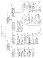
- FIG. 1 A summary of an aluminum gate PMOS (p-channel metal oxide semiconductor transistor) wafer fab process 40 is schematically shown in FIG. 1, illustrating major processing steps 41 through 73, as described in W.R. Runyan et al., Semiconductor Integrated Circuit Processing Technology, Addison-Wesley Publ. Comp. Inc., p.48, 1994. Each of these major processing steps typically include several sub steps. For example, a major processing step such as metallization to provide an aluminum layer by means of sputter deposition in a wafer fab chamber is disclosed in U.S. Pat. No. 5,108,570 (R.C. Wang, 1992). This sputter deposition process is schematically shown in sub steps 81 through 97 of process 80, see FIG. 2.
- a major processing step such as metallization to provide an aluminum layer by means of sputter deposition in a wafer fab chamber is disclosed in U.S. Pat. No. 5,108,570 (R.C. Wang, 1992). This sputter de
- FIGS. 1 and 2 show sequential wafer fab processes. It is also known to utilize wafer fab sub systems which provide parallel processing steps. Such sub systems typically include one or more cluster tools.
- a cluster tool as defined herein includes a system of chambers and wafer handling equipment wherein wafers are processed in the cluster tool chambers without leaving a controlled cluster tool environment such as vacuum.
- An example of a cluster tool is disclosed in U.S. Pat. No. 5,236,868 (J. Nulman, 1993) which employs a vacuum apparatus having a central chamber and four processing chambers.
- a wafer handling robot in the central chamber has access to the interior of each the processing chambers in order to transfer wafers from the central chamber into each of the chambers while keeping the wafers in a vacuum environment.
- wafers in the '868 cluster are first transferred for processing to a cleaning chamber, then to a PVD (physical vapor deposition) chamber, followed by transfer to an annealing chamber and subsequently to a degassing chamber, thus utilizing a sequential process.
- PVD physical vapor deposition
- critical processing characteristics such as the metal deposition rate
- the deposition system can be more readily maintained near desired levels when processing variables, such as the power input to the sputtering source, are adjusted in response to observed variations in the metal deposition processing characteristics.
- This requires in-situ measurement of processing characteristics, using for example a deposition rate monitor based on the optical attenuation of light passing through the deposition environment, thereby detecting the rate at which material is flowing from the deposition source to the deposition substrate, as described more fully in the '297 patent.
- a wafer fab includes a complex sequence of processing steps wherein the result of any particular processing step typically is highly dependent on one or more preceding processing steps.
- Processing and/or materials defects such as described above generally cause a reduced wafer fab yield, wherein the yield is defined as the percentage of acceptable wafers that are produced in a particular fab.
- the yield is defined as the percentage of acceptable wafers that are produced in a particular fab.
- In-process tests and monitoring of processing parameters are utilized to determine whether a given in-process product or process problem or defect indicates that intervention in the process run is necessary, such as making a processing adjustment or aborting the run. Consequently, product and process control techniques are used extensively throughout a wafer fab. When possible, yield problems are traced back to specific product or processing problems or defects to ultimately improve the yield of the wafer fab. High yields are desirable for minimizing manufacturing costs for each processed wafer and to maximize the utilization of resources such as electrical power, chemicals and water, while minimizing scrap re-work or disposal.
- SPC statistical process control
- SQC statistical quality control
- Control limits are typically set at a multiple of the standard deviation of the mean of the target value, such as for example 2 ⁇ or 3 ⁇ .
- the target value is derived from a test run or a production run which meets such wafer fab design criteria as yield, process control and product quality. SPC and SQC are considered synonymous when used in the above context, see R. Zorich at p. 464.
- Wafer fab tools such as chambers are typically controlled by a computer using a set of instructions which are generally known as a recipe for operating the process which is executed by the tool.
- a high degree of automation wherein various processes and metrologies are integrated, is difficult to achieve due to the complexity and inter dependency of many of the wafer fab processes, see for example Peter van Zandt, Microchip Fabrication, 3 rd ed., McGraw-Hill, pp. 472-478, 1997.
- a unit of semiconductor manufacturing equipment such as a wafer fab tool, commonly employs an on-board computer to identify and/or regulate equipment, processing or material parameters in connection with the tool and the manufacturing process.
- the communication interface between the on-board computer of the manufacturing unit and a host computer typically includes a protocol such as SECS II (SEMI Equipment Communication Standard).
- SECS II SEMI Equipment Communication Standard
- SECS II SEMI Equipment Communication Standard
- the limited data transfer capacity of this type of communication protocol imposes a restriction on communications between a computer and a tool, thereby limiting the types of data and the data transfer speed.
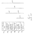
- Non-scheduled time 102 represents the time period wherein the equipment is not scheduled to be used, for example unworked shift.
- Unscheduled downtime 104 concerns time periods wherein the equipment is not in a condition to perform its intended function, e.g. during equipment repair.
- Scheduled downtime 106 occurs when the equipment is capable of performing its function but is not available to do this, such as process setup or preventive maintenance.
- Engineering time 108 concerns the time period wherein the equipment is operated to conduct engineering tests, for example equipment evaluation.
- Standby time 110 is a time period wherein the equipment is not operated even though it is in a condition to perform its intended function and is capable of performing its function, for example no operator is available or there is no input from the relevant information systems.
- Productive state 112 represents the time period wherein the equipment is performing its intended function, such as regular production and rework.
- Total time period 114 is the total time during the period being measured; this includes the six equipment states 102, 104, 106, 108, 110 and 112.
- Operations time 116 concerns the total time period of states 104, 106, 108, 110 and 112.
- Operations time 116 includes equipment downtime 118 consisting of states 104 and 106, and equipment uptime 120.
- Equipment uptime 120 includes engineering time 108 and manufacturing time 122 which consists of standby time 110 and productive time 112.
- FIGS. 4 and 5 provide more detailed schematic illustrations of the six equipment states shown in FIG. 3, see SEMI E10-96, at pp. 1-6.
- total time 114 consists of non-scheduled time 102 and operations time 116.
- Non-scheduled time 102 includes unworked shifts 130, equipment installation, modification, rebuilding or upgrading 132, off-line training 134 and shutdown or start-up time period 136.
- Operations time 116 as schematically illustrated in FIG. 5, consists of equipment downtime 118 and equipment uptime 120.
- Equipment downtime 118 consists of unscheduled downtime 104 and scheduled downtime 106.
- Unscheduled downtime 104 includes downtime for maintenance delay 140, repair time 142, changing consumables/chemicals 144, out of specification input 146 or facilities related downtime 148.
- Scheduled downtime 106 concerns downtime for maintenance delay 150, production test 152, preventive maintenance 154, changing consumables/chemicals 156, setup 158 or facilities related 159.
- Equipment uptime 120 consists of engineering time 108 and manufacturing time 122.
- Engineering time 108 includes process experiments 160 and equipment experiments 162.
- Manufacturing time 110 consists of standby time 110 and productive time 112.
- Standby time 110 includes time during which there is no operator 180, no product 182, no support tool 184 or when an associated cluster module is down 186.
- Productive time 112 concerns a time period during which there is regular production 190, work for a third party 192, rework 194 or an engineering run 196.
- the various equipment states as described in connection with FIGS. 3-5 provide a basis for communicating and evaluating RAM related equipment information in the semiconductor industry.
- RAM related equipment information includes topics which are well known to those of ordinary skill in the art such as: equipment reliability, equipment availability, equipment maintainability and equipment utilization, see for example SEMI E10-96 at pp. 6-11.
- the present novel techniques for data acquisition and management systems of semiconductor processing devices and wafer fabs provide the needed improvement in data acquisition, process control, quality, yield and cost reduction.
- a semiconductor fabricating tool and processing methods are provided wherein the tool includes a primary communication port and a secondary communication port.
- the tool also includes a sensor for sensing process, product and equipment parameters that are then communicated to a sensor data acquisition unit via the secondary port.
- the primary port is employed to communicate MES messages and queries to the tool.
- a method and apparatus for processing data from a wafer fab facility including a plurality of tools each having a primary and a secondary communication port as well as a sensor communicating with the secondary communication port.
- the facility additionally includes a host database and host computer as well as a data base management system and wafer fab management software. Tool operating instructions are executed employing legacy software communicating via the primary port of each tool. Sensor data are acquired via the secondary port of each tool.
- a computer executable process for operating a wafer fab management system derives a model for the system by defining wafer fabrication data structures, and by defining relationships between these structures.
- System configuration data are selected for operating the system.
- the configuration data are then adjusted according to a user input.
- Operational data are subsequently gathered when the system is activated.
- the operational data are gathered and then formatted to form updated data structures.
- a database management system is utilized to manage the gathered data and to insure consistency with the system data structures and the relationships between the data structures.
- a network distributed database for semiconductor fabricating is provided utilizing a plurality of semiconductor processing devices each having a tool including a primary and secondary data communication port.
- a network is provided for interconnecting the plurality of semiconductor devices and a data base management system.
- a computer executable data structure for operating one or more tools of a wafer fab.
- the data structure includes control system data.
- a data structure wherein data, organized in relational tables, are adapted for being accessed by one or more applications for semiconductor fabricating.
- a recipe manager application can access a recipe manager relational table or a recipe step relational table to add information to these tables, or to change the content of these tables.
- FIG. 1 is a flowchart schematically illustrating a prior art wafer fab process.
- FIG. 2 is a flowchart schematically illustrating a prior art wafer fab sputter metallization process.
- FIG. 3 is a stack chart schematically illustrating prior art equipment time states.
- FIG. 4 is a block diagram schematically showing prior art equipment time states of the stack chart illustrated in FIG. 3.
- FIG. 5 is a block diagram schematically showing prior art equipment time states of the stack chart illustrated in FIG. 3.
- FIG. 6 is a block diagram schematically illustrating a semiconductor processing device of the present invention.
- FIG. 7 is a block diagram schematically illustrating another semiconductor processing device of the present invention.
- FIG. 8 is a block diagram schematically illustrating an additional semiconductor processing device of the present invention.
- FIG. 9 is a block diagram schematically illustrating a network of instrumented tool subsystems and a database management system of the present invention.
- FIG. 10 is a block diagram schematically showing a networked, distributed database management system for managing a wafer fab management system of the present invention.
- FIG. 11 is a block diagram illustrating hierarchical relationships between data objects of a computer executable process for operating a wafer fab system of the present invention.
- FIG. 12 is a block diagram illustrating a relationship between functional modules of a system for managing a wafer fab system of the present invention.
- FIG. 13 is a functional database schema diagram illustrating relationships between elements of a database of the present invention.
- FIG. 6 shows a semiconductor processing device 600, employing an EDAS (enhanced data acquisition system) of the present invention.
- the novel EDAS is adapted for monitoring, i.e. observing, analyzing and reporting, semiconductor wafer or IC (integrated circuit) fabricating or processing tools, hereinafter referred to as tools. These tools include wafer fab chambers such as etch and deposition chambers, as well as wafer and wafer cassette handling equipment.
- the novel EDAS includes: (1) a DB (database) for storing information concerning equipment, processes and wafer data, (2) software adapted for performing data acquisition or collection, SPC analysis and historical reporting, and (3) a UI (user interface) for obtaining information about individual tools and factory wide equipment.
- DB database
- Software for controlling and executing the EDAS of the present invention provides: (1) data collection and storage of equipment data, (2) process and equipment monitoring, including real time and correlation with historical data, particularly where these data are correlated with the relevant wafer lot history file, and (3) control limits detection of single processing events including alarmed responses.
- Tools adapted for employing EDAS include two communication ports.
- a primary communication port provides an interface for communicating conventional MES (manufacturing execution systems) messages and data.
- the primary port utilizes a conventional equipment standard, such as SECS II (SEMI Equipment Communication Standard II).
- SECS II SEMI Equipment Communication Standard II
- the primary port includes a serial port operating at a maximum baud rate of about 19200.
- a SECS II primary port provides an interface protocol that supports conventional, also known as standard, SECS II messages using any of the technologies that are well known to those of ordinary skill in the art.
- a novel secondary port provides an interface for communicating EDAS data through an interface protocol that supports conventional SECS II messages as well as custom SECS II messages adapted for communicating EDAS data.
- the secondary port operates at a higher baud rate than the primary port.
- the secondary port includes a serial port operating at a maximum baud rate of about 38400.
- the novel secondary port supports messages using the HSMS (high speed message service) protocol.
- device 600 includes a tool 610, a primary communication port 612 for communicating conventional MES messages and data 614, a novel secondary communications port 616 providing an interface between tool 610 and a novel EDAS acquired data environment 618.
- An information processing and analyzing environment 624 is linked through a link 622 to the EDAS acquired data environment 618.
- the device also includes a tool DB 620.
- device 600 can be equipped with a decision making environment 626 which is optionally adapted for communication with a response environment 628.
- a dedicated mass storage 630 is linked to information processing and analyzing environment 624.
- network access is provided through one or more network serial ports 632 communicating with a network 634.
- environment includes an aggregate of technologies, methods and/or devices which provide a resource for acquiring data, data structures or information and which, optionally, can interact with the acquired data, data structures or information.
- An environment as used herein includes a computer environment.
- computer environment includes computer software and/or hardware which provides a resource for acquiring data, data structures or information and which can interact with the acquired data, data structures or information.
- Tool 610 includes such controllers (not shown) and inputs as are necessary to produce the desired wafer or IC structures, for example microprocessors including on-board computers, computer operated software as well as mechanical/electrical controllers including switches and electrical circuits employing for example a variable resistor such as a potentiometer. These controllers operate or control various tool processes and operational functions such as gas flow and wafer handling.
- One or more sensors are provided in connection with tool 610 to sense and report process, product or equipment parameter data.
- Operational instructions, such as MES instructions and queries, for tool 610 can be provided to tool 610 by means of tool DB 620 or by means of MES messages 614 utilizing for example an MES input device such as a keyboard or a GUI (graphics user interface) 615, a pointing device such as a light pen or a mouse, an OCR (optical character reader), voice instructions employing for example voice recognition software, and a removable data storage medium or device, using any of the methods and technologies that are well known to those of ordinary skill in the art.
- operational instructions can also be provided to the tool by accessing the tool on-board processor or by conventional data entry techniques.
- Operational instructions may include specific settings for equipment parameters, for example the closing or opening of a valve. These instructions can also include processing instructions, for example specifying a processing recipe or specifying wafer lot numbers or specifying the beginning or ending of a processing sequence.
- Input messages, queries or data for novel EDAS can be provided to tool 610 by means of an input device 642 and/or tool DB 620, via secondary port 616.
- Suitable examples of input device 642 include a keyboard, a GUI, a pointing device such as a light pen or a mouse, an OCR, voice instructions, and a removable data storage medium or device such as a removable digital or optical data computer disk or tape.
- An EDAS of the present invention typically employs two input devices 615 and 642. It will be understood that these two devices can be merged (not shown) into one device having the separate functionalities of device 615 for MES input and device 642 for EDAS input of messages and queries.
- Tool 610 sensors can provide EDAS data including sensor data, which are communicated through secondary port 616, see FIG. 6, and are acquired in EDAS acquired data environment 618 of device 600.
- This environment includes mass storage devices and/or communication links for receiving and then communicating the data to information processing and analyzing environment 624.
- Dedicated mass storage device 630 provides a storage medium for historical data, including wafer lot history files, and process or product control limits.
- a reporting environment 636 is adapted for providing reports in for example hard copy or by means of a display on a monitor. These reports include alphanumeric data and graphical representations.
- Links such as link 622 include hard wire connections, conductive surfaces, optical components and conventional wireless communication techniques.
- Information processing and analyzing environment 624 of novel semiconductor processing device 600, shown in FIG. 6, utilizes methodologies such as are well known to those of ordinary skill in the art, to determine process control limits meeting the design and yield criteria for producing semiconductor wafers and IC structures.
- the control limits are statistically derived using one or more processing and/or in-process product parameters which are indicative of a process meeting the design and yield criteria for fabricating the structure.
- environment 624 acquires process and/or product metrology information from production runs for producing these structures, using the same parameters as were used to establish the control limits. An analysis is then performed in this environment to determine whether the process or product is produced within the control limits.
- Environment 624 typically employs a data processor, such as a microprocessor to perform the data processing requirements of this environment.
- SPC methodologies suitable for use in information processing and analyzing environment 624 of the present invention include control chart methodologies and Pareto charts.
- a Pareto chart is a bar chart representation that displays a ranking of the number of occurrences of a particular defect as compared with the cumulative number of occurrences of all defects and the number of occurrences of each of the other defects or problems.
- control limits are typically determined following the collection of a statistically significant number of data, which are relevant to an important or critical parameter indicative of the process operating as designed and resulting in an acceptable yield.
- a suitable parameter for a process carried out in tool 610 can include sputter power in a sputter deposition process, gas flow rate and/or pressure, and particle contamination in the chamber environment.
- Metrology data measuring these parameters at specific intervals provide the input for the determination of control limits.
- metrology data concerning in-situ product testing can be used in a similar way. For example using the technology disclosed in the '989 patent for measuring the sheet resistance of an electrically conductive film on a semiconductor substrate in-situ, while maintaining the substrate within the vacuum environment of the semiconductor process apparatus. The data which are obtained from the process while running in control, i.e. within operational specification and/or yield, are then computed to determine the process control limits using statistical methods which are well known to those of ordinary skill in the art. Subsequent production runs are then analyzed using metrology data of the same processing or in-situ product parameters as were used to determine the control limits.
- Information processing and analyzing environment 624 of novel semiconductor processing device 600 is adapted for comparing real time data with historical data or for performing chamber matching analysis, utilizing SPC methodologies and providing numerical and/or graphical representations through for example reporting environment 636.
- decision making environment 626 determines that the process is operating within the predetermined control limits, there is no intervention. However, when analysis shows that the process is outside the control limits, a response such as an alarm or an out of control limits indicator can be activated, responsive to a predetermined alarm condition e.g. being outside the control limits. It is also contemplated to initiate processing intervention through response environment 628, for example by aborting the processing sequence if the process is not operating within the control limits. Decision making environment 626 typically employs a microprocessor.
- novel semiconductor processing device 600 includes a novel product or a novel apparatus comprising one or more digitally coded equipment, processing or product data structures including the novel EDAS.
- Tool 610 can be equipped with one or more peripheral devices 644, such as pumps or chillers.
- the peripheral devices can transmit data to network 634 via a network port 646.
- FIG. 7 shows a semiconductor processing device 700 of the present invention.
- This device includes a tool 702 having one or more sensors (not shown) providing EDAS sensor data that are communicated through a novel secondary port 704, to a data acquisition subsystem 706 including an EDAS data acquisition unit 708, an optional digital data processing unit 710, a tool DB 712 and a network connection 714.
- Secondary port 704, EDAS data acquisition unit 708 and tool DB 712 of device 700 are similar to secondary port 616, EDAS acquired data environment 618 and tool DB 620 respectively of device 600 as described in connection with FIG. 6.
- EDAS information, messages or queries can be communicated from EDAS input device 705 or tool DB 712 to tool 702 via secondary port 704, while input device 733 can be utilized to communicate MES messages to tool 702 via primary port 730.
- Input devices 705 and 733, MES messages 732 and primary port 730 are similar to the corresponding units described in connection with device 600.
- Digital data processing unit 710 for example employing a CPU, can be employed to convert or process the data to a format suitable for processing by a data processing subsystem 716 or for transmission to a network.
- Acquired EDAS data are communicated from EDAS data acquisition unit 708 to EDAS data processing unit 720.
- the EDAS data are processed and analyzed in unit 720 resulting in processed EDAS data, using methods such as those described in connection with the information processing and analyzing environment 624 of device 600, shown in FIG. 6.
- unit 720 is adapted for making product or processing related decisions to, for example, activate an alarm if the process is not operating within control limits, as described in connection with decision making environment 626 and response environment 628 of device 600.
- Mass data storage device 722 of sensor data processing unit 720 can provide for example historical data, including wafer lot history files, or process control limit data.
- Reporting unit 724 is adapted to, for example, display or print the results obtained from processing and analyzing the EDAS data, similar to reporting environment 636 of device 600, shown in FIG. 6.
- novel semiconductor processing device 700 is utilized to determine the endpoint of a wafer etching process. Upon reaching the etch process endpoint, the etch step is completed and must be terminated. See for example US. Pat. No. 5,910,011 (Cruse) for a description of this process. In order to make an endpoint determination the output of one or more sensors must be monitored to make this determination. Generally, this task requires the use of a mass storage device to support processing the sensor data.
- Data acquisition subsystem 706 of device 700 is implemented on a Microsoft NT type operating system using a PC processor operating at a 400 MHz clock rate.
- the PC processor includes three X GB hard disks for storage of program and data.
- the digital data processing unit 710 and the mass storage device 712 are both supplied by the PC processor and its hard disks.
- the network connection 714 is provided by an Ethernet card and compatible software installed at the PC.
- Data processing unit 710 and a portion of tool DB 712 include a stored program that runs on data processing unit 710 and configures unit 710 to process and format the sensor data acquired in EDAS data acquisition unit 708, and to then store sensor data on tool DB 712.
- the configuring software is stored on one of the hard disks, running on the PC, and organizing the PC to receive EDAS data from tool 702 via secondary port 704 in EDAS data acquisition unit 708.
- the configuring software also processes and formats the data and stores predetermined data on one of more of the hard disks.
- the predetermined data can be communicated via network connection 714.
- Data processing subsystem 716 comprises an endpoint processing subsystem 716 that receives EDAS acquired data via data link 718.
- Data processing unit 720 comprises a dedicated endpoint data processor that is running an endpoint determination application.
- the dedicated processor 720 is supported by a mass storage device 722, for example an 8 GB hard disk.
- Communication between endpoint processor 720 and data acquisition subsystem 706 is provided via data link 718.
- endpoint processing subsystem 716 determines when the endpoint has occurred, and that conclusion is then communicated to data acquisition subsystem 706 via link 718.
- device 700 can also be utilized to initiate an alarm or alert an equipment operator to indicate that the endpoint has been reached.
- Device 800 includes a tool 802 having one or more sensors (not shown).
- the device also includes a primary port 804, a secondary port 806, a data acquisition subsystem 808, a sensor data processing subsystem 810, a data link 812 and a network connection 814, wherein the primary and secondary ports are similar to the corresponding ports of devices 600 and 700.
- the data acquisition subsystem 808 includes an MES data acquisition unit 816 for acquiring data for example concerning the on-line status of tool 802, and an EDAS data acquisition unit 818, for example acquiring tool sensor EDAS data for SPC analysis.
- a digital data processing unit 820 and a tool database 822 are also included in data acquisition subsystem 808.
- Digital data processing unit 820 is adapted for processing data from MES acquisition unit 816 and from EDAS data acquisition unit 818.
- EDAS data acquisition unit 818 and tool DB 822 of device 800 are similar to EDAS data acquisition unit 708 and tool DB 712 respective of device 700.
- Input device 826 of processing device 800 shown in FIG. 8 is adapted for entry of MES inputs and for entry of EDAS inputs, thereby providing a combination of the functions of MES input device 733 and EDAS input device 705 of processing device 700 illustrated in FIG. 7.
- a sensor data processing subsystem 810 communicating with subsystem 808 via link 812, includes a dedicated EDAS data processing unit 828 and a dedicated mass storage device 830, similar to EDAS data processing unit 720 and dedicated mass storage 722 of device 700 shown in FIG. 7..
- the MES data from MES data acquisition unit 816 can be processed by data processing unit 820.
- the software application that runs on the data processing unit 820 includes a module for handling the MES data, and for making the MES data a part of tool DB 822.
- Device 800 includes a reporting unit 824 driven by sensor data processing subsystem 810.
- Reporting unit 824 of device 800 is similar to reporting environment 636 of device 600, illustrated in FIG. 6, except that reporting unit 824 is additionally adapted for reporting MES related data.
- the reporting unit, data entry device, and compatible software running on data processing unit 820 permits the tool operator to control the configuration and the operation of tool 802 and data acquisition subsystem 808 using familiar interface devices.
- Semiconductor processing device 800 also includes a peripheral device 834, such as a pump or a chiller. Peripheral device 834 of tool 802 can receive instructions or provide operation data via a network.
- a further embodiment of the present invention provides a network system 900 of semiconductor processing devices.
- Network system 900 schematically illustrated in FIG. 9, includes a plurality of semiconductor processing devices exemplified by devices 902, 904 and 906, a DBMS (database management system) 908, and a network 910 interconnecting the separate semiconductor manufacturing devices and the DBMS.
- the resulting system forms a network distributed database that includes all the data in all the digital storage devices.
- DBMS 908 is configured as a network server and the individual semiconductor processing devices 902, 904, and 906 are configures as network clients.
- Semiconductor processing devices suitable for use in the present invention include semiconductor processing devices 600, 700 and 800, illustrated in FIGS. 6, 7 and 8 respectively.
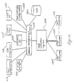
- FIG. 10 shows a system 1000 for managing a wafer fabrication facility.
- System 1000 includes a wafer fab component 1002 having a tool-1 1004, a tool-2 1006, a tool-3 1008 and a tool-n 1010, the tools having primary ports 1012, 1014, 1016 and 1018 respectively, secondary ports 1042, 1044, 1046 and 1048 respectively, a host computer 1020, and a host database 1022.
- Host computer 1020, host database 1022 and primary ports 1012-1018 form a legacy system within wafer fab component 1002.
- the primary and secondary ports of system 1000 are similar to the corresponding ports of device 600 illustrated in FIG. 6.
- each of tools 1 through 2 includes one or more sensors (not shown) for providing EDAS data.
- System 1000 also includes a database management system 1024, wafer fab management software 1026, a network interface 1028, a network 1030, EDAS tool subsystems 1032, 1034, 1036 and 1038, and a non-tool client computer 1040.
- Each EDAS tool subsystem receives tool sensor EDAS data via its secondary port.
- each EDAS tool subsystem includes an EDAS data gathering front end 1050, 1052, 1054 and 1056, a tool client 1058, 1060, 1062 and 1064 and a mass storage device 1066, 1068, 1070 and 1072 each providing a DB for each of the tools.
- Tool clients 1058-1064 for tool 1, 2, 3 and n respectively provide a functionality similar to the functionality of optional data processing unit 710 and EDAS data processing subsystem 716 of device 700 shown in FIG. 7.
- a reporting unit similar to reporting unit 724 of device 700 can be provided to each of EDAS tool subsystems 1032-1038.
- a similar reporting unit can be provided to non-tool client computer 1040.
- An input device for entering EDAS messages and queries similar to EDAS input device 705 of processing device 700 (FIG. 7), can be provided to each of EDAS tool subsystems 1032-1038 and to non-client computer 1040.
- EDAS messages and queries can also be entered into tools 1, 2, 3 and n by means of DB parts 1, 2, 3 and n, similar to the input system of device 700 and wherein tool DB 712 is adapted for entering EDAS messages.
- the present invention provides functionality and database management that is added to the legacy system of wafer fab component 1002, shown in FIG. 10, through database management system 1024 and wafer fab management software 1026 that are integrated with host computer 1020 and host DB 1022 to form a compatible system utilizing the primary ports 1012 - 1018 for managing wafer fab component 1002 by means of operating instructions, such as MES instructions, provided through host computer 1020.
- operating instructions such as MES instructions
- Duplicate values of MES instructions are synchronized between host (legacy) database 1022 and the added database management features 1024.
- host computer 1020 is a work station having one or more mass storage devices such as host DB 1022.
- database management 1024, wafer fab management software 1026, and network interface 1028 features reside within work station 1020, while the database and data structures reside partly on host DB 1022 and partly on mass storage devices 1066-1072 of tool subsystems 1032-1038
- databases of system 1000 are synchronized to transfer copies of the duplicated information from wafer fab 1002 to database 1024.
- the present invention includes EDAS data, including sensor data, acquisition via secondary ports 1042, 1044, 1046 and 1048, and EDAS tool subsystems 1032,1034,1036 and 1038, respectively.
- the EDAS data acquisition of the present invention is employed to gather information not available through primary ports 1004, 1006, 1008 and 1010 of wafer fab component 1002.
- management system 1000 (FIG. 10) described above implements a host computer 1020 and network interface 1028 as a network server, and implements each EDAS tool subsystem 1032 - 1038 as a network client.
- wafer fab management system 1000 includes one or more non-tool client computers 1040 that are used to extend a user interface throughout the networked system, wherein the non-tool client computer provides remote access to wafer fab component 1002, host computer 1020, host database 1022 and EDAS tool subsystems 1032-1038.
- wafer fab management software 1026 is partitioned between host work station 1020 and the individual EDAS tool subsystems 1032 - 1038. This partition is possible because some management tasks relate to EDAS data acquisition that are placed in the EDAS context of EDAS subsystems 1032-1038, rather than attempting to control EDAS data gathering via a more limited network connection such as network 1030.
- the acquired EDAS data of wafer fab management system 1000 is maintained within individual EDAS tool subsystems 1032 - 1038, wherein the acquired EDAS information of each tool is stored on the tool subsystem mass storage devices 1066-1072.
- the database management function 1024 is also partitioned between the host work station 1020 and the tool subsystem data processing units 1058-1064. Database management function 1024 is partitioned because some portions of the database are more closely related to EDAS data acquisition, while the need to access that data from host work station 1020 can be handled via network connection 1030.
- those portions of the database management system most closely related to EDAS data collection are placed in a partition running on the tool subsystems' data processing units 1058-1064, and using the tool subsystems' mass storage device 1066-1072.
- the resulting distribution of portions of the system database among the host computer mass storage 1022 and the tool subsystems' mass storage devices 1066-1072 defines a networked, distributed database management system.
- EDAS tool subsystems 1032 - 1038 include a wafer fab process endpoint determination subsystem interconnected with the tool subsystems via a primary port.
- the endpoint determination subsystem can be adapted for utilizing a plurality of tool sensors providing a plurality of EDAS sensor data, and correlating these data to improve the accuracy of the endpoint determination.
- Database management system 1024 includes the ability to analyze the data stored in the distributed database and to prepare reports in a number of formats including equipment states such as the SEMI E10-96 equipment states described in connection with FIGS. 3 - 5.
- the present invention provides a novel automatic reporting feature wherein E-10 states and for example equipment RAM are available to the operator at any time via a user interface. This feature is adapted for making tool maintenance schedules, tool diagnostic procedures and spare parts inventories available to the user at any time via a user interface using the distributed database of wafer fab management system 1000.
- Wafer fab management software 1026 implements a user interface feature permitting management system 1000 to be responsive to appropriate user inputs for modifying the system configuration.
- the wafer fab management software includes a set of security rules governing user access to the sensor data, distributed database and to the E10 equipment states. These security rules permit the users to be classified according to a predetermined hierarchy such that each user has an assigned security level within the hierarchy, and access is permitted under the security rules to the levels of the hierarchy on a need-to-know basis.
- the database management function 1024 of novel management system 1000 provides the techniques necessary for analyzing selected data within the distributed database according to a predetermined plan.
- the selected data includes historical system data, data relating to a single tool, data relating to a single wafer, or to a single production run.
- the report generating features of the database management function 1024 are useful for reporting the results of such analysis via a user interface. Such reports include for example SPC related reports, tool performance data and chamber matching results.
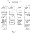
- FIG. 11 shows a novel hierarchical relationship system 1100 including hierarchical relationships between data objects of a computer executable process for operating one or more tools of a wafer fabrication system.
- An example of a computer executable process for a wafer fab includes the combination of DBMS 1024, wafer fab management software 1026, network interface 1028 and host computer 1020 of device 1000, depicted in FIG. 10.
- the diagram shown in FIG. 11 illustrates the types and subtypes of data objects (also referred to simply as "data") that the process gathers, creates, and handles while operating the tool. The diagram begins at the top with reference to the "entire set of control system data".
- the system configuration data 1102 includes tool configuration data and parameters ("syscons” for “system constants”) 1110, tool component device configuration data and parameters (also referred to as syscons) 1112, users and groups access rights data 1114, and data collection configuration data 1116.
- the systems parameters 1104 include SVID (status variable identifier) data 1118, operational syscons data 1120 ("syscons” is used interchangeably in a number of contexts; distinctions will be made when necessary to insure clarity of meaning), data and events data 1122.
- Process control data 1106 includes sequences 1124, recipes 1126, and SPC/APC (advanced process control)/FD (fault detection) rules 1128.
- the collected data 1108 includes event log data 1130, wafer history data 1132, process data 1134, and SPC/APC/FD results data 1136.
- one or more tools including a first communication port and a second communication port similar to primary and secondary ports 612 and 616 respectively of processing device 600, illustrated in FIG. 600. It is further contemplated to communicate process control data 1106, shown in FIG. 11, via the primary port to the tool and to communicate collected data from a tool sensor (not shown) to a data gathering unit or environment via the secondary port.
- control system uses and collects the data illustrated in FIG. 11.
- the various types of data have much in common with each other.
- Table I describes some of the qualities these diverse data types share.
- the present invention is adapted for providing functionality that supports some or all the above data properties.
- the most suitable means for employing this functionality is to structure the entire set of control system data 1101 (FIG. 11) as a database.
- a database when viewed as a data storage repository, includes an entire set of system data, their relationships and constraints on them that define correct database states. Databases are supported by a database management system (DBMS) which is software that provides services for accessing a database, while supporting data persistence, validity, consistency, non-redundancy, security, and the possibility to be shared. Database provides easy, powerful and flexible data storing, filtering, and searching. It simplifies data classification, comparison, and finding repeatability and irregularities in data.
- DBMS database management system
- Database is not just a convenient way to control system data handling, it also significantly decreases the size of code. As a result, software reliability and fault-tolerance increases, and future code modifications become simpler to implement.
- DBMS provides means for implementation of a set of separate applications each supporting a part of the control system functionality. These applications access parts of database schema while sharing database data.
- FIG. 12 shows a computer implemented control system 1200 for semiconductor fabricating.
- This system includes a database 1202, a database management system (DBMS) 1204, a data collection engine (data gathering) 1206, EDAS tool subsystems 1208, 1210, 1212 (similar to EDAS tool subsystems 1032-1038 of wafer fab management system 1000, illustrated in FIG. 10, a tool configuration application 1214, a user configuration application 1216, a wafer history application 1218, an event log application 1220, a recipe manager application 1222, an SPC/APC/FD application1224, and a data collection application 1226.
- the database and the applications reside on a dedicated PC, such as an NT front end.
- control system 1200 The use of a database and database applications provide novel properties and features to the control system 1200. Among these are the following: (1) more convenient and easy data access because of support of data relationships and other data features discussed above; (2) remote access to data; (3) the ability to configure the tool, to edit recipes, to analyze collected data, etc., not only when legacy is active, but also when the tool is inactive,; and (4) easier tools integration and an open interface for other software.
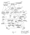
- FIG. 13 shows a functional database schema 1300 wherein data describe interrelated physical entities. Data are organized in relational tables, represented as rectangles in FIG. 13.
- Functional database schema 1300 includes the following tables: chamber model 1302, chamber variance 1304, current subsystem configuration 1306, subsystem 1308, device 1310, current device configuration 1312, soft version 1314, syscon bit 1316, syscon 1318, category 1320, parameter - SVID 1322, event 1324, event log 1326, unit 1328, event source 1330, user group 1332, wafer visit 1334, wafer history event log 1336, recipe 1338, step 1340, user 1342, application 1344, metrics 1346, trigger 1348, recipe summary 1350, step summary 1352, lot type 1354, session 1356, signal 1358, session log 1360, signal log 1362, process data description 1364, process data 1366, lot 1368, and wafer 1370.
- Each application of computer implemented control system 1200 accesses one or more tables of functional database schema 1300 (FIG. 13).
- the recipe manager 1222 of system 1200 provides recipe editing and searching of a specific recipe using some criteria, such as chamber model, user-creator, specific value of recipe parameter, etc.
- the recipe manager 1222 puts data directly into recipe 1338, and into recipe step 1340.
- These tables are used in turn by the wafer history application 1318 along with the tables for lot 1368, wafer 1370, recipe summary 1350, wafer visit 1334, wafer history event log 1336, and the lot type 1354.
- the recipe summary 1350 is logged, the user can view the recipe's details.
- Some tables of schema 1300 can be modified (edited) by the user, while others define "dictionaries".
- Dictionaries are tables that contain dictionary information and are identified with an asterisk in FIG. 13. Dictionary information is shipped as a part of release software and may not be modified. "Dictionary" information describes predefined knowledge about tool-lot types (for instance, processing engineering), the tool's subsystems (Mainframe, Chamber A, etc.) chamber models and variances, devices that may be configured to these types of chambers, and the like. Data separation allows the applications to work without changes in their code when new information appears. For instance, a new software baseline supports a new chamber variance. In this case, dictionaries are provided with pre-defined new records in corresponding tables (chamber variance and chamber model, if required). No change is needed in recipe manager code because there is no difference between a new record and old records.
- the data have complex relationships with several many-to-many ties.
- the tables themselves also have complex structure. This is especially true for the tables connected with configuration data.
- a special dictionary structure has been invented.
- two dedicated fields function as abstract "parent" and "child” rather than representing specific chamber or device attributes.
- Parent and child may describe any attribute of any entity.
- the attribute that was used as a child in the previous record may be the parent in the next record. It gives the possibility to include another entity with all its attributers in the same table.
- the dictionary is linked with a special table, its records describing correspondence of dictionary records to each other. This allows implementation of multidimensional hierarchy. This hierarchy encapsulates all functionality of the usual 2D-tree and provides a flexible mechanism that allows browsing the hierarchy from different points of view while starting from different points.
- a database approach helps to fulfill current demands and a higher level of tools integration and statistical process control.
- Data-oriented functionality (comparison, classification, search, etc.) may be implemented in an easier way and be more convenient for the user.
- the database gives the possibility to implement new functionality regardless of the prior art software design. This makes possible the implementation of SPC/APC/FD that integrates smoothly with conventional code.
- the process defines data structures and relationships between the defined data structures (the database schema of FIG. 13) for defining the wafer fabrication system.
- the process gathers system configuration information (1102 of FIG. 11), such as which tools are on-line and ready for operation, for selecting an appropriate model (1106 of FIG. 11) according to the tools actually present and operational.
- the process includes applications for informing a system operator of the existing system configuration, and response to operator inputs for altering the system configuration by activating/deactivating specific tools and peripheral devices.
- the process also includes a recipe (1126 of FIG. 11) permitting the model to be used to control the wafer fabrication system to obtain a desired result, e.g., the production of a specific integrated circuit type.
- Control of the system is achieved in one of two alternative ways.
- the process generates alarms and reports permitting an operator to determine what intervention is required, and to manually effect the required control actions, such as shutting down a sub-process or adjusting a gas valve.
- the process generates control signals that are transmitted to a tool or a peripheral device and are converted at the tool or peripheral device into electro-mechanical actions that effect the required control in a closed-loop manner.
- the process of the present invention initiates operation of the wafer fabrication system according to the recipe, and then gathers operational data (1108 of FIG. 11) from the wafer fabrication system tools and peripherals while the etching process and related processes continue.
- the computer executable process formats and processes the gathered data to form the database defined data structures.
- the process uses the model and the formed data structures to control the wafer fabrication process, and continues gathering, modeling and controlling as the etch and related processes continue according to the recipe.
- the process determines when a process endpoint is reached, and then uses one of the alternative control methods described above to terminate the process and to begin subsequent processes according to the appropriate sequences (1124 of FIG. 11).
- the computer executable process is partitioned between a first computer (908 of FIG. 9) on which the bulk of the process runs, and a second computer that handles the data gathering and processing operations on a plurality of such second computers, such as subsystems 902 - 906 (FIG. 9) and providing a communication function (e.g., the network 910 of FIG. 9) permitting the first computer of DBMS 908 to receive the gathered, formatted and processed operational data from the second computer 902.
- the process extends the boundaries of the physical database beyond the single database (1202 of FIG. 12).
- the second computer (902 of FIG. 9) stores the data gathered at the tool-1 subsystem, and forwards to the first computer 908 only that data needed for the immediate needs of the process.
- This specific embodiment defines a networked, distributed database.
- the process extends the partition to include a plurality of second computers (902 - 906 of FIG. 9), each gathering data from a specific tool or set of tools and related peripherals.
- each such second computer executes a copy of the same partition of the overall computer executable process.
- the partition provides for the gathering, formatting, processing, and storing of data from the specific tool set.
- the communication function is extended to handle a plurality of data gathering streams from tool subsystems 902 -906.
- a novel fab tool employing the primary and secondary data communication ports of the present invention provides improved data communications with tool sensors because the ports enable the tool sensor to communicate messages, queries and data at a higher rate than a conventional tool equipped with a conventional (standard) communication port.
- the secondary port provides tools of the present invention with a novel data channel in addition to the conventional (standard) data channel, i.e. the primary port.
- the secondary port is particularly advantageous when it is capable of operating at a significantly higher baud rate than a conventional primary port.
- the partition running on the first computer 908 includes a database management system application 908 for managing all the data gathering streams and insuring that the gathered data is consistent with the defined data structures.
- the database management system 908 handles the responsibility for building the defined data structures from the gathered data streams 902 - 906.
- the database management system 908 is assigned total responsibility for insuring that all data structures for the model are consistent with the defined structures, and that all relationships between the structures are enforced, and for protecting the data form improper access.
- a partition of the database management function is executable by the second computers and has the same responsibility with respect to gathered data stored at each second computer.
- the communication function (network 910 of FIG. 9) is extended to permit the database management system to include the data stored at each second computer in a -distributed database.
- the process is stored on a computer readable medium, such as a CD-Rom, DVD-ROM, and the like.
Landscapes
- Physics & Mathematics (AREA)
- General Physics & Mathematics (AREA)
- Engineering & Computer Science (AREA)
- Automation & Control Theory (AREA)
- General Factory Administration (AREA)
- Drying Of Semiconductors (AREA)
Applications Claiming Priority (2)
| Application Number | Priority Date | Filing Date | Title |
|---|---|---|---|
| US561440 | 2000-04-28 | ||
| US09/561,440 US6952656B1 (en) | 2000-04-28 | 2000-04-28 | Wafer fabrication data acquisition and management systems |
Publications (2)
| Publication Number | Publication Date |
|---|---|
| EP1150187A2 true EP1150187A2 (fr) | 2001-10-31 |
| EP1150187A3 EP1150187A3 (fr) | 2005-03-02 |
Family
ID=24241987
Family Applications (1)
| Application Number | Title | Priority Date | Filing Date |
|---|---|---|---|
| EP01104512A Withdrawn EP1150187A3 (fr) | 2000-04-28 | 2001-03-02 | Systèmes de gestion et d'acquisition de données de fabrication de galettes |
Country Status (5)
| Country | Link |
|---|---|
| US (1) | US6952656B1 (fr) |
| EP (1) | EP1150187A3 (fr) |
| JP (1) | JP2002015969A (fr) |
| KR (1) | KR100808341B1 (fr) |
| TW (1) | TW473802B (fr) |
Cited By (14)
| Publication number | Priority date | Publication date | Assignee | Title |
|---|---|---|---|---|
| WO2003050628A3 (fr) * | 2001-12-12 | 2003-11-27 | Advanced Micro Devices Inc | Procede et appareil pour ordonnancer les lots de fabrication sur la base des mesures de sante des lots et des outils |
| EP1349091A3 (fr) * | 2002-03-27 | 2003-12-17 | Kabushiki Kaisha Toshiba | Système, méthode et programme pour la fabrication de masque LSI |
| WO2003103024A3 (fr) * | 2002-05-29 | 2004-04-01 | Tokyo Electron Ltd | Procede et appareil de controle des performances d'un outil |
| WO2004079465A1 (fr) * | 2003-03-01 | 2004-09-16 | Applied Materials, Inc. | Base de donnees d'interface de communications destinee a un appareil de diagnostic electronique |
| EP1519255A3 (fr) * | 2003-09-23 | 2005-04-27 | Oerlikon Contraves Ag | Appareil, méthode et produit de programme informatique pour la gestion centralisée d'une pluralité de systèmes électromécaniques |
| US7283255B2 (en) | 2002-02-06 | 2007-10-16 | Cyberoptics Semiconductor, Inc. | Wireless substrate-like sensor |
| CN100463104C (zh) * | 2005-03-29 | 2009-02-18 | 东京毅力科创株式会社 | 基板处理装置、历史信息记录方法、记录程序及记录系统 |
| US7778793B2 (en) | 2007-03-12 | 2010-08-17 | Cyberoptics Semiconductor, Inc. | Wireless sensor for semiconductor processing systems |
| US7804306B2 (en) | 2006-02-21 | 2010-09-28 | CyterOptics Semiconductor, Inc. | Capacitive distance sensing in semiconductor processing tools |
| US7893697B2 (en) | 2006-02-21 | 2011-02-22 | Cyberoptics Semiconductor, Inc. | Capacitive distance sensing in semiconductor processing tools |
| US8155770B2 (en) | 2009-03-31 | 2012-04-10 | Globalfoundries Inc. | Method and apparatus for dispatching workpieces to tools based on processing and performance history |
| EP2363773A3 (fr) * | 2010-02-26 | 2013-11-20 | General Electric Company | Systèmes et procédés de surveillance de l'état des équipements dans une installation d'alimentation électrique |
| US8823933B2 (en) | 2006-09-29 | 2014-09-02 | Cyberoptics Corporation | Substrate-like particle sensor |
| CN112947146A (zh) * | 2021-01-27 | 2021-06-11 | 许昌学院 | 一种高效工业机器人智能采集控制系统 |
Families Citing this family (363)
| Publication number | Priority date | Publication date | Assignee | Title |
|---|---|---|---|---|
| US7280883B2 (en) * | 2001-09-06 | 2007-10-09 | Dainippon Screen Mfg. Co., Ltd. | Substrate processing system managing apparatus information of substrate processing apparatus |
| US6776872B2 (en) * | 2002-03-05 | 2004-08-17 | Hitachi, Ltd. | Data processing apparatus for semiconductor processing apparatus |
| TWI286785B (en) * | 2002-03-29 | 2007-09-11 | Tokyo Electron Ltd | Method for interaction with status and control apparatus |
| AU2003253594A1 (en) * | 2002-04-23 | 2003-11-10 | Tokyo Electron Limited | Method and apparatus for simplified system configuration |
| TWI240179B (en) * | 2002-06-06 | 2005-09-21 | Taiwan Semiconductor Mfg | Parsing method for recipe data |
| AU2003281422A1 (en) * | 2002-07-03 | 2004-01-23 | Tokyo Electron Limited | Method and apparatus for automatic sensor installation |
| CN100375086C (zh) * | 2002-07-03 | 2008-03-12 | 东京电子株式会社 | 用于动态传感器配置和运行时间执行的方法和设备 |
| US20050004781A1 (en) * | 2003-04-21 | 2005-01-06 | National Gypsum Properties, Llc | System and method for plant management |
| US7375035B2 (en) * | 2003-04-29 | 2008-05-20 | Ronal Systems Corporation | Host and ancillary tool interface methodology for distributed processing |
| TWI283817B (en) * | 2003-05-30 | 2007-07-11 | Tokyo Electron Ltd | Method of operating a process control system and method of operating an advanced process control system |
| US20050010311A1 (en) * | 2003-07-10 | 2005-01-13 | Barbazette Christopher J. | Data collection and diagnostic system for a semiconductor fabrication facility |
| US7222312B2 (en) * | 2003-09-26 | 2007-05-22 | Ferguson John G | Secure exchange of information in electronic design automation |
| US7353468B2 (en) * | 2003-09-26 | 2008-04-01 | Ferguson John G | Secure exchange of information in electronic design automation |
| US20060259978A1 (en) * | 2003-09-26 | 2006-11-16 | Pikus Fedor G | Secure exchange of information in electronic design automation with license-related key generation |
| US20070282480A1 (en) * | 2003-11-10 | 2007-12-06 | Pannese Patrick D | Methods and systems for controlling a semiconductor fabrication process |
| US8639489B2 (en) * | 2003-11-10 | 2014-01-28 | Brooks Automation, Inc. | Methods and systems for controlling a semiconductor fabrication process |
| US10086511B2 (en) | 2003-11-10 | 2018-10-02 | Brooks Automation, Inc. | Semiconductor manufacturing systems |
| US8639365B2 (en) * | 2003-11-10 | 2014-01-28 | Brooks Automation, Inc. | Methods and systems for controlling a semiconductor fabrication process |
| US7120511B1 (en) * | 2004-08-11 | 2006-10-10 | Advanced Micro Devices, Inc. | Method and system for scheduling maintenance procedures based upon workload distribution |
| US7266417B2 (en) * | 2004-09-03 | 2007-09-04 | Taiwan Semiconductor Manufacturing Company, Ltd. | System and method for semiconductor manufacturing automation |
| US20070010905A1 (en) * | 2005-07-07 | 2007-01-11 | Taiwan Semiconductor Manufacturing Co., Ltd. | Systems and methods for monitoring processing tool |
| WO2007108470A1 (fr) * | 2006-03-23 | 2007-09-27 | Hitachi Kokusai Electric Inc. | Systeme de dispositif de traitement de substrat |
| US20090222927A1 (en) * | 2006-04-30 | 2009-09-03 | Pikus Fedor G | Concealment of Information in Electronic Design Automation |
| JP4797066B2 (ja) * | 2006-06-19 | 2011-10-19 | 株式会社日立国際電気 | 基板処理システム、検証装置および検証装置の動作検証方法 |
| US7778798B2 (en) * | 2006-10-12 | 2010-08-17 | Systems On Silicon Manufacturing Co. Pte. Ltd. | System and method for measuring tool performance |
| US20080319568A1 (en) * | 2007-06-22 | 2008-12-25 | International Business Machines Corporation | Method and system for creating array defect paretos using electrical overlay of bitfail maps, photo limited yield, yield, and auto pattern recognition code data |
| TWI380390B (en) * | 2008-04-08 | 2012-12-21 | Inotera Memories Inc | Method and system for detecting tool errors to stop a process recipe for a single chamber |
| TWI380143B (en) * | 2008-06-25 | 2012-12-21 | Inotera Memories Inc | Method for predicting cycle time |
| US8255606B2 (en) * | 2008-10-24 | 2012-08-28 | Applied Materials, Inc. | Remote access gateway for semiconductor processing equipment |
| US8229588B2 (en) * | 2009-03-03 | 2012-07-24 | Taiwan Semiconductor Manufacturing Company, Ltd. | Method and system for tuning advanced process control parameters |
| US9394608B2 (en) | 2009-04-06 | 2016-07-19 | Asm America, Inc. | Semiconductor processing reactor and components thereof |
| US10020182B2 (en) * | 2009-08-07 | 2018-07-10 | Taiwan Semiconductor Manufacturing Company, Ltd. | Digital wireless data collection |
| US8802201B2 (en) * | 2009-08-14 | 2014-08-12 | Asm America, Inc. | Systems and methods for thin-film deposition of metal oxides using excited nitrogen-oxygen species |
| TWI451331B (zh) * | 2010-10-26 | 2014-09-01 | Lnc Technology Co Ltd | A motion control core with multiplexing processors |
| CN102478793A (zh) * | 2010-11-30 | 2012-05-30 | 宝元数控精密股份有限公司 | 具运动控制核心的多工处理器 |
| US8723869B2 (en) * | 2011-03-21 | 2014-05-13 | Tokyo Electron Limited | Biologically based chamber matching |
| US9312155B2 (en) | 2011-06-06 | 2016-04-12 | Asm Japan K.K. | High-throughput semiconductor-processing apparatus equipped with multiple dual-chamber modules |
| US20130023129A1 (en) | 2011-07-20 | 2013-01-24 | Asm America, Inc. | Pressure transmitter for a semiconductor processing environment |
| US9017481B1 (en) | 2011-10-28 | 2015-04-28 | Asm America, Inc. | Process feed management for semiconductor substrate processing |
| US9727049B2 (en) * | 2012-09-04 | 2017-08-08 | Taiwan Semiconductor Manufacturing Company, Ltd. | Qualitative fault detection and classification system for tool condition monitoring and associated methods |
| US10714315B2 (en) | 2012-10-12 | 2020-07-14 | Asm Ip Holdings B.V. | Semiconductor reaction chamber showerhead |
| US20160376700A1 (en) | 2013-02-01 | 2016-12-29 | Asm Ip Holding B.V. | System for treatment of deposition reactor |
| US9222895B2 (en) | 2013-02-25 | 2015-12-29 | Kla-Tencor Corp. | Generalized virtual inspector |
| US10683571B2 (en) | 2014-02-25 | 2020-06-16 | Asm Ip Holding B.V. | Gas supply manifold and method of supplying gases to chamber using same |
| US11015245B2 (en) | 2014-03-19 | 2021-05-25 | Asm Ip Holding B.V. | Gas-phase reactor and system having exhaust plenum and components thereof |
| US9816939B2 (en) | 2014-07-22 | 2017-11-14 | Kla-Tencor Corp. | Virtual inspection systems with multiple modes |
| US10858737B2 (en) | 2014-07-28 | 2020-12-08 | Asm Ip Holding B.V. | Showerhead assembly and components thereof |
| US9890456B2 (en) | 2014-08-21 | 2018-02-13 | Asm Ip Holding B.V. | Method and system for in situ formation of gas-phase compounds |
| US10941490B2 (en) | 2014-10-07 | 2021-03-09 | Asm Ip Holding B.V. | Multiple temperature range susceptor, assembly, reactor and system including the susceptor, and methods of using the same |
| US20160161953A1 (en) * | 2014-12-03 | 2016-06-09 | Pivotal Systems Corporation | Mass Flow Controller with Multiple Communication Protocols |
| US10276355B2 (en) | 2015-03-12 | 2019-04-30 | Asm Ip Holding B.V. | Multi-zone reactor, system including the reactor, and method of using the same |
| US10458018B2 (en) | 2015-06-26 | 2019-10-29 | Asm Ip Holding B.V. | Structures including metal carbide material, devices including the structures, and methods of forming same |
| US10211308B2 (en) | 2015-10-21 | 2019-02-19 | Asm Ip Holding B.V. | NbMC layers |
| US11139308B2 (en) | 2015-12-29 | 2021-10-05 | Asm Ip Holding B.V. | Atomic layer deposition of III-V compounds to form V-NAND devices |
| US10529554B2 (en) | 2016-02-19 | 2020-01-07 | Asm Ip Holding B.V. | Method for forming silicon nitride film selectively on sidewalls or flat surfaces of trenches |
| US10343920B2 (en) | 2016-03-18 | 2019-07-09 | Asm Ip Holding B.V. | Aligned carbon nanotubes |
| US10190213B2 (en) | 2016-04-21 | 2019-01-29 | Asm Ip Holding B.V. | Deposition of metal borides |
| US10865475B2 (en) | 2016-04-21 | 2020-12-15 | Asm Ip Holding B.V. | Deposition of metal borides and silicides |
| US10367080B2 (en) | 2016-05-02 | 2019-07-30 | Asm Ip Holding B.V. | Method of forming a germanium oxynitride film |
| US10032628B2 (en) | 2016-05-02 | 2018-07-24 | Asm Ip Holding B.V. | Source/drain performance through conformal solid state doping |
| US11453943B2 (en) | 2016-05-25 | 2022-09-27 | Asm Ip Holding B.V. | Method for forming carbon-containing silicon/metal oxide or nitride film by ALD using silicon precursor and hydrocarbon precursor |
| US9859151B1 (en) | 2016-07-08 | 2018-01-02 | Asm Ip Holding B.V. | Selective film deposition method to form air gaps |
| US10612137B2 (en) | 2016-07-08 | 2020-04-07 | Asm Ip Holdings B.V. | Organic reactants for atomic layer deposition |
| US10714385B2 (en) | 2016-07-19 | 2020-07-14 | Asm Ip Holding B.V. | Selective deposition of tungsten |
| US9812320B1 (en) | 2016-07-28 | 2017-11-07 | Asm Ip Holding B.V. | Method and apparatus for filling a gap |
| KR102532607B1 (ko) | 2016-07-28 | 2023-05-15 | 에이에스엠 아이피 홀딩 비.브이. | 기판 가공 장치 및 그 동작 방법 |
| US9887082B1 (en) | 2016-07-28 | 2018-02-06 | Asm Ip Holding B.V. | Method and apparatus for filling a gap |
| JP6745673B2 (ja) * | 2016-08-05 | 2020-08-26 | 東京エレクトロン株式会社 | 半導体システム |
| US10643826B2 (en) | 2016-10-26 | 2020-05-05 | Asm Ip Holdings B.V. | Methods for thermally calibrating reaction chambers |
| US11532757B2 (en) | 2016-10-27 | 2022-12-20 | Asm Ip Holding B.V. | Deposition of charge trapping layers |
| US10714350B2 (en) | 2016-11-01 | 2020-07-14 | ASM IP Holdings, B.V. | Methods for forming a transition metal niobium nitride film on a substrate by atomic layer deposition and related semiconductor device structures |
| US10229833B2 (en) | 2016-11-01 | 2019-03-12 | Asm Ip Holding B.V. | Methods for forming a transition metal nitride film on a substrate by atomic layer deposition and related semiconductor device structures |
| KR102546317B1 (ko) | 2016-11-15 | 2023-06-21 | 에이에스엠 아이피 홀딩 비.브이. | 기체 공급 유닛 및 이를 포함하는 기판 처리 장치 |
| KR102762543B1 (ko) | 2016-12-14 | 2025-02-05 | 에이에스엠 아이피 홀딩 비.브이. | 기판 처리 장치 |
| US11581186B2 (en) | 2016-12-15 | 2023-02-14 | Asm Ip Holding B.V. | Sequential infiltration synthesis apparatus |
| US11447861B2 (en) | 2016-12-15 | 2022-09-20 | Asm Ip Holding B.V. | Sequential infiltration synthesis apparatus and a method of forming a patterned structure |
| KR102700194B1 (ko) | 2016-12-19 | 2024-08-28 | 에이에스엠 아이피 홀딩 비.브이. | 기판 처리 장치 |
| US10269558B2 (en) | 2016-12-22 | 2019-04-23 | Asm Ip Holding B.V. | Method of forming a structure on a substrate |
| US10867788B2 (en) | 2016-12-28 | 2020-12-15 | Asm Ip Holding B.V. | Method of forming a structure on a substrate |
| US11390950B2 (en) | 2017-01-10 | 2022-07-19 | Asm Ip Holding B.V. | Reactor system and method to reduce residue buildup during a film deposition process |
| US10655221B2 (en) | 2017-02-09 | 2020-05-19 | Asm Ip Holding B.V. | Method for depositing oxide film by thermal ALD and PEALD |
| US10468261B2 (en) | 2017-02-15 | 2019-11-05 | Asm Ip Holding B.V. | Methods for forming a metallic film on a substrate by cyclical deposition and related semiconductor device structures |
| US10529563B2 (en) | 2017-03-29 | 2020-01-07 | Asm Ip Holdings B.V. | Method for forming doped metal oxide films on a substrate by cyclical deposition and related semiconductor device structures |
| KR102457289B1 (ko) | 2017-04-25 | 2022-10-21 | 에이에스엠 아이피 홀딩 비.브이. | 박막 증착 방법 및 반도체 장치의 제조 방법 |
| US10770286B2 (en) | 2017-05-08 | 2020-09-08 | Asm Ip Holdings B.V. | Methods for selectively forming a silicon nitride film on a substrate and related semiconductor device structures |
| US10892156B2 (en) | 2017-05-08 | 2021-01-12 | Asm Ip Holding B.V. | Methods for forming a silicon nitride film on a substrate and related semiconductor device structures |
| US12040200B2 (en) | 2017-06-20 | 2024-07-16 | Asm Ip Holding B.V. | Semiconductor processing apparatus and methods for calibrating a semiconductor processing apparatus |
| US11306395B2 (en) | 2017-06-28 | 2022-04-19 | Asm Ip Holding B.V. | Methods for depositing a transition metal nitride film on a substrate by atomic layer deposition and related deposition apparatus |
| US10685834B2 (en) | 2017-07-05 | 2020-06-16 | Asm Ip Holdings B.V. | Methods for forming a silicon germanium tin layer and related semiconductor device structures |
| KR20190009245A (ko) | 2017-07-18 | 2019-01-28 | 에이에스엠 아이피 홀딩 비.브이. | 반도체 소자 구조물 형성 방법 및 관련된 반도체 소자 구조물 |
| US11018002B2 (en) | 2017-07-19 | 2021-05-25 | Asm Ip Holding B.V. | Method for selectively depositing a Group IV semiconductor and related semiconductor device structures |
| US10541333B2 (en) | 2017-07-19 | 2020-01-21 | Asm Ip Holding B.V. | Method for depositing a group IV semiconductor and related semiconductor device structures |
| US11374112B2 (en) | 2017-07-19 | 2022-06-28 | Asm Ip Holding B.V. | Method for depositing a group IV semiconductor and related semiconductor device structures |
| US10590535B2 (en) | 2017-07-26 | 2020-03-17 | Asm Ip Holdings B.V. | Chemical treatment, deposition and/or infiltration apparatus and method for using the same |
| TWI815813B (zh) | 2017-08-04 | 2023-09-21 | 荷蘭商Asm智慧財產控股公司 | 用於分配反應腔內氣體的噴頭總成 |
| US10770336B2 (en) | 2017-08-08 | 2020-09-08 | Asm Ip Holding B.V. | Substrate lift mechanism and reactor including same |
| US10692741B2 (en) | 2017-08-08 | 2020-06-23 | Asm Ip Holdings B.V. | Radiation shield |
| US10249524B2 (en) | 2017-08-09 | 2019-04-02 | Asm Ip Holding B.V. | Cassette holder assembly for a substrate cassette and holding member for use in such assembly |
| US11769682B2 (en) | 2017-08-09 | 2023-09-26 | Asm Ip Holding B.V. | Storage apparatus for storing cassettes for substrates and processing apparatus equipped therewith |
| US11139191B2 (en) | 2017-08-09 | 2021-10-05 | Asm Ip Holding B.V. | Storage apparatus for storing cassettes for substrates and processing apparatus equipped therewith |
| US11830730B2 (en) | 2017-08-29 | 2023-11-28 | Asm Ip Holding B.V. | Layer forming method and apparatus |
| US11056344B2 (en) | 2017-08-30 | 2021-07-06 | Asm Ip Holding B.V. | Layer forming method |
| KR102491945B1 (ko) | 2017-08-30 | 2023-01-26 | 에이에스엠 아이피 홀딩 비.브이. | 기판 처리 장치 |
| US11295980B2 (en) | 2017-08-30 | 2022-04-05 | Asm Ip Holding B.V. | Methods for depositing a molybdenum metal film over a dielectric surface of a substrate by a cyclical deposition process and related semiconductor device structures |
| KR102401446B1 (ko) | 2017-08-31 | 2022-05-24 | 에이에스엠 아이피 홀딩 비.브이. | 기판 처리 장치 |
| KR102630301B1 (ko) | 2017-09-21 | 2024-01-29 | 에이에스엠 아이피 홀딩 비.브이. | 침투성 재료의 순차 침투 합성 방법 처리 및 이를 이용하여 형성된 구조물 및 장치 |
| US10844484B2 (en) | 2017-09-22 | 2020-11-24 | Asm Ip Holding B.V. | Apparatus for dispensing a vapor phase reactant to a reaction chamber and related methods |
| US10658205B2 (en) | 2017-09-28 | 2020-05-19 | Asm Ip Holdings B.V. | Chemical dispensing apparatus and methods for dispensing a chemical to a reaction chamber |
| US10403504B2 (en) | 2017-10-05 | 2019-09-03 | Asm Ip Holding B.V. | Method for selectively depositing a metallic film on a substrate |
| US10319588B2 (en) | 2017-10-10 | 2019-06-11 | Asm Ip Holding B.V. | Method for depositing a metal chalcogenide on a substrate by cyclical deposition |
| US10923344B2 (en) | 2017-10-30 | 2021-02-16 | Asm Ip Holding B.V. | Methods for forming a semiconductor structure and related semiconductor structures |
| KR102443047B1 (ko) | 2017-11-16 | 2022-09-14 | 에이에스엠 아이피 홀딩 비.브이. | 기판 처리 장치 방법 및 그에 의해 제조된 장치 |
| US10910262B2 (en) | 2017-11-16 | 2021-02-02 | Asm Ip Holding B.V. | Method of selectively depositing a capping layer structure on a semiconductor device structure |
| US11022879B2 (en) | 2017-11-24 | 2021-06-01 | Asm Ip Holding B.V. | Method of forming an enhanced unexposed photoresist layer |
| JP7206265B2 (ja) | 2017-11-27 | 2023-01-17 | エーエスエム アイピー ホールディング ビー.ブイ. | クリーン・ミニエンバイロメントを備える装置 |
| CN111316417B (zh) | 2017-11-27 | 2023-12-22 | 阿斯莫Ip控股公司 | 与批式炉偕同使用的用于储存晶圆匣的储存装置 |
| CN107861441A (zh) * | 2017-12-20 | 2018-03-30 | 韶山恒旺电气有限公司 | 一种多用途声光报警器控制电路 |
| US10872771B2 (en) | 2018-01-16 | 2020-12-22 | Asm Ip Holding B. V. | Method for depositing a material film on a substrate within a reaction chamber by a cyclical deposition process and related device structures |
| CN111630203A (zh) | 2018-01-19 | 2020-09-04 | Asm Ip私人控股有限公司 | 通过等离子体辅助沉积来沉积间隙填充层的方法 |
| TWI799494B (zh) | 2018-01-19 | 2023-04-21 | 荷蘭商Asm 智慧財產控股公司 | 沈積方法 |
| USD903477S1 (en) | 2018-01-24 | 2020-12-01 | Asm Ip Holdings B.V. | Metal clamp |
| US11018047B2 (en) | 2018-01-25 | 2021-05-25 | Asm Ip Holding B.V. | Hybrid lift pin |
| USD880437S1 (en) | 2018-02-01 | 2020-04-07 | Asm Ip Holding B.V. | Gas supply plate for semiconductor manufacturing apparatus |
| US11081345B2 (en) | 2018-02-06 | 2021-08-03 | Asm Ip Holding B.V. | Method of post-deposition treatment for silicon oxide film |
| JP7124098B2 (ja) | 2018-02-14 | 2022-08-23 | エーエスエム・アイピー・ホールディング・ベー・フェー | 周期的堆積プロセスにより基材上にルテニウム含有膜を堆積させる方法 |
| US10896820B2 (en) | 2018-02-14 | 2021-01-19 | Asm Ip Holding B.V. | Method for depositing a ruthenium-containing film on a substrate by a cyclical deposition process |
| US10731249B2 (en) | 2018-02-15 | 2020-08-04 | Asm Ip Holding B.V. | Method of forming a transition metal containing film on a substrate by a cyclical deposition process, a method for supplying a transition metal halide compound to a reaction chamber, and related vapor deposition apparatus |
| KR102636427B1 (ko) | 2018-02-20 | 2024-02-13 | 에이에스엠 아이피 홀딩 비.브이. | 기판 처리 방법 및 장치 |
| US10975470B2 (en) | 2018-02-23 | 2021-04-13 | Asm Ip Holding B.V. | Apparatus for detecting or monitoring for a chemical precursor in a high temperature environment |
| US11473195B2 (en) | 2018-03-01 | 2022-10-18 | Asm Ip Holding B.V. | Semiconductor processing apparatus and a method for processing a substrate |
| US11629406B2 (en) | 2018-03-09 | 2023-04-18 | Asm Ip Holding B.V. | Semiconductor processing apparatus comprising one or more pyrometers for measuring a temperature of a substrate during transfer of the substrate |
| US11114283B2 (en) | 2018-03-16 | 2021-09-07 | Asm Ip Holding B.V. | Reactor, system including the reactor, and methods of manufacturing and using same |
| KR102646467B1 (ko) | 2018-03-27 | 2024-03-11 | 에이에스엠 아이피 홀딩 비.브이. | 기판 상에 전극을 형성하는 방법 및 전극을 포함하는 반도체 소자 구조 |
| US11230766B2 (en) | 2018-03-29 | 2022-01-25 | Asm Ip Holding B.V. | Substrate processing apparatus and method |
| US11088002B2 (en) | 2018-03-29 | 2021-08-10 | Asm Ip Holding B.V. | Substrate rack and a substrate processing system and method |
| KR102501472B1 (ko) | 2018-03-30 | 2023-02-20 | 에이에스엠 아이피 홀딩 비.브이. | 기판 처리 방법 |
| KR102600229B1 (ko) | 2018-04-09 | 2023-11-10 | 에이에스엠 아이피 홀딩 비.브이. | 기판 지지 장치, 이를 포함하는 기판 처리 장치 및 기판 처리 방법 |
| KR102709511B1 (ko) | 2018-05-08 | 2024-09-24 | 에이에스엠 아이피 홀딩 비.브이. | 기판 상에 산화물 막을 주기적 증착 공정에 의해 증착하기 위한 방법 및 관련 소자 구조 |
| US12025484B2 (en) | 2018-05-08 | 2024-07-02 | Asm Ip Holding B.V. | Thin film forming method |
| US12272527B2 (en) | 2018-05-09 | 2025-04-08 | Asm Ip Holding B.V. | Apparatus for use with hydrogen radicals and method of using same |
| TWI816783B (zh) | 2018-05-11 | 2023-10-01 | 荷蘭商Asm 智慧財產控股公司 | 用於基板上形成摻雜金屬碳化物薄膜之方法及相關半導體元件結構 |
| KR102596988B1 (ko) | 2018-05-28 | 2023-10-31 | 에이에스엠 아이피 홀딩 비.브이. | 기판 처리 방법 및 그에 의해 제조된 장치 |
| US11718913B2 (en) | 2018-06-04 | 2023-08-08 | Asm Ip Holding B.V. | Gas distribution system and reactor system including same |
| TWI840362B (zh) | 2018-06-04 | 2024-05-01 | 荷蘭商Asm Ip私人控股有限公司 | 水氣降低的晶圓處置腔室 |
| US11286562B2 (en) | 2018-06-08 | 2022-03-29 | Asm Ip Holding B.V. | Gas-phase chemical reactor and method of using same |
| US10797133B2 (en) | 2018-06-21 | 2020-10-06 | Asm Ip Holding B.V. | Method for depositing a phosphorus doped silicon arsenide film and related semiconductor device structures |
| KR102568797B1 (ko) | 2018-06-21 | 2023-08-21 | 에이에스엠 아이피 홀딩 비.브이. | 기판 처리 시스템 |
| US11499222B2 (en) | 2018-06-27 | 2022-11-15 | Asm Ip Holding B.V. | Cyclic deposition methods for forming metal-containing material and films and structures including the metal-containing material |
| KR20250134000A (ko) | 2018-06-27 | 2025-09-09 | 에이에스엠 아이피 홀딩 비.브이. | 금속 함유 재료를 형성하기 위한 주기적 증착 방법 및 금속 함유 재료를 포함하는 필름 및 구조체 |
| US10612136B2 (en) | 2018-06-29 | 2020-04-07 | ASM IP Holding, B.V. | Temperature-controlled flange and reactor system including same |
| KR102686758B1 (ko) | 2018-06-29 | 2024-07-18 | 에이에스엠 아이피 홀딩 비.브이. | 박막 증착 방법 및 반도체 장치의 제조 방법 |
| US10755922B2 (en) | 2018-07-03 | 2020-08-25 | Asm Ip Holding B.V. | Method for depositing silicon-free carbon-containing film as gap-fill layer by pulse plasma-assisted deposition |
| US10388513B1 (en) | 2018-07-03 | 2019-08-20 | Asm Ip Holding B.V. | Method for depositing silicon-free carbon-containing film as gap-fill layer by pulse plasma-assisted deposition |
| US10767789B2 (en) | 2018-07-16 | 2020-09-08 | Asm Ip Holding B.V. | Diaphragm valves, valve components, and methods for forming valve components |
| US11053591B2 (en) | 2018-08-06 | 2021-07-06 | Asm Ip Holding B.V. | Multi-port gas injection system and reactor system including same |
| US10883175B2 (en) | 2018-08-09 | 2021-01-05 | Asm Ip Holding B.V. | Vertical furnace for processing substrates and a liner for use therein |
| US10829852B2 (en) | 2018-08-16 | 2020-11-10 | Asm Ip Holding B.V. | Gas distribution device for a wafer processing apparatus |
| US11430674B2 (en) | 2018-08-22 | 2022-08-30 | Asm Ip Holding B.V. | Sensor array, apparatus for dispensing a vapor phase reactant to a reaction chamber and related methods |
| US11024523B2 (en) | 2018-09-11 | 2021-06-01 | Asm Ip Holding B.V. | Substrate processing apparatus and method |
| KR102707956B1 (ko) | 2018-09-11 | 2024-09-19 | 에이에스엠 아이피 홀딩 비.브이. | 박막 증착 방법 |
| US11049751B2 (en) | 2018-09-14 | 2021-06-29 | Asm Ip Holding B.V. | Cassette supply system to store and handle cassettes and processing apparatus equipped therewith |
| CN110970344B (zh) | 2018-10-01 | 2024-10-25 | Asmip控股有限公司 | 衬底保持设备、包含所述设备的系统及其使用方法 |
| US11232963B2 (en) | 2018-10-03 | 2022-01-25 | Asm Ip Holding B.V. | Substrate processing apparatus and method |
| KR102592699B1 (ko) | 2018-10-08 | 2023-10-23 | 에이에스엠 아이피 홀딩 비.브이. | 기판 지지 유닛 및 이를 포함하는 박막 증착 장치와 기판 처리 장치 |
| US10847365B2 (en) | 2018-10-11 | 2020-11-24 | Asm Ip Holding B.V. | Method of forming conformal silicon carbide film by cyclic CVD |
| US10811256B2 (en) | 2018-10-16 | 2020-10-20 | Asm Ip Holding B.V. | Method for etching a carbon-containing feature |
| KR102546322B1 (ko) | 2018-10-19 | 2023-06-21 | 에이에스엠 아이피 홀딩 비.브이. | 기판 처리 장치 및 기판 처리 방법 |
| KR102605121B1 (ko) | 2018-10-19 | 2023-11-23 | 에이에스엠 아이피 홀딩 비.브이. | 기판 처리 장치 및 기판 처리 방법 |
| USD948463S1 (en) | 2018-10-24 | 2022-04-12 | Asm Ip Holding B.V. | Susceptor for semiconductor substrate supporting apparatus |
| US12378665B2 (en) | 2018-10-26 | 2025-08-05 | Asm Ip Holding B.V. | High temperature coatings for a preclean and etch apparatus and related methods |
| US11087997B2 (en) | 2018-10-31 | 2021-08-10 | Asm Ip Holding B.V. | Substrate processing apparatus for processing substrates |
| KR102748291B1 (ko) | 2018-11-02 | 2024-12-31 | 에이에스엠 아이피 홀딩 비.브이. | 기판 지지 유닛 및 이를 포함하는 기판 처리 장치 |
| US11572620B2 (en) | 2018-11-06 | 2023-02-07 | Asm Ip Holding B.V. | Methods for selectively depositing an amorphous silicon film on a substrate |
| US11031242B2 (en) | 2018-11-07 | 2021-06-08 | Asm Ip Holding B.V. | Methods for depositing a boron doped silicon germanium film |
| US10818758B2 (en) | 2018-11-16 | 2020-10-27 | Asm Ip Holding B.V. | Methods for forming a metal silicate film on a substrate in a reaction chamber and related semiconductor device structures |
| US10847366B2 (en) | 2018-11-16 | 2020-11-24 | Asm Ip Holding B.V. | Methods for depositing a transition metal chalcogenide film on a substrate by a cyclical deposition process |
| US12040199B2 (en) | 2018-11-28 | 2024-07-16 | Asm Ip Holding B.V. | Substrate processing apparatus for processing substrates |
| US11217444B2 (en) | 2018-11-30 | 2022-01-04 | Asm Ip Holding B.V. | Method for forming an ultraviolet radiation responsive metal oxide-containing film |
| KR102636428B1 (ko) | 2018-12-04 | 2024-02-13 | 에이에스엠 아이피 홀딩 비.브이. | 기판 처리 장치를 세정하는 방법 |
| US11158513B2 (en) | 2018-12-13 | 2021-10-26 | Asm Ip Holding B.V. | Methods for forming a rhenium-containing film on a substrate by a cyclical deposition process and related semiconductor device structures |
| JP7504584B2 (ja) | 2018-12-14 | 2024-06-24 | エーエスエム・アイピー・ホールディング・ベー・フェー | 窒化ガリウムの選択的堆積を用いてデバイス構造体を形成する方法及びそのためのシステム |
| TWI819180B (zh) | 2019-01-17 | 2023-10-21 | 荷蘭商Asm 智慧財產控股公司 | 藉由循環沈積製程於基板上形成含過渡金屬膜之方法 |
| KR102727227B1 (ko) | 2019-01-22 | 2024-11-07 | 에이에스엠 아이피 홀딩 비.브이. | 기판 처리 장치 |
| CN111524788B (zh) | 2019-02-01 | 2023-11-24 | Asm Ip私人控股有限公司 | 氧化硅的拓扑选择性膜形成的方法 |
| KR102626263B1 (ko) | 2019-02-20 | 2024-01-16 | 에이에스엠 아이피 홀딩 비.브이. | 처리 단계를 포함하는 주기적 증착 방법 및 이를 위한 장치 |
| TWI845607B (zh) | 2019-02-20 | 2024-06-21 | 荷蘭商Asm Ip私人控股有限公司 | 用來填充形成於基材表面內之凹部的循環沉積方法及設備 |
| US11482533B2 (en) | 2019-02-20 | 2022-10-25 | Asm Ip Holding B.V. | Apparatus and methods for plug fill deposition in 3-D NAND applications |
| KR102638425B1 (ko) | 2019-02-20 | 2024-02-21 | 에이에스엠 아이피 홀딩 비.브이. | 기판 표면 내에 형성된 오목부를 충진하기 위한 방법 및 장치 |
| TWI842826B (zh) | 2019-02-22 | 2024-05-21 | 荷蘭商Asm Ip私人控股有限公司 | 基材處理設備及處理基材之方法 |
| KR102782593B1 (ko) | 2019-03-08 | 2025-03-14 | 에이에스엠 아이피 홀딩 비.브이. | SiOC 층을 포함한 구조체 및 이의 형성 방법 |
| KR102762833B1 (ko) | 2019-03-08 | 2025-02-04 | 에이에스엠 아이피 홀딩 비.브이. | SiOCN 층을 포함한 구조체 및 이의 형성 방법 |
| KR102858005B1 (ko) | 2019-03-08 | 2025-09-09 | 에이에스엠 아이피 홀딩 비.브이. | 실리콘 질화물 층을 선택적으로 증착하는 방법, 및 선택적으로 증착된 실리콘 질화물 층을 포함하는 구조체 |
| JP2020167398A (ja) | 2019-03-28 | 2020-10-08 | エーエスエム・アイピー・ホールディング・ベー・フェー | ドアオープナーおよびドアオープナーが提供される基材処理装置 |
| KR102809999B1 (ko) | 2019-04-01 | 2025-05-19 | 에이에스엠 아이피 홀딩 비.브이. | 반도체 소자를 제조하는 방법 |
| US11447864B2 (en) | 2019-04-19 | 2022-09-20 | Asm Ip Holding B.V. | Layer forming method and apparatus |
| KR20200125453A (ko) | 2019-04-24 | 2020-11-04 | 에이에스엠 아이피 홀딩 비.브이. | 기상 반응기 시스템 및 이를 사용하는 방법 |
| KR102929471B1 (ko) | 2019-05-07 | 2026-02-20 | 에이에스엠 아이피 홀딩 비.브이. | 딥 튜브가 있는 화학물질 공급원 용기 |
| KR102869364B1 (ko) | 2019-05-07 | 2025-10-10 | 에이에스엠 아이피 홀딩 비.브이. | 비정질 탄소 중합체 막을 개질하는 방법 |
| KR102929472B1 (ko) | 2019-05-10 | 2026-02-20 | 에이에스엠 아이피 홀딩 비.브이. | 표면 상에 재료를 증착하는 방법 및 본 방법에 따라 형성된 구조 |
| JP7612342B2 (ja) | 2019-05-16 | 2025-01-14 | エーエスエム・アイピー・ホールディング・ベー・フェー | ウェハボートハンドリング装置、縦型バッチ炉および方法 |
| JP7598201B2 (ja) | 2019-05-16 | 2024-12-11 | エーエスエム・アイピー・ホールディング・ベー・フェー | ウェハボートハンドリング装置、縦型バッチ炉および方法 |
| USD947913S1 (en) | 2019-05-17 | 2022-04-05 | Asm Ip Holding B.V. | Susceptor shaft |
| USD975665S1 (en) | 2019-05-17 | 2023-01-17 | Asm Ip Holding B.V. | Susceptor shaft |
| USD935572S1 (en) | 2019-05-24 | 2021-11-09 | Asm Ip Holding B.V. | Gas channel plate |
| USD922229S1 (en) | 2019-06-05 | 2021-06-15 | Asm Ip Holding B.V. | Device for controlling a temperature of a gas supply unit |
| KR20200141003A (ko) | 2019-06-06 | 2020-12-17 | 에이에스엠 아이피 홀딩 비.브이. | 가스 감지기를 포함하는 기상 반응기 시스템 |
| KR102918757B1 (ko) | 2019-06-10 | 2026-01-28 | 에이에스엠 아이피 홀딩 비.브이. | 석영 에피택셜 챔버를 세정하는 방법 |
| KR20200143254A (ko) | 2019-06-11 | 2020-12-23 | 에이에스엠 아이피 홀딩 비.브이. | 개질 가스를 사용하여 전자 구조를 형성하는 방법, 상기 방법을 수행하기 위한 시스템, 및 상기 방법을 사용하여 형성되는 구조 |
| USD944946S1 (en) | 2019-06-14 | 2022-03-01 | Asm Ip Holding B.V. | Shower plate |
| USD931978S1 (en) | 2019-06-27 | 2021-09-28 | Asm Ip Holding B.V. | Showerhead vacuum transport |
| KR102911421B1 (ko) | 2019-07-03 | 2026-01-12 | 에이에스엠 아이피 홀딩 비.브이. | 기판 처리 장치용 온도 제어 조립체 및 이를 사용하는 방법 |
| JP7499079B2 (ja) | 2019-07-09 | 2024-06-13 | エーエスエム・アイピー・ホールディング・ベー・フェー | 同軸導波管を用いたプラズマ装置、基板処理方法 |
| CN112216646B (zh) | 2019-07-10 | 2026-02-10 | Asmip私人控股有限公司 | 基板支撑组件及包括其的基板处理装置 |
| KR102895115B1 (ko) | 2019-07-16 | 2025-12-03 | 에이에스엠 아이피 홀딩 비.브이. | 기판 처리 장치 |
| KR102955799B1 (ko) | 2019-07-17 | 2026-04-21 | 에이에스엠 아이피 홀딩 비.브이. | 라디칼 보조 점화 플라즈마 시스템 및 방법 |
| KR102860110B1 (ko) | 2019-07-17 | 2025-09-16 | 에이에스엠 아이피 홀딩 비.브이. | 실리콘 게르마늄 구조를 형성하는 방법 |
| US11643724B2 (en) | 2019-07-18 | 2023-05-09 | Asm Ip Holding B.V. | Method of forming structures using a neutral beam |
| KR102903090B1 (ko) | 2019-07-19 | 2025-12-19 | 에이에스엠 아이피 홀딩 비.브이. | 토폴로지-제어된 비정질 탄소 중합체 막을 형성하는 방법 |
| TWI839544B (zh) | 2019-07-19 | 2024-04-21 | 荷蘭商Asm Ip私人控股有限公司 | 形成形貌受控的非晶碳聚合物膜之方法 |
| TWI851767B (zh) | 2019-07-29 | 2024-08-11 | 荷蘭商Asm Ip私人控股有限公司 | 用於利用n型摻雜物及/或替代摻雜物選擇性沉積以達成高摻雜物併入之方法 |
| CN112309899B (zh) | 2019-07-30 | 2025-11-14 | Asmip私人控股有限公司 | 基板处理设备 |
| KR20210015655A (ko) | 2019-07-30 | 2021-02-10 | 에이에스엠 아이피 홀딩 비.브이. | 기판 처리 장치 및 방법 |
| CN112309900B (zh) | 2019-07-30 | 2025-11-04 | Asmip私人控股有限公司 | 基板处理设备 |
| US11227782B2 (en) | 2019-07-31 | 2022-01-18 | Asm Ip Holding B.V. | Vertical batch furnace assembly |
| US11587814B2 (en) | 2019-07-31 | 2023-02-21 | Asm Ip Holding B.V. | Vertical batch furnace assembly |
| US12622218B2 (en) | 2019-07-31 | 2026-05-05 | Asm Ip Holding B.V. | Cassette lid opening device |
| US11587815B2 (en) | 2019-07-31 | 2023-02-21 | Asm Ip Holding B.V. | Vertical batch furnace assembly |
| CN112323048B (zh) | 2019-08-05 | 2024-02-09 | Asm Ip私人控股有限公司 | 用于化学源容器的液位传感器 |
| KR20210018761A (ko) | 2019-08-09 | 2021-02-18 | 에이에스엠 아이피 홀딩 비.브이. | 냉각 장치를 포함한 히터 어셈블리 및 이를 사용하는 방법 |
| USD965524S1 (en) | 2019-08-19 | 2022-10-04 | Asm Ip Holding B.V. | Susceptor support |
| USD965044S1 (en) | 2019-08-19 | 2022-09-27 | Asm Ip Holding B.V. | Susceptor shaft |
| JP7810514B2 (ja) | 2019-08-21 | 2026-02-03 | エーエスエム・アイピー・ホールディング・ベー・フェー | 成膜原料混合ガス生成装置及び成膜装置 |
| USD940837S1 (en) | 2019-08-22 | 2022-01-11 | Asm Ip Holding B.V. | Electrode |
| KR20210024423A (ko) | 2019-08-22 | 2021-03-05 | 에이에스엠 아이피 홀딩 비.브이. | 홀을 구비한 구조체를 형성하기 위한 방법 |
| USD930782S1 (en) | 2019-08-22 | 2021-09-14 | Asm Ip Holding B.V. | Gas distributor |
| USD979506S1 (en) | 2019-08-22 | 2023-02-28 | Asm Ip Holding B.V. | Insulator |
| USD949319S1 (en) | 2019-08-22 | 2022-04-19 | Asm Ip Holding B.V. | Exhaust duct |
| US11286558B2 (en) | 2019-08-23 | 2022-03-29 | Asm Ip Holding B.V. | Methods for depositing a molybdenum nitride film on a surface of a substrate by a cyclical deposition process and related semiconductor device structures including a molybdenum nitride film |
| KR102928101B1 (ko) | 2019-08-23 | 2026-02-13 | 에이에스엠 아이피 홀딩 비.브이. | 비스(디에틸아미노)실란을 사용하여 peald에 의해 개선된 품질을 갖는 실리콘 산화물 막을 증착하기 위한 방법 |
| CN112442674A (zh) | 2019-09-03 | 2021-03-05 | Asm Ip私人控股有限公司 | 用于沉积硫族化物膜的方法和设备以及包括膜的结构 |
| KR102806450B1 (ko) | 2019-09-04 | 2025-05-12 | 에이에스엠 아이피 홀딩 비.브이. | 희생 캡핑 층을 이용한 선택적 증착 방법 |
| KR102733104B1 (ko) | 2019-09-05 | 2024-11-22 | 에이에스엠 아이피 홀딩 비.브이. | 기판 처리 장치 |
| US12469693B2 (en) | 2019-09-17 | 2025-11-11 | Asm Ip Holding B.V. | Method of forming a carbon-containing layer and structure including the layer |
| JP7404009B2 (ja) * | 2019-09-19 | 2023-12-25 | キオクシア株式会社 | 加工情報管理システム及び加工情報管理方法 |
| US11562901B2 (en) | 2019-09-25 | 2023-01-24 | Asm Ip Holding B.V. | Substrate processing method |
| CN112593212B (zh) | 2019-10-02 | 2023-12-22 | Asm Ip私人控股有限公司 | 通过循环等离子体增强沉积工艺形成拓扑选择性氧化硅膜的方法 |
| US12428726B2 (en) | 2019-10-08 | 2025-09-30 | Asm Ip Holding B.V. | Gas injection system and reactor system including same |
| TWI846953B (zh) | 2019-10-08 | 2024-07-01 | 荷蘭商Asm Ip私人控股有限公司 | 基板處理裝置 |
| KR102948143B1 (ko) | 2019-10-08 | 2026-04-07 | 에이에스엠 아이피 홀딩 비.브이. | 활성 종을 이용하기 위한 가스 분배 어셈블리를 포함한 반응기 시스템 및 이를 사용하는 방법 |
| TWI846966B (zh) | 2019-10-10 | 2024-07-01 | 荷蘭商Asm Ip私人控股有限公司 | 形成光阻底層之方法及包括光阻底層之結構 |
| US12009241B2 (en) | 2019-10-14 | 2024-06-11 | Asm Ip Holding B.V. | Vertical batch furnace assembly with detector to detect cassette |
| TWI834919B (zh) | 2019-10-16 | 2024-03-11 | 荷蘭商Asm Ip私人控股有限公司 | 氧化矽之拓撲選擇性膜形成之方法 |
| US11637014B2 (en) | 2019-10-17 | 2023-04-25 | Asm Ip Holding B.V. | Methods for selective deposition of doped semiconductor material |
| KR102845724B1 (ko) | 2019-10-21 | 2025-08-13 | 에이에스엠 아이피 홀딩 비.브이. | 막을 선택적으로 에칭하기 위한 장치 및 방법 |
| US11996292B2 (en) | 2019-10-25 | 2024-05-28 | Asm Ip Holding B.V. | Methods for filling a gap feature on a substrate surface and related semiconductor structures |
| US11646205B2 (en) | 2019-10-29 | 2023-05-09 | Asm Ip Holding B.V. | Methods of selectively forming n-type doped material on a surface, systems for selectively forming n-type doped material, and structures formed using same |
| KR102890638B1 (ko) | 2019-11-05 | 2025-11-25 | 에이에스엠 아이피 홀딩 비.브이. | 도핑된 반도체 층을 갖는 구조체 및 이를 형성하기 위한 방법 및 시스템 |
| US11501968B2 (en) | 2019-11-15 | 2022-11-15 | Asm Ip Holding B.V. | Method for providing a semiconductor device with silicon filled gaps |
| KR102861314B1 (ko) | 2019-11-20 | 2025-09-17 | 에이에스엠 아이피 홀딩 비.브이. | 기판의 표면 상에 탄소 함유 물질을 증착하는 방법, 상기 방법을 사용하여 형성된 구조물, 및 상기 구조물을 형성하기 위한 시스템 |
| CN112951697B (zh) | 2019-11-26 | 2025-07-29 | Asmip私人控股有限公司 | 基板处理设备 |
| KR20210065848A (ko) | 2019-11-26 | 2021-06-04 | 에이에스엠 아이피 홀딩 비.브이. | 제1 유전체 표면과 제2 금속성 표면을 포함한 기판 상에 타겟 막을 선택적으로 형성하기 위한 방법 |
| CN120998766A (zh) | 2019-11-29 | 2025-11-21 | Asm Ip私人控股有限公司 | 基板处理设备 |
| CN120432376A (zh) | 2019-11-29 | 2025-08-05 | Asm Ip私人控股有限公司 | 基板处理设备 |
| JP7527928B2 (ja) | 2019-12-02 | 2024-08-05 | エーエスエム・アイピー・ホールディング・ベー・フェー | 基板処理装置、基板処理方法 |
| KR20210070898A (ko) | 2019-12-04 | 2021-06-15 | 에이에스엠 아이피 홀딩 비.브이. | 기판 처리 장치 |
| JP7703317B2 (ja) | 2019-12-17 | 2025-07-07 | エーエスエム・アイピー・ホールディング・ベー・フェー | 窒化バナジウム層および窒化バナジウム層を含む構造体を形成する方法 |
| KR102943768B1 (ko) | 2019-12-19 | 2026-03-26 | 에이에스엠 아이피 홀딩 비.브이. | 기판 상의 갭 피처를 충진하는 방법 및 이와 관련된 반도체 소자 구조 |
| TWI887322B (zh) | 2020-01-06 | 2025-06-21 | 荷蘭商Asm Ip私人控股有限公司 | 反應器系統、抬升銷、及處理方法 |
| TWI901623B (zh) | 2020-01-06 | 2025-10-21 | 荷蘭商Asm Ip私人控股有限公司 | 氣體供應總成以及閥板總成 |
| US11993847B2 (en) | 2020-01-08 | 2024-05-28 | Asm Ip Holding B.V. | Injector |
| KR102882467B1 (ko) | 2020-01-16 | 2025-11-05 | 에이에스엠 아이피 홀딩 비.브이. | 고 종횡비 피처를 형성하는 방법 |
| KR102675856B1 (ko) | 2020-01-20 | 2024-06-17 | 에이에스엠 아이피 홀딩 비.브이. | 박막 형성 방법 및 박막 표면 개질 방법 |
| TWI889744B (zh) | 2020-01-29 | 2025-07-11 | 荷蘭商Asm Ip私人控股有限公司 | 污染物捕集系統、及擋板堆疊 |
| TWI871421B (zh) | 2020-02-03 | 2025-02-01 | 荷蘭商Asm Ip私人控股有限公司 | 包括釩或銦層的裝置、結構及其形成方法、系統 |
| KR20210100010A (ko) | 2020-02-04 | 2021-08-13 | 에이에스엠 아이피 홀딩 비.브이. | 대형 물품의 투과율 측정을 위한 방법 및 장치 |
| US11776846B2 (en) | 2020-02-07 | 2023-10-03 | Asm Ip Holding B.V. | Methods for depositing gap filling fluids and related systems and devices |
| KR20210103953A (ko) | 2020-02-13 | 2021-08-24 | 에이에스엠 아이피 홀딩 비.브이. | 가스 분배 어셈블리 및 이를 사용하는 방법 |
| KR102916725B1 (ko) | 2020-02-13 | 2026-01-23 | 에이에스엠 아이피 홀딩 비.브이. | 수광 장치를 포함하는 기판 처리 장치 및 수광 장치의 교정 방법 |
| US11781243B2 (en) | 2020-02-17 | 2023-10-10 | Asm Ip Holding B.V. | Method for depositing low temperature phosphorous-doped silicon |
| TWI895326B (zh) | 2020-02-28 | 2025-09-01 | 荷蘭商Asm Ip私人控股有限公司 | 專用於零件清潔的系統 |
| TWI914330B (zh) | 2020-03-04 | 2026-02-11 | 荷蘭商Asm Ip私人控股有限公司 | 反應器系統、及對準夾具 |
| KR20210116249A (ko) | 2020-03-11 | 2021-09-27 | 에이에스엠 아이피 홀딩 비.브이. | 록아웃 태그아웃 어셈블리 및 시스템 그리고 이의 사용 방법 |
| KR20210116240A (ko) | 2020-03-11 | 2021-09-27 | 에이에스엠 아이피 홀딩 비.브이. | 조절성 접합부를 갖는 기판 핸들링 장치 |
| CN113394086A (zh) | 2020-03-12 | 2021-09-14 | Asm Ip私人控股有限公司 | 用于制造具有目标拓扑轮廓的层结构的方法 |
| US12173404B2 (en) | 2020-03-17 | 2024-12-24 | Asm Ip Holding B.V. | Method of depositing epitaxial material, structure formed using the method, and system for performing the method |
| KR102755229B1 (ko) | 2020-04-02 | 2025-01-14 | 에이에스엠 아이피 홀딩 비.브이. | 박막 형성 방법 |
| TWI887376B (zh) | 2020-04-03 | 2025-06-21 | 荷蘭商Asm Ip私人控股有限公司 | 半導體裝置的製造方法 |
| TWI888525B (zh) | 2020-04-08 | 2025-07-01 | 荷蘭商Asm Ip私人控股有限公司 | 用於選擇性蝕刻氧化矽膜之設備及方法 |
| US11821078B2 (en) | 2020-04-15 | 2023-11-21 | Asm Ip Holding B.V. | Method for forming precoat film and method for forming silicon-containing film |
| KR20210128343A (ko) | 2020-04-15 | 2021-10-26 | 에이에스엠 아이피 홀딩 비.브이. | 크롬 나이트라이드 층을 형성하는 방법 및 크롬 나이트라이드 층을 포함하는 구조 |
| US11996289B2 (en) | 2020-04-16 | 2024-05-28 | Asm Ip Holding B.V. | Methods of forming structures including silicon germanium and silicon layers, devices formed using the methods, and systems for performing the methods |
| KR102901748B1 (ko) | 2020-04-21 | 2025-12-17 | 에이에스엠 아이피 홀딩 비.브이. | 기판을 처리하기 위한 방법 |
| KR20210132600A (ko) | 2020-04-24 | 2021-11-04 | 에이에스엠 아이피 홀딩 비.브이. | 바나듐, 질소 및 추가 원소를 포함한 층을 증착하기 위한 방법 및 시스템 |
| KR102934380B1 (ko) | 2020-04-24 | 2026-03-05 | 에이에스엠 아이피 홀딩 비.브이. | 바나듐 보라이드 및 바나듐 포스파이드 층을 포함한 구조체를 형성하는 방법 |
| KR20210132612A (ko) | 2020-04-24 | 2021-11-04 | 에이에스엠 아이피 홀딩 비.브이. | 바나듐 화합물들을 안정화하기 위한 방법들 및 장치 |
| US11898243B2 (en) | 2020-04-24 | 2024-02-13 | Asm Ip Holding B.V. | Method of forming vanadium nitride-containing layer |
| KR102866804B1 (ko) | 2020-04-24 | 2025-09-30 | 에이에스엠 아이피 홀딩 비.브이. | 냉각 가스 공급부를 포함한 수직형 배치 퍼니스 어셈블리 |
| KR102783898B1 (ko) | 2020-04-29 | 2025-03-18 | 에이에스엠 아이피 홀딩 비.브이. | 고체 소스 전구체 용기 |
| KR20210134869A (ko) | 2020-05-01 | 2021-11-11 | 에이에스엠 아이피 홀딩 비.브이. | Foup 핸들러를 이용한 foup의 빠른 교환 |
| JP7726664B2 (ja) | 2020-05-04 | 2025-08-20 | エーエスエム・アイピー・ホールディング・ベー・フェー | 基板を処理するための基板処理システム |
| JP7736446B2 (ja) | 2020-05-07 | 2025-09-09 | エーエスエム・アイピー・ホールディング・ベー・フェー | 同調回路を備える反応器システム |
| KR102788543B1 (ko) | 2020-05-13 | 2025-03-27 | 에이에스엠 아이피 홀딩 비.브이. | 반응기 시스템용 레이저 정렬 고정구 |
| TWI915365B (zh) | 2020-05-15 | 2026-02-21 | 荷蘭商Asm Ip私人控股有限公司 | 形成矽鍺層之方法、半導體結構、半導體裝置、形成沉積層之方法、及沉積系統 |
| TWI911214B (zh) | 2020-05-19 | 2026-01-11 | 荷蘭商Asm Ip私人控股有限公司 | 基材處理設備 |
| KR20210145079A (ko) | 2020-05-21 | 2021-12-01 | 에이에스엠 아이피 홀딩 비.브이. | 기판을 처리하기 위한 플랜지 및 장치 |
| KR102795476B1 (ko) | 2020-05-21 | 2025-04-11 | 에이에스엠 아이피 홀딩 비.브이. | 다수의 탄소 층을 포함한 구조체 및 이를 형성하고 사용하는 방법 |
| TWI873343B (zh) | 2020-05-22 | 2025-02-21 | 荷蘭商Asm Ip私人控股有限公司 | 用於在基材上形成薄膜之反應系統 |
| KR20210146802A (ko) | 2020-05-26 | 2021-12-06 | 에이에스엠 아이피 홀딩 비.브이. | 붕소 및 갈륨을 함유한 실리콘 게르마늄 층을 증착하는 방법 |
| TWI876048B (zh) | 2020-05-29 | 2025-03-11 | 荷蘭商Asm Ip私人控股有限公司 | 基板處理方法 |
| TW202212620A (zh) | 2020-06-02 | 2022-04-01 | 荷蘭商Asm Ip私人控股有限公司 | 處理基板之設備、形成膜之方法、及控制用於處理基板之設備之方法 |
| KR20210156219A (ko) | 2020-06-16 | 2021-12-24 | 에이에스엠 아이피 홀딩 비.브이. | 붕소를 함유한 실리콘 게르마늄 층을 증착하는 방법 |
| US20220011757A1 (en) * | 2020-06-22 | 2022-01-13 | Changxin Memory Technologies, Inc. | Laser Machine Automatic Operating Method and System |
| TWI908816B (zh) | 2020-06-24 | 2025-12-21 | 荷蘭商Asm Ip私人控股有限公司 | 形成含矽層之方法 |
| TWI873359B (zh) | 2020-06-30 | 2025-02-21 | 荷蘭商Asm Ip私人控股有限公司 | 基板處理方法 |
| TWI896694B (zh) | 2020-07-01 | 2025-09-11 | 荷蘭商Asm Ip私人控股有限公司 | 沉積方法、半導體結構、及沉積系統 |
| TW202202649A (zh) | 2020-07-08 | 2022-01-16 | 荷蘭商Asm Ip私人控股有限公司 | 基板處理方法 |
| TWI864307B (zh) | 2020-07-17 | 2024-12-01 | 荷蘭商Asm Ip私人控股有限公司 | 用於光微影之結構、方法與系統 |
| KR20220011092A (ko) | 2020-07-20 | 2022-01-27 | 에이에스엠 아이피 홀딩 비.브이. | 전이 금속층을 포함하는 구조체를 형성하기 위한 방법 및 시스템 |
| TWI878570B (zh) | 2020-07-20 | 2025-04-01 | 荷蘭商Asm Ip私人控股有限公司 | 用於沉積鉬層之方法及系統 |
| US12322591B2 (en) | 2020-07-27 | 2025-06-03 | Asm Ip Holding B.V. | Thin film deposition process |
| TW202605918A (zh) | 2020-08-11 | 2026-02-01 | 荷蘭商Asm Ip私人控股有限公司 | 閘極堆疊 |
| KR102915124B1 (ko) | 2020-08-14 | 2026-01-19 | 에이에스엠 아이피 홀딩 비.브이. | 기판 처리 방법 |
| US12040177B2 (en) | 2020-08-18 | 2024-07-16 | Asm Ip Holding B.V. | Methods for forming a laminate film by cyclical plasma-enhanced deposition processes |
| TWI911263B (zh) | 2020-08-25 | 2026-01-11 | 荷蘭商Asm Ip私人控股有限公司 | 清潔基板的方法、選擇性沉積的方法、及反應器系統 |
| US11725280B2 (en) | 2020-08-26 | 2023-08-15 | Asm Ip Holding B.V. | Method for forming metal silicon oxide and metal silicon oxynitride layers |
| TWI911265B (zh) | 2020-08-27 | 2026-01-11 | 荷蘭商Asm Ip私人控股有限公司 | 形成圖案化結構的方法、操控機械特性的方法、及裝置結構 |
| TWI904232B (zh) | 2020-09-10 | 2025-11-11 | 荷蘭商Asm Ip私人控股有限公司 | 沉積間隙填充流體之方法及相關系統和裝置 |
| USD990534S1 (en) | 2020-09-11 | 2023-06-27 | Asm Ip Holding B.V. | Weighted lift pin |
| KR20220036866A (ko) | 2020-09-16 | 2022-03-23 | 에이에스엠 아이피 홀딩 비.브이. | 실리콘 산화물 증착 방법 |
| USD1012873S1 (en) | 2020-09-24 | 2024-01-30 | Asm Ip Holding B.V. | Electrode for semiconductor processing apparatus |
| TWI889903B (zh) | 2020-09-25 | 2025-07-11 | 荷蘭商Asm Ip私人控股有限公司 | 基板處理方法 |
| US12009224B2 (en) | 2020-09-29 | 2024-06-11 | Asm Ip Holding B.V. | Apparatus and method for etching metal nitrides |
| CN114388427A (zh) | 2020-10-06 | 2022-04-22 | Asm Ip私人控股有限公司 | 用于在特征的侧壁上形成氮化硅的方法和系统 |
| KR20220045900A (ko) | 2020-10-06 | 2022-04-13 | 에이에스엠 아이피 홀딩 비.브이. | 실리콘 함유 재료를 증착하기 위한 증착 방법 및 장치 |
| CN114293174A (zh) | 2020-10-07 | 2022-04-08 | Asm Ip私人控股有限公司 | 气体供应单元和包括气体供应单元的衬底处理设备 |
| KR102855834B1 (ko) | 2020-10-14 | 2025-09-04 | 에이에스엠 아이피 홀딩 비.브이. | 단차형 구조 상에 재료를 증착하는 방법 |
| KR102873665B1 (ko) | 2020-10-15 | 2025-10-17 | 에이에스엠 아이피 홀딩 비.브이. | 반도체 소자의 제조 방법, 및 ether-cat을 사용하는 기판 처리 장치 |
| TW202217037A (zh) | 2020-10-22 | 2022-05-01 | 荷蘭商Asm Ip私人控股有限公司 | 沉積釩金屬的方法、結構、裝置及沉積總成 |
| TW202223136A (zh) | 2020-10-28 | 2022-06-16 | 荷蘭商Asm Ip私人控股有限公司 | 用於在基板上形成層之方法、及半導體處理系統 |
| TW202229620A (zh) | 2020-11-12 | 2022-08-01 | 特文特大學 | 沉積系統、用於控制反應條件之方法、沉積方法 |
| TW202229795A (zh) | 2020-11-23 | 2022-08-01 | 荷蘭商Asm Ip私人控股有限公司 | 具注入器之基板處理設備 |
| TW202235649A (zh) | 2020-11-24 | 2022-09-16 | 荷蘭商Asm Ip私人控股有限公司 | 填充間隙之方法與相關之系統及裝置 |
| KR20220076343A (ko) | 2020-11-30 | 2022-06-08 | 에이에스엠 아이피 홀딩 비.브이. | 기판 처리 장치의 반응 챔버 내에 배열되도록 구성된 인젝터 |
| KR20220077875A (ko) | 2020-12-02 | 2022-06-09 | 에이에스엠 아이피 홀딩 비.브이. | 샤워헤드 어셈블리용 세정 고정구 |
| US12255053B2 (en) | 2020-12-10 | 2025-03-18 | Asm Ip Holding B.V. | Methods and systems for depositing a layer |
| US11451935B2 (en) | 2020-12-13 | 2022-09-20 | Skylo Technologies, Inc. | Providing functional models to hubs to enhance operation of the hubs |
| US12159788B2 (en) | 2020-12-14 | 2024-12-03 | Asm Ip Holding B.V. | Method of forming structures for threshold voltage control |
| US11946137B2 (en) | 2020-12-16 | 2024-04-02 | Asm Ip Holding B.V. | Runout and wobble measurement fixtures |
| TW202232639A (zh) | 2020-12-18 | 2022-08-16 | 荷蘭商Asm Ip私人控股有限公司 | 具有可旋轉台的晶圓處理設備 |
| KR20220090438A (ko) | 2020-12-22 | 2022-06-29 | 에이에스엠 아이피 홀딩 비.브이. | 전이금속 증착 방법 |
| TW202226899A (zh) | 2020-12-22 | 2022-07-01 | 荷蘭商Asm Ip私人控股有限公司 | 具匹配器的電漿處理裝置 |
| KR20220090435A (ko) | 2020-12-22 | 2022-06-29 | 에이에스엠 아이피 홀딩 비.브이. | 전구체 캡슐, 용기 및 방법 |
| CN112612255B (zh) * | 2020-12-24 | 2021-10-12 | 上海赛美特软件科技有限公司 | 数据采集方法、装置、电子设备、存储介质 |
| US12203828B2 (en) * | 2021-04-26 | 2025-01-21 | Applied Materials, Inc. | Method and system for detecting anomalies in a semiconductor processing system |
| USD981973S1 (en) | 2021-05-11 | 2023-03-28 | Asm Ip Holding B.V. | Reactor wall for substrate processing apparatus |
| USD980813S1 (en) | 2021-05-11 | 2023-03-14 | Asm Ip Holding B.V. | Gas flow control plate for substrate processing apparatus |
| USD1023959S1 (en) | 2021-05-11 | 2024-04-23 | Asm Ip Holding B.V. | Electrode for substrate processing apparatus |
| USD980814S1 (en) | 2021-05-11 | 2023-03-14 | Asm Ip Holding B.V. | Gas distributor for substrate processing apparatus |
| USD990441S1 (en) | 2021-09-07 | 2023-06-27 | Asm Ip Holding B.V. | Gas flow control plate |
| US11997759B2 (en) | 2021-09-23 | 2024-05-28 | Skylo Technologies, Inc. | Automated sensor integration and data collection |
| USD1099184S1 (en) | 2021-11-29 | 2025-10-21 | Asm Ip Holding B.V. | Weighted lift pin |
| USD1060598S1 (en) | 2021-12-03 | 2025-02-04 | Asm Ip Holding B.V. | Split showerhead cover |
| JP2024106077A (ja) | 2023-01-26 | 2024-08-07 | 東京エレクトロン株式会社 | 情報収集装置 |
Family Cites Families (63)
| Publication number | Priority date | Publication date | Assignee | Title |
|---|---|---|---|---|
| US5260868A (en) | 1986-08-11 | 1993-11-09 | Texas Instruments Incorporate | Method for calendaring future events in real-time |
| JPH0616475B2 (ja) * | 1987-04-03 | 1994-03-02 | 三菱電機株式会社 | 物品の製造システム及び物品の製造方法 |
| US4890239A (en) | 1987-10-20 | 1989-12-26 | Shipley Company, Inc. | Lithographic process analysis and control system |
| JPH01167853A (ja) | 1987-12-24 | 1989-07-03 | Canon Inc | 画像形成装置 |
| JPH01283934A (ja) | 1988-05-11 | 1989-11-15 | Tokyo Electron Ltd | エッチング装置およびその制御方法 |
| US5063494A (en) * | 1989-04-12 | 1991-11-05 | Unisys Corporation | Programmable data communications controller |
| US5108570A (en) | 1990-03-30 | 1992-04-28 | Applied Materials, Inc. | Multistep sputtering process for forming aluminum layer over stepped semiconductor wafer |
| US5236868A (en) | 1990-04-20 | 1993-08-17 | Applied Materials, Inc. | Formation of titanium nitride on semiconductor wafer by reaction of titanium with nitrogen-bearing gas in an integrated processing system |
| AU9030391A (en) | 1990-10-16 | 1992-05-20 | Consilium, Inc. | Object-oriented architecture for factory floor management |
| US5270222A (en) | 1990-12-31 | 1993-12-14 | Texas Instruments Incorporated | Method and apparatus for semiconductor device fabrication diagnosis and prognosis |
| US5293216A (en) | 1990-12-31 | 1994-03-08 | Texas Instruments Incorporated | Sensor for semiconductor device manufacturing process control |
| JP3154425B2 (ja) | 1992-01-07 | 2001-04-09 | フクダ電子株式会社 | 心電図情報記録方法及び装置 |
| US5586041A (en) | 1992-12-14 | 1996-12-17 | Ford Motor Company | Method and system for real-time statistical process monitoring |
| GB9309513D0 (en) | 1993-05-08 | 1993-06-23 | Univ Coventry | Electrochemical method of modifying biomolecules in particular proteins |
| US5367624A (en) | 1993-06-11 | 1994-11-22 | Consilium, Inc. | Interface for controlling transactions in a manufacturing execution system |
| JPH07141005A (ja) | 1993-06-21 | 1995-06-02 | Hitachi Ltd | 半導体集積回路装置の製造方法および製造装置 |
| US5408405A (en) | 1993-09-20 | 1995-04-18 | Texas Instruments Incorporated | Multi-variable statistical process controller for discrete manufacturing |
| KR950034499A (ko) | 1994-01-28 | 1995-12-28 | 제임스 조셉 드롱 | 물리적인 증기증착 과정동안 필름들의 증착속도를 모니터하기 위한 방법 및 장치 |
| JP3272143B2 (ja) * | 1994-04-13 | 2002-04-08 | 株式会社東芝 | 半導体製造装置管理方法とそのシステム |
| US5444632A (en) | 1994-04-28 | 1995-08-22 | Texas Instruments Incorporated | Apparatus and method for controlling and scheduling processing machines |
| US5787000A (en) | 1994-05-27 | 1998-07-28 | Lilly Software Associates, Inc. | Method and apparatus for scheduling work orders in a manufacturing process |
| US5629216A (en) | 1994-06-30 | 1997-05-13 | Seh America, Inc. | Method for producing semiconductor wafers with low light scattering anomalies |
| EP0706209A3 (fr) | 1994-10-06 | 1996-12-27 | Applied Materials Inc | Mesure de résistance à couche mince |
| JPH08149583A (ja) | 1994-11-21 | 1996-06-07 | Mitsubishi Electric Corp | プロセスコントローラ及びデータ監視方法 |
| JP3315844B2 (ja) | 1994-12-09 | 2002-08-19 | 株式会社東芝 | スケジューリング装置及びスケジューリング方法 |
| JPH08233555A (ja) | 1994-12-28 | 1996-09-13 | Matsushita Electric Ind Co Ltd | レジストパターンの測定方法及びレジストパターンの測定装置 |
| KR100213603B1 (ko) | 1994-12-28 | 1999-08-02 | 가나이 쯔또무 | 전자회로기판의 배선수정방법 및 그 장치와 전자회로기판 |
| US5711843A (en) * | 1995-02-21 | 1998-01-27 | Orincon Technologies, Inc. | System for indirectly monitoring and controlling a process with particular application to plasma processes |
| US5715181A (en) | 1995-04-03 | 1998-02-03 | Horst; Robert L. | Isogrammetric analysis method for high-yield processes |
| US5956251A (en) | 1995-06-28 | 1999-09-21 | The Boeing Company | Statistical tolerancing |
| US5740429A (en) | 1995-07-07 | 1998-04-14 | Advanced Micro Devices, Inc. | E10 reporting tool |
| JPH0934535A (ja) | 1995-07-13 | 1997-02-07 | Mitsubishi Electric Corp | メンテナンス通告方式 |
| WO1997012300A1 (fr) | 1995-09-26 | 1997-04-03 | Boiquaye William J N O | Procede de commande adaptative et systeme associe |
| US5761064A (en) | 1995-10-06 | 1998-06-02 | Advanced Micro Devices, Inc. | Defect management system for productivity and yield improvement |
| JPH09162901A (ja) * | 1995-12-06 | 1997-06-20 | Ricoh Co Ltd | データ通信装置 |
| JPH09251937A (ja) * | 1996-03-15 | 1997-09-22 | Kokusai Electric Co Ltd | 半導体製造装置用セミオートコマンドの表示・発行方法 |
| US5864483A (en) | 1996-08-01 | 1999-01-26 | Electronic Data Systems Corporation | Monitoring of service delivery or product manufacturing |
| US5859964A (en) * | 1996-10-25 | 1999-01-12 | Advanced Micro Devices, Inc. | System and method for performing real time data acquisition, process modeling and fault detection of wafer fabrication processes |
| US5886896A (en) * | 1996-11-19 | 1999-03-23 | Advanced Micro Devices, Inc. | Method and apparatus for integrated control of a sensor in a manufacturing processing station |
| US5838566A (en) * | 1996-12-10 | 1998-11-17 | Advanced Micro Devices | System and method for managing empty carriers in an automated material handling system |
| US5808303A (en) | 1997-01-29 | 1998-09-15 | Art Aerospace Research Technologies Inc. | Infrared screening and inspection system |
| KR200156815Y1 (ko) * | 1997-02-17 | 1999-09-01 | 구본준 | 반도체 웨이퍼 제조 공정 챔버의 배플 |
| US5862054A (en) | 1997-02-20 | 1999-01-19 | Taiwan Semiconductor Manufacturing Company, Ltd. | Process monitoring system for real time statistical process control |
| US5914879A (en) | 1997-03-04 | 1999-06-22 | Advanced Micro Devices | System and method for calculating cluster tool performance metrics using a weighted configuration matrix |
| JP3393035B2 (ja) | 1997-05-06 | 2003-04-07 | 東京エレクトロン株式会社 | 制御装置及び半導体製造装置 |
| US5910011A (en) | 1997-05-12 | 1999-06-08 | Applied Materials, Inc. | Method and apparatus for monitoring processes using multiple parameters of a semiconductor wafer processing system |
| US6201999B1 (en) | 1997-06-09 | 2001-03-13 | Applied Materials, Inc. | Method and apparatus for automatically generating schedules for wafer processing within a multichamber semiconductor wafer processing tool |
| JP3512594B2 (ja) * | 1997-06-20 | 2004-03-29 | 東京エレクトロン株式会社 | 制御システム |
| US6269279B1 (en) * | 1997-06-20 | 2001-07-31 | Tokyo Electron Limited | Control system |
| US6128588A (en) | 1997-10-01 | 2000-10-03 | Sony Corporation | Integrated wafer fab time standard (machine tact) database |
| KR19990065483A (ko) | 1998-01-14 | 1999-08-05 | 윤종용 | 반도체 제조설비 관리시스템의 설비 유닛상태 관리방법 |
| KR100278600B1 (ko) | 1998-01-14 | 2001-01-15 | 윤종용 | 반도체 제조설비 관리시스템의 설비유닛의 상태 관리방법 |
| KR200184169Y1 (ko) * | 1998-01-30 | 2000-08-01 | 김영환 | 반도체 웨이퍼 제조장비의 척 높이 조절장치 |
| KR100297371B1 (ko) * | 1998-02-03 | 2001-10-25 | 윤종용 | 반도체 공정 데이터 통합 관리 방법 |
| US6054379A (en) | 1998-02-11 | 2000-04-25 | Applied Materials, Inc. | Method of depositing a low k dielectric with organo silane |
| US6535779B1 (en) * | 1998-03-06 | 2003-03-18 | Applied Materials, Inc. | Apparatus and method for endpoint control and plasma monitoring |
| US5987398A (en) | 1998-04-30 | 1999-11-16 | Sony Corporation | Method and apparatus for statistical process control of machines and processes having non-constant mean of a response variable |
| US6263255B1 (en) * | 1998-05-18 | 2001-07-17 | Advanced Micro Devices, Inc. | Advanced process control for semiconductor manufacturing |
| US6223091B1 (en) | 1998-05-29 | 2001-04-24 | Siemens Energy & Automation, Inc. | Alarm event generator apparatus, means and system |
| US6138143A (en) | 1999-01-28 | 2000-10-24 | Genrad, Inc. | Method and apparatus for asynchronous transaction processing |
| US6455437B1 (en) * | 1999-04-07 | 2002-09-24 | Applied Materials Inc. | Method and apparatus for monitoring the process state of a semiconductor device fabrication process |
| US6303395B1 (en) | 1999-06-01 | 2001-10-16 | Applied Materials, Inc. | Semiconductor processing techniques |
| US6456894B1 (en) * | 1999-06-01 | 2002-09-24 | Applied Materials, Inc. | Semiconductor processing techniques |
-
2000
- 2000-04-28 US US09/561,440 patent/US6952656B1/en not_active Expired - Lifetime
-
2001
- 2001-01-12 TW TW090100802A patent/TW473802B/zh not_active IP Right Cessation
- 2001-03-02 EP EP01104512A patent/EP1150187A3/fr not_active Withdrawn
- 2001-04-26 JP JP2001129826A patent/JP2002015969A/ja active Pending
- 2001-04-28 KR KR1020010023176A patent/KR100808341B1/ko not_active Expired - Fee Related
Cited By (21)
| Publication number | Priority date | Publication date | Assignee | Title |
|---|---|---|---|---|
| US6978187B1 (en) | 2001-12-12 | 2005-12-20 | Advanced Micro Devices, Inc. | Method and apparatus for scheduling production lots based on lot and tool health metrics |
| WO2003050628A3 (fr) * | 2001-12-12 | 2003-11-27 | Advanced Micro Devices Inc | Procede et appareil pour ordonnancer les lots de fabrication sur la base des mesures de sante des lots et des outils |
| US7456977B2 (en) | 2002-02-06 | 2008-11-25 | Cyberoptics Semiconductor, Inc. | Wireless substrate-like sensor |
| US7283255B2 (en) | 2002-02-06 | 2007-10-16 | Cyberoptics Semiconductor, Inc. | Wireless substrate-like sensor |
| US7289230B2 (en) | 2002-02-06 | 2007-10-30 | Cyberoptics Semiconductors, Inc. | Wireless substrate-like sensor |
| US7047094B2 (en) | 2002-03-27 | 2006-05-16 | Kabushiki Kaisha Toshiba | LSI mask manufacturing system, LSI mask manufacturing method and LSI mask manufacturing program |
| EP1349091A3 (fr) * | 2002-03-27 | 2003-12-17 | Kabushiki Kaisha Toshiba | Système, méthode et programme pour la fabrication de masque LSI |
| WO2003103024A3 (fr) * | 2002-05-29 | 2004-04-01 | Tokyo Electron Ltd | Procede et appareil de controle des performances d'un outil |
| US7113838B2 (en) | 2002-05-29 | 2006-09-26 | Tokyo Electron Limited | Method and apparatus for monitoring tool performance |
| US9026558B2 (en) | 2003-03-01 | 2015-05-05 | Applied Materials, Inc. | Communications interface database for electronic diagnostic apparatus |
| WO2004079465A1 (fr) * | 2003-03-01 | 2004-09-16 | Applied Materials, Inc. | Base de donnees d'interface de communications destinee a un appareil de diagnostic electronique |
| EP1519255A3 (fr) * | 2003-09-23 | 2005-04-27 | Oerlikon Contraves Ag | Appareil, méthode et produit de programme informatique pour la gestion centralisée d'une pluralité de systèmes électromécaniques |
| CN100463104C (zh) * | 2005-03-29 | 2009-02-18 | 东京毅力科创株式会社 | 基板处理装置、历史信息记录方法、记录程序及记录系统 |
| US7804306B2 (en) | 2006-02-21 | 2010-09-28 | CyterOptics Semiconductor, Inc. | Capacitive distance sensing in semiconductor processing tools |
| US7893697B2 (en) | 2006-02-21 | 2011-02-22 | Cyberoptics Semiconductor, Inc. | Capacitive distance sensing in semiconductor processing tools |
| US8823933B2 (en) | 2006-09-29 | 2014-09-02 | Cyberoptics Corporation | Substrate-like particle sensor |
| US7778793B2 (en) | 2007-03-12 | 2010-08-17 | Cyberoptics Semiconductor, Inc. | Wireless sensor for semiconductor processing systems |
| US8155770B2 (en) | 2009-03-31 | 2012-04-10 | Globalfoundries Inc. | Method and apparatus for dispatching workpieces to tools based on processing and performance history |
| EP2363773A3 (fr) * | 2010-02-26 | 2013-11-20 | General Electric Company | Systèmes et procédés de surveillance de l'état des équipements dans une installation d'alimentation électrique |
| CN112947146A (zh) * | 2021-01-27 | 2021-06-11 | 许昌学院 | 一种高效工业机器人智能采集控制系统 |
| CN112947146B (zh) * | 2021-01-27 | 2023-04-28 | 福建锋冠科技有限公司 | 一种工业机器人智能采集控制系统 |
Also Published As
| Publication number | Publication date |
|---|---|
| KR20010098957A (ko) | 2001-11-08 |
| JP2002015969A (ja) | 2002-01-18 |
| TW473802B (en) | 2002-01-21 |
| US6952656B1 (en) | 2005-10-04 |
| EP1150187A3 (fr) | 2005-03-02 |
| KR100808341B1 (ko) | 2008-03-06 |
Similar Documents
| Publication | Publication Date | Title |
|---|---|---|
| US6952656B1 (en) | Wafer fabrication data acquisition and management systems | |
| EP1535122B1 (fr) | Procede de traitement de donnees en fonction de leur contexte | |
| US7636608B2 (en) | Method for dynamic sensor configuration and runtime execution | |
| KR101025527B1 (ko) | 반도체 제조 프로세스의 모니터링 및 제어를 위한 방법 및장치 | |
| US7113838B2 (en) | Method and apparatus for monitoring tool performance | |
| KR101108856B1 (ko) | 런투런 제어기를 이용한 결함 검출 및 분류 방법과 시스템 | |
| US20050047645A1 (en) | Method for interaction with status and control apparatus | |
| US20050159911A1 (en) | Method and apparatus for automatic sensor installation | |
| JP2002544680A (ja) | 半導体処理技術 | |
| EP1373997B1 (fr) | Procede et appareil de commande d'un outil utilisant une sequence de commande de base | |
| CN100582977C (zh) | 数据预填充方法 | |
| CN1307496C (zh) | 集成多工艺控制器的方法和装置 |
Legal Events
| Date | Code | Title | Description |
|---|---|---|---|
| PUAI | Public reference made under article 153(3) epc to a published international application that has entered the european phase |
Free format text: ORIGINAL CODE: 0009012 |
|
| AK | Designated contracting states |
Kind code of ref document: A2 Designated state(s): AT BE CH CY DE DK ES FI FR GB GR IE IT LI LU MC NL PT SE TR |
|
| AX | Request for extension of the european patent |
Free format text: AL;LT;LV;MK;RO;SI |
|
| RIN1 | Information on inventor provided before grant (corrected) |
Inventor name: LOBOVSKI, EVGUENI Inventor name: LYON, RICHARD C. Inventor name: DOYLE, TERRY Inventor name: NOLET, CLARICE M. Inventor name: KROUPNOVA, NATALIA Inventor name: NISHIMURA, YUKARI Inventor name: WILMER, MICHAEL E. Inventor name: CORDOVA, SHERRY |
|
| PUAL | Search report despatched |
Free format text: ORIGINAL CODE: 0009013 |
|
| AK | Designated contracting states |
Kind code of ref document: A3 Designated state(s): AT BE CH CY DE DK ES FI FR GB GR IE IT LI LU MC NL PT SE TR |
|
| AX | Request for extension of the european patent |
Extension state: AL LT LV MK RO SI |
|
| AKX | Designation fees paid | ||
| REG | Reference to a national code |
Ref country code: DE Ref legal event code: 8566 |
|
| STAA | Information on the status of an ep patent application or granted ep patent |
Free format text: STATUS: THE APPLICATION IS DEEMED TO BE WITHDRAWN |
|
| 18D | Application deemed to be withdrawn |
Effective date: 20050903 |