EP1150552A2 - Composant électronique en forme de pastille, son procédé de fabrication, une pseudo plaquette et son procédé de fabrication - Google Patents
Composant électronique en forme de pastille, son procédé de fabrication, une pseudo plaquette et son procédé de fabrication Download PDFInfo
- Publication number
- EP1150552A2 EP1150552A2 EP01109863A EP01109863A EP1150552A2 EP 1150552 A2 EP1150552 A2 EP 1150552A2 EP 01109863 A EP01109863 A EP 01109863A EP 01109863 A EP01109863 A EP 01109863A EP 1150552 A2 EP1150552 A2 EP 1150552A2
- Authority
- EP
- European Patent Office
- Prior art keywords
- chip
- semiconductor chips
- different types
- defective
- substrate
- Prior art date
- Legal status (The legal status is an assumption and is not a legal conclusion. Google has not performed a legal analysis and makes no representation as to the accuracy of the status listed.)
- Granted
Links
Images


Classifications
-
- H—ELECTRICITY
- H10—SEMICONDUCTOR DEVICES; ELECTRIC SOLID-STATE DEVICES NOT OTHERWISE PROVIDED FOR
- H10W—GENERIC PACKAGES, INTERCONNECTIONS, CONNECTORS OR OTHER CONSTRUCTIONAL DETAILS OF DEVICES COVERED BY CLASS H10
- H10W74/00—Encapsulations, e.g. protective coatings
- H10W74/01—Manufacture or treatment
- H10W74/019—Manufacture or treatment using temporary auxiliary substrates
-
- H—ELECTRICITY
- H10—SEMICONDUCTOR DEVICES; ELECTRIC SOLID-STATE DEVICES NOT OTHERWISE PROVIDED FOR
- H10W—GENERIC PACKAGES, INTERCONNECTIONS, CONNECTORS OR OTHER CONSTRUCTIONAL DETAILS OF DEVICES COVERED BY CLASS H10
- H10W74/00—Encapsulations, e.g. protective coatings
- H10W74/01—Manufacture or treatment
-
- H—ELECTRICITY
- H10—SEMICONDUCTOR DEVICES; ELECTRIC SOLID-STATE DEVICES NOT OTHERWISE PROVIDED FOR
- H10W—GENERIC PACKAGES, INTERCONNECTIONS, CONNECTORS OR OTHER CONSTRUCTIONAL DETAILS OF DEVICES COVERED BY CLASS H10
- H10W72/00—Interconnections or connectors in packages
- H10W72/01—Manufacture or treatment
- H10W72/0198—Manufacture or treatment batch processes
-
- H—ELECTRICITY
- H10—SEMICONDUCTOR DEVICES; ELECTRIC SOLID-STATE DEVICES NOT OTHERWISE PROVIDED FOR
- H10W—GENERIC PACKAGES, INTERCONNECTIONS, CONNECTORS OR OTHER CONSTRUCTIONAL DETAILS OF DEVICES COVERED BY CLASS H10
- H10W74/00—Encapsulations, e.g. protective coatings
- H10W74/01—Manufacture or treatment
- H10W74/012—Manufacture or treatment of encapsulations on active surfaces of flip-chip devices, e.g. forming underfills
-
- H—ELECTRICITY
- H10—SEMICONDUCTOR DEVICES; ELECTRIC SOLID-STATE DEVICES NOT OTHERWISE PROVIDED FOR
- H10W—GENERIC PACKAGES, INTERCONNECTIONS, CONNECTORS OR OTHER CONSTRUCTIONAL DETAILS OF DEVICES COVERED BY CLASS H10
- H10W74/00—Encapsulations, e.g. protective coatings
- H10W74/01—Manufacture or treatment
- H10W74/014—Manufacture or treatment using batch processing
-
- H—ELECTRICITY
- H10—SEMICONDUCTOR DEVICES; ELECTRIC SOLID-STATE DEVICES NOT OTHERWISE PROVIDED FOR
- H10W—GENERIC PACKAGES, INTERCONNECTIONS, CONNECTORS OR OTHER CONSTRUCTIONAL DETAILS OF DEVICES COVERED BY CLASS H10
- H10W74/00—Encapsulations, e.g. protective coatings
- H10W74/10—Encapsulations, e.g. protective coatings characterised by their shape or disposition
- H10W74/111—Encapsulations, e.g. protective coatings characterised by their shape or disposition the semiconductor body being completely enclosed
- H10W74/129—Encapsulations, e.g. protective coatings characterised by their shape or disposition the semiconductor body being completely enclosed forming a chip-scale package [CSP]
-
- H—ELECTRICITY
- H10—SEMICONDUCTOR DEVICES; ELECTRIC SOLID-STATE DEVICES NOT OTHERWISE PROVIDED FOR
- H10W—GENERIC PACKAGES, INTERCONNECTIONS, CONNECTORS OR OTHER CONSTRUCTIONAL DETAILS OF DEVICES COVERED BY CLASS H10
- H10W74/00—Encapsulations, e.g. protective coatings
- H10W74/10—Encapsulations, e.g. protective coatings characterised by their shape or disposition
- H10W74/15—Encapsulations, e.g. protective coatings characterised by their shape or disposition on active surfaces of flip-chip devices, e.g. underfills
-
- H—ELECTRICITY
- H10—SEMICONDUCTOR DEVICES; ELECTRIC SOLID-STATE DEVICES NOT OTHERWISE PROVIDED FOR
- H10W—GENERIC PACKAGES, INTERCONNECTIONS, CONNECTORS OR OTHER CONSTRUCTIONAL DETAILS OF DEVICES COVERED BY CLASS H10
- H10W72/00—Interconnections or connectors in packages
- H10W72/01—Manufacture or treatment
- H10W72/012—Manufacture or treatment of bump connectors, dummy bumps or thermal bumps
- H10W72/01221—Manufacture or treatment of bump connectors, dummy bumps or thermal bumps using local deposition
- H10W72/01223—Manufacture or treatment of bump connectors, dummy bumps or thermal bumps using local deposition in liquid form, e.g. by dispensing droplets or by screen printing
-
- H—ELECTRICITY
- H10—SEMICONDUCTOR DEVICES; ELECTRIC SOLID-STATE DEVICES NOT OTHERWISE PROVIDED FOR
- H10W—GENERIC PACKAGES, INTERCONNECTIONS, CONNECTORS OR OTHER CONSTRUCTIONAL DETAILS OF DEVICES COVERED BY CLASS H10
- H10W72/00—Interconnections or connectors in packages
- H10W72/071—Connecting or disconnecting
- H10W72/072—Connecting or disconnecting of bump connectors
- H10W72/07251—Connecting or disconnecting of bump connectors characterised by changes in properties of the bump connectors during connecting
-
- H—ELECTRICITY
- H10—SEMICONDUCTOR DEVICES; ELECTRIC SOLID-STATE DEVICES NOT OTHERWISE PROVIDED FOR
- H10W—GENERIC PACKAGES, INTERCONNECTIONS, CONNECTORS OR OTHER CONSTRUCTIONAL DETAILS OF DEVICES COVERED BY CLASS H10
- H10W72/00—Interconnections or connectors in packages
- H10W72/20—Bump connectors, e.g. solder bumps or copper pillars; Dummy bumps; Thermal bumps
- H10W72/241—Dispositions, e.g. layouts
-
- H—ELECTRICITY
- H10—SEMICONDUCTOR DEVICES; ELECTRIC SOLID-STATE DEVICES NOT OTHERWISE PROVIDED FOR
- H10W—GENERIC PACKAGES, INTERCONNECTIONS, CONNECTORS OR OTHER CONSTRUCTIONAL DETAILS OF DEVICES COVERED BY CLASS H10
- H10W72/00—Interconnections or connectors in packages
- H10W72/20—Bump connectors, e.g. solder bumps or copper pillars; Dummy bumps; Thermal bumps
- H10W72/251—Materials
-
- H—ELECTRICITY
- H10—SEMICONDUCTOR DEVICES; ELECTRIC SOLID-STATE DEVICES NOT OTHERWISE PROVIDED FOR
- H10W—GENERIC PACKAGES, INTERCONNECTIONS, CONNECTORS OR OTHER CONSTRUCTIONAL DETAILS OF DEVICES COVERED BY CLASS H10
- H10W72/00—Interconnections or connectors in packages
- H10W72/90—Bond pads, in general
- H10W72/921—Structures or relative sizes of bond pads
- H10W72/923—Bond pads having multiple stacked layers
-
- H—ELECTRICITY
- H10—SEMICONDUCTOR DEVICES; ELECTRIC SOLID-STATE DEVICES NOT OTHERWISE PROVIDED FOR
- H10W—GENERIC PACKAGES, INTERCONNECTIONS, CONNECTORS OR OTHER CONSTRUCTIONAL DETAILS OF DEVICES COVERED BY CLASS H10
- H10W72/00—Interconnections or connectors in packages
- H10W72/90—Bond pads, in general
- H10W72/941—Dispositions of bond pads
- H10W72/9415—Dispositions of bond pads relative to the surface, e.g. recessed, protruding
-
- H—ELECTRICITY
- H10—SEMICONDUCTOR DEVICES; ELECTRIC SOLID-STATE DEVICES NOT OTHERWISE PROVIDED FOR
- H10W—GENERIC PACKAGES, INTERCONNECTIONS, CONNECTORS OR OTHER CONSTRUCTIONAL DETAILS OF DEVICES COVERED BY CLASS H10
- H10W72/00—Interconnections or connectors in packages
- H10W72/90—Bond pads, in general
- H10W72/981—Auxiliary members, e.g. spacers
- H10W72/983—Reinforcing structures, e.g. collars
-
- H—ELECTRICITY
- H10—SEMICONDUCTOR DEVICES; ELECTRIC SOLID-STATE DEVICES NOT OTHERWISE PROVIDED FOR
- H10W—GENERIC PACKAGES, INTERCONNECTIONS, CONNECTORS OR OTHER CONSTRUCTIONAL DETAILS OF DEVICES COVERED BY CLASS H10
- H10W90/00—Package configurations
- H10W90/701—Package configurations characterised by the relative positions of pads or connectors relative to package parts
- H10W90/721—Package configurations characterised by the relative positions of pads or connectors relative to package parts of bump connectors
- H10W90/724—Package configurations characterised by the relative positions of pads or connectors relative to package parts of bump connectors between a chip and a stacked insulating package substrate, interposer or RDL
-
- H—ELECTRICITY
- H10—SEMICONDUCTOR DEVICES; ELECTRIC SOLID-STATE DEVICES NOT OTHERWISE PROVIDED FOR
- H10W—GENERIC PACKAGES, INTERCONNECTIONS, CONNECTORS OR OTHER CONSTRUCTIONAL DETAILS OF DEVICES COVERED BY CLASS H10
- H10W90/00—Package configurations
- H10W90/701—Package configurations characterised by the relative positions of pads or connectors relative to package parts
- H10W90/751—Package configurations characterised by the relative positions of pads or connectors relative to package parts of bond wires
- H10W90/754—Package configurations characterised by the relative positions of pads or connectors relative to package parts of bond wires between a chip and a stacked insulating package substrate, interposer or RDL
Definitions
- the present invention relates to a chip-like electronic component suitable for use in the manufacture of a semiconductor device and a method of manufacturing the same, and in particular, it relates to a pseudo wafer for use in the manufacture of the same and a method therefor.
- This wafer batch processing method described above clearly indicates a trend of technology in the future in consideration of a recent advancement of large scaled wafers (from 150 mm ⁇ to 200 mm ⁇ and to 300 mm ⁇ ), and an increasing number of chip connection pins in LSIs (large scaled integrated-circuits).
- FIG. 9 is an example showing an Au stud bump 24.
- FIG. 10 shows an example in which a silicon substrate (wafer) 51 having, for example, an input/output circuit 22 and a device region (memory) 23 formed thereon, is processed in batch so as to form solder bumps 62 in its wafer level.
- reference numeral 21 depicts a scribe line.
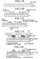
- FIGS. 11A-11E show steps of forming bumps on a wafer in batch in combination of Ni electroless plating and solder paste printing methods in order to reduce the cost of manufacture.
- FIG. 11A depicts a silicon substrate (wafer) having an SiO 2 film formed thereon
- FIG. 11B depicts an enlarged part of a chip portion including its electrodes.
- numeral 51 depicts an Si substrate (wafer)
- 55 depicts an Al electrode pad
- an Ni electroless plating layer (UBM: under bump metal) is formed selectively by the Ni electroless plating method.
- This Ni electroless plating layer serving as a UBM for supporting electric connection between the Al electrode pad 55 and the solder bump can be formed easily by the steps of pretreating the Al electrode pad 55 with a phosphoric acid etching solution, substitution-precipitating Zn by a Zn processing, and dip-coating in a Ni-P plating vessel.
- FIG. 11D shows a state in which a solder paste 59 is transferred onto the Ni electroless plating layer (UBM) through a metal screen mask 52 by a printing method.
- FIG. 11E shows a state in which the solder paste 59 is fused by a wet back method (hot fusing) to form a solder bump 62.
- the solder bump 62 can be formed easily by using the Ni electroless plating method and the solder paste screen printing method, or the like.
- the CSP which is an approach to a high density packaging of LSIs by minimizing respective chips thereof is comprised of several common circuit blocks as viewed from the standpoint of a digital device circuit block diagram, and there is emerging such a process to provide these common circuit blocks in a multi package or in a MCM (multi chip module).
- Provision of SRAM (static RAM), flash memory and a microcomputer in one chip package in a digital portable telephone is one example thereof.
- This MCM technology is expected to show a significant advantage also in a one-chip system LSI of a recent development. Namely, when integrating memory, logic and analog LSIs on one chip, different LSI fabrication processes must be handled in a same wafer processing step, thereby substantially increasing the number of masks and processing steps, and its TAT (turnaround time) for development being prolonged. Also, a low yield in production resulting from the increased steps of processing is a serious problem which cannot be ignored.
- FIGS. 12A and 12B show a wire-bonding method whereby each chip 62 mounted on a circuit substrate 60 is electrically connected using a wire 61 therebetween.
- FIGS. 13A-13C show a flip chip method whereby each chip 64 is connected to an electrode 63 on a circuit substrate 60 in a state of facedown.
- the flip chip method indicated in FIGS. 13A-13C is considered to be advantageous.
- the flip chip method is considered to take over.
- FIG. 13C shows an example which ensures a lower electric resistance connection to the substrate 60 by means of an intercalation bonding via a solder bump 65.
- the Au stud bump 24 indicated in FIG. 9 is formed by a method of forming a bump per chip.
- This method of forming a bump per chip is widely used as a simple bump forming method using existing facilities, however, there is a problem that as the number of termination pins increases, the cost of forming bumps will increase accordingly.
- the Au stud bump 24 in FIG. 9 is not suitable for use as this area pad in consideration of a bonding load and a susceptibility to damage. Still further, there is such a problem that a packaging of Au stud bump chips is done by press bonding of a piece by piece basis, and has a difficulty of mounting on both surfaces.
- the wafer batch solder bump forming method is advantageous in terms of packaging because it can be applied to the provision of the area pad, and enables a batch reflow or a double side mounting.
- it has a disadvantage when applying to the processing of a leading-edge wafer which normally has a low yield of production because a cost of production per non-defective chip will substantially increase.
- FIG. 14 which indicates a semiconductor wafer 53 fabricated by a conventional wafer batch processing, nevertheless a high yield of production is required for the leading-edge LSIs, the number of defective chips 20 partitioned by a scribe line 21 and marked with "x" is actually greater than the number of non-defective chips 3 marked with "o".
- the wafer batch bump forming method which has a high yield is advantageous for use in such a case where the number of terminals accommodated within a single wafer is large (for example, 50000 terminals/wafer), or for forming low damage bumps applicable to the area pad.
- the Au stud bump is advantageous for use in a bump treatment per chip in a case where the bare chips are purchased by lot, or for a simple bump treatment.
- a method of forming a wiring layer for interconnection between devices whereby a plurality of semiconductor chips are firmly bonded on a silicon wafer, embedded into a resin formed on a substrate made of alumina or the like under pressure, then peeled off so as to provide a flat wafer surface and form the wiring layer for interconnection between the devices on this flat wafer surface by photolithography.
- the present invention is contemplated to solve the above-mentioned problems associated with the conventional art, and to provide a chip-like electronic component such as a semiconductor chip which is comprised of leading-edge LSIs or bare chips even if they are purchased from outside, and can be mass-produced at a high yield, low cost and high reliability.
- the present invention is directed to chip-like electronic components such as semiconductor chips, wherein each of them has at least its electrodes formed exclusively on one surface thereof, all the rest of its surfaces without the electrodes are covered continuously with a protective substance and a pseudo wafer, which is comprised of a plurality and/or a plurality of different types chip-like electronic components bonded spaced apart from each other by the protective substance which is coated continuously therebetween and on their bottom surfaces.
- a method of manufacturing of the pseudo wafer is provided, which is comprised of the steps of: pasting an adhesive material on a substrate, retaining an adhesive strength prior to its processing and losing the adhesive strength post its processing; fixing a plurality and/or a plurality of different types of semiconductor chips on this adhesive material with their surfaces having electrodes facing downward; coating a protective material on a whole portion of the rest of the surfaces of the plurality and/or the plurality of different types of semiconductor chips including interspatial gaps therebetween; applying a predetermined processing to the adhesive material so as to lower the adhesive strength thereof; and peeling off the pseudo wafer having these semiconductor chips fixed thereon.
- a method of manufacturing of a chip-like electronic component is provided, which is comprised of the step of cutting off the protective material between respective semiconductor chips of the plurality and/or the plurality of different types of semiconductor chips on the wafer so as to separate and provide a discrete semiconductor chip or a chip-like electronic component.
- the portions of the chip-like electronic component such as the semiconductor chip or the like are protected continuously with a protective material, the chip is ensured to be protected in its post chip handling, thereby facilitating its handling and enabling an excellent package reliability to be obtained.
- the sidewall and the bottom surface of the chip are coated with the protective material such as a passivation film, an Ni electroless plating process can be applied as well.
- the protective material such as a passivation film
- an Ni electroless plating process can be applied as well.
- wafers of in-house product but also bare chips purchased from the other manufacturers are allowed to be subjected to the solder bump treatment likewise and easily.
- it is becoming a rare case that all of a plurality of different types of LSI chips to be packaged in an MCM are supplied from a same semiconductor manufacturer because of an increasing burden for investing on several leading edge semiconductor production lines simultaneously.
- the substrate described above can be used in repetition advantageously in terms of cost reduction of bump forming as well as environmentally.
- the above-mentioned protective material is an organic insulating resin or an inorganic insulating material.
- the semiconductor chip of the invention which is diced at the position of the protective material between respective semiconductor chips and mounted on a packaging substrate may be a single or a plurality of chips, or a plurality of different types of chips which are integrated by means of the protective material, wherein the above-mentioned electrodes are provided on the packaging surface thereof while the side wall and the bottom surface thereof are covered with the above-mentioned protective material, and preferably solder bumps are formed on the above-mentioned electrodes.
- a single semiconductor chip or an integrated semiconductor chip integrating a plurality of them or a plurality of different types of them to be mounted on a packaging substrate are obtained according to the invention by the method, comprising the steps of: pasting an adhesive sheet on a flat surface of a transparent substrate or the like; fixing a plurality of non-defective (conforming) semiconductor chips or a plurality of different types of them on this adhesive sheet, with the surfaces thereof having the electrodes facing down; uniformly coating the semiconductor chips from their bottom surfaces with the protective material which is the organic insulating resin or inorganic insulating material and subsequently hardening the same; then irradiating with ultraviolet rays from the bottom of the transparent substrate opposite to its surface on which the semiconductor chips are fixed, or applying a chemical solution or heating so as to weaken the adhesive strength of the above-mentioned adhesive sheet; peeling off from the substrate a pseudo wafer having the plurality of semiconductor chips and/or the plurality of different types of them bonded thereon with the protective material; thereby
- non-defective semiconductor chips or chip-like electronic components may be selected in such a manner that solely and only the semiconductor chips which are judged to be non-defective by characteristics measurements are allowed to be bonded on the above-mentioned substrate, or that they are subjected to the characteristics measurements in a state as bonded with the above-mentioned protective material and then only the non-defective semiconductor chips or chip-like electronic components are selected.
- FIG. 3 shows an example of intermediate wafers having only non-defective semiconductor bare chips 3 (or LSI chips) that are diced from the semiconductor wafer 53 indicated in FIG. 14, verified to be conforming to its specification in an open/shorted or DC voltage measurements, then arranged at an equidistance from each other and pasted on a circular quartz substrate 1 via an adhesive sheet 2 made of acrylic or the like.
- FIG. 4 shows another example thereof wherein a large-sized square glass substrate 19 is used instead of the circular quartz substrate 1 in order to allow for a greater number of non-defective chips 3 to be pasted on a relatively limited area via the adhesive sheet 2, thereby ensuring an improved cost merit to be attained in the subsequent processing.
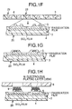
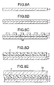
- FIG. 1A shows a quartz substrate 1 serving as a temporary support substrate.
- a heat process to be applied to this substrate is below 400°C, a less costly glass substrate may be used. Further, this quartz substrate 1 can be used in repetition.
- an adhesive sheet 2 made of such as acrylic which is used in a normal dicing and loses its adhesive strength when irradiated with ultraviolet rays is pasted on the quartz substrate 1.
- a plurality of non-defective bare chips 3 verified to be conforming as described above are arrayed and pasted on the adhesive sheet 2 with their chip surfaces (device surfaces) 28 facing down.
- these non-defective bare chips 3 may be selected from a dicing sheet (not shown) which was subjected to dicing in a wafer process and in an extended state, or may be transferred from a chip tray. What is important and to be noted here is that notwithstanding whether they are manufactured in-house or by other manufacturers, totally and only the non-defective bare chips 3 are allowed to be rearranged on the substrate 1.
- an organic insulating resin such as an acrylic resin 4 is coated uniformly on the chip 3 and a gap therebetween. This coating can be attained easily by a spin coating or printing methods.
- a pseudo wafer 29 comprising a plurality of non-defective bare chips 3 which are bonded continuously on their side walls and bottom surfaces is peeled off from the quartz substrate 1 at an adhesive surface 30.
- the pseudo wafer 29 is turned over so as to cause a non-defective bare chip's surface (device surface) 28 to face upward.
- the pseudo wafer 29 as partially enlarged in this figure has an Al electrode pad 5 and a passivation film formed on the silicon substrate via an SiO 2 film.
- FIGS. 1G-1I shows an Ni electroless plating process to provide a UBM
- FIG. 1H shows a print/transfer of a solder paste 9 using a print mask 8
- FIG. 1I shows a state of a solder bump 12 formed by a wet back method.
- an Ni electroless plating layer (UBM) is formed selectively by the Ni electroless plating method.
- This Ni electroless plating layer (UBM) is easily formed by the steps of: pretreating the upper surface of the Al electrode pad 5 with a phosphoric acid etching solution; then precipitating Zn by a zinc substitution process; and dipping in an Ni-P plating vessel.
- This Ni electroless plating layer functions as a UBM (under bump metal) which facilitates electric connection between the Al electrode pad 5 and the solder bump.
- FIG. 1H shows a state of a solder paste 9 which was transferred via the print mask 8 onto the Ni electroless plated layer (UBM) by the printing method.
- FIG. 1I shows a state in which the solder paste 9 is fused by the wet back method to form the solder bump 12.
- the solder bump 12 can be formed easily using the Ni electroless plating method and the solder paste screen printing method or the like, without need of using a photo process.
- step of FIG. 1I by carrying out measurements of electrical characteristics of the non-defective chips by a probe inspection and/or a burn-in processing, a more precise selection only of the non-defective bare chips 3 which passed prior selection before the step of FIG. 1C will be ensured.
- FIG. 1J shows a step of dicing the pseudo wafer 29 along a scribe line 33 with a blade 32 (or a laser beam) into discrete pieces of a non-defective chip component 26 which is comprised of the chip 3 which is protected and enforced by the resin 4.
- the non-defective chip component 26 diced into a discrete piece is mounted on a package substrate 27 which is provided with an electrode 14 which is surrounded by a solder resist 15 on a wiring substrate 16, and covered with a solder paste 13.
- the above description has been made by way of example of the flip chip packaging technique for packaging semiconductor chips, however, it is not limited thereto, and may be applied to an interconnection solder bump forming technique in a high density flip chip packaging and a method of fabrication thereof, wherein the non-defective bare chips 3 are arrayed at an equidistance and pasted on the quartz substrate 1 with their surfaces (device surface) 28 facing downward, then the resin 4 is coated uniformly on their bottom surfaces and therebetween thereby securing the non-defective chips 3 to be held firmly to each other.
- This bump chip of the invention can be used not only in compact, lightweight and portable electronic devices, but also in any other types of electronic devices.
- FIG. 2 shows a modified type of the bump forming method in which a metal ball (solder ball) 17 is used in place of the above-mentioned solder paste 9.
- a passivation film which covers the Al electrode pad 5 formed on the pseudo wafer is perforated at a position where a bump electrode is to be formed, and a Ni electroless plating layer (UBM) is formed therein.
- UBM Ni electroless plating layer
- a flux 18 is coated on this Ni electroless plated layer (UBM) by a printing method or the like.
- a material suitable for this flux 18 preferably has a high adhesive strength so as to facilitate a transfer of a metal ball 17, and a quantity of this coating is sufficient if the metal ball 17 is retained.
- the method for coating the flux 18 is not limited to the printing method, however, in practice, the printing method is preferable. It is because that in comparison with the other methods, this method is advantageous in that it can coat the flux 18 in a preferred pattern in a simple and efficient operation.
- the metal ball 17 which is mounted on the flux 18 is subjected to a reflow (fusing) process, and then the flux 18 is cleaned. Thereby, the metal ball 17 is ensured to attach to the Ni electroless plating layer (UBM) very strongly, thereby completing the process of forming bump electrodes.
- UBM Ni electroless plating layer
- the non-defective semiconductor chips diced from the wafer are rearranged and pasted on the substrate at the equidistance, then after coating with the resin, the pseudo wafer as if having totally and only the non-defective semiconductor chips is obtained. Therefore, the wafer batch processing for forming solder bumps on the plurality of the non-defective chips becomes possible, thereby enabling a chip having flip chip solder bumps to be formed at a low cost. Further, not only the wafers of the in-house product but also bare chips purchased from the other manufacturers can be processed alike to form solder bumps thereon easily according to the invention.
- the merit and the advantage of the low cost bump processing based on the wafer batch processing method of the invention can be utilized in processing of the leading-edge LSIs or bare chips purchased from the other manufacturer, thereby providing a novel bump forming method widely applicable.
- the dicing is carried out easily without damaging the cutter blade and minimizing adverse effects (strain, flash, crack and the like damages) on the body of the semiconductor chips.
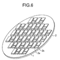
- FIGS. 5-7 show a second embodiment of the present invention for obtaining chip-like electronic components each packaged in an MCM (multi chip module) comprising a plurality of different types of non-defective chips.
- MCM multi chip module
- FIGS 5A-5J correspond respectively to FIGS. 1A-1J of the first embodiment described hereinabove, wherein the same components with the same reference numerals are omitted of their explanations, and the process of FIG. 1K is executed in the same manner also in this second embodiment.
- the semiconductor chips 3 in the step of FIG. 5C, as the semiconductor chips 3, a plurality of different types of semiconductor chips 3a and 3b are pasted on the quartz substrate 1, then they are treated in the same manner as described in the first embodiment. However, as shown in FIG. 5J, the plurality of different types of semiconductor chips 3a and 3b are scribed into various patterns of combinations thereof, and diced into non-defective chip-like components 26 for providing MCMs.
- FIG. 6 shows an example of equidistantly re-arranged plurality of different types of semiconductor chips 3a and 3b (or LSI chips) which are diced from the semiconductor wafer, verified to be conforming (non-defective) in an open/short-circuited or DC voltage measurements, and pasted on a circular quartz substrate 1 via the adhesive sheet 2 made of acrylic or the like.
- FIG. 6 shows an example of equidistantly re-arranged plurality of different types of semiconductor chips 3a and 3b (or LSI chips) which are diced from the semiconductor wafer, verified to be conforming (non-defective) in an open/short-circuited or DC voltage measurements, and pasted on a circular quartz substrate 1 via the adhesive sheet 2 made of acrylic or the like.
- FIG. 7 shows another example of the above in which a greater number of non-defective chips 3 are pasted via the adhesive sheet 2 on a larger-sized square glass substrate 19 which is used in place of the circular quartz substrate 1 so as to allow for the greater number of non-defective chips to be pasted on a limited area, thereby allowing for an increased cost merit to be attained in the subsequent processing.
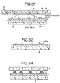
- a third embodiment of the present invention is described, in which a SOG (spin on glass) film 4' which consists of an inorganic insulating material such as SiO x is used instead of the resin 4 used in the first embodiment for embedding the non-defective chips 3, then after heating or the like, a pseudo wafer 29 for use in fabrication of MCMs is peeled off.
- SOG spin on glass
- FIG. 8A depicts a substrate 1' which serves as a temporary support substrate.
- the substrate 1' used here is not limited to the above-mentioned quartz substrate or the glass substrate, but other non-transparent substrates such as Si or a metal plate may be used alike.
- an adhesive sheet 2' made of, for example, acrylic, which is used in normal dicing and has a property to lose its adhesive strength when subjected to a chemical solution or heating is pasted on the substrate 1'.
- a plurality of semiconductor bare chips 3 which are confirmed to be non-defective and conforming as described hereinabove are arrayed and pasted on the adhesive sheet 2' with their chip surfaces (device surfaces) 28 facing downward.
- the plurality of non-defective bare chips 3 used here may be selected directly from an extended dicing sheet (not shown) used in dicing in the normal wafer process as shown in FIG. 14, or may be transferred from a chip tray. What is important and should be note here is that notwithstanding whether they are in-house products or those purchased from outside, totally and only the non-defective or conforming bare chips 3 are allowed to be rearranged on the substrate 1.
- this non-defective chip 3 is specially designed suitable for a multi chip module packaging. Further, preferably, the same has a small pad (approximately ⁇ 20 nm ⁇ ) for inter-chip wiring, and a test pad for testing each chip.
- the insulating material 4' such as SOG or the like is coated from above the chips 3 thereby embedding the chips 3.
- the adhesive strength of the adhesive sheet 2' is weakened by applying a chemical solution or heating so as to allow for both of the Si wafer 70 and the embedded chips 3 firmly retained by the adhesive strength of the insulating material 4' to be removed from the substrate 1' as depicted in FIG. 8F.
- the packaging process may proceed in the same flow of steps as indicated in FIGS. 1I-1K.
- the substrate on which the non-defective bare chips are to be pasted may be comprised of any other materials instead of the quartz or glass if it has the same function and strength. Further, the shape and thickness of its substrate can be modified at discretion. Also, various types of acrylic or other materials may be used as the adhesive sheets 2 and 2' if it has the same function. Materials for the resin 4 and insulating material 4' may be selected from the group consisting of the similar materials. In addition, the distance between the plurality of non-defective bare chips 3 at which they are arrayed may be selected at discrete if it is equidistant.
- the substrate such as the quartz substrate 1 described heretofore can be used repeatedly thereby providing substantial advantages in cost merits and environmental protection.
- the object of application of the invention is not limited to the semiconductor chips described hereinabove, but is also applicable to any other chip-like electronic components which involve the process of dicing into discrete chips during its fabrication.
Landscapes
- Dicing (AREA)
- Encapsulation Of And Coatings For Semiconductor Or Solid State Devices (AREA)
- Container, Conveyance, Adherence, Positioning, Of Wafer (AREA)
Applications Claiming Priority (2)
| Application Number | Priority Date | Filing Date | Title |
|---|---|---|---|
| JP2000122112A JP4403631B2 (ja) | 2000-04-24 | 2000-04-24 | チップ状電子部品の製造方法、並びにその製造に用いる擬似ウエーハの製造方法 |
| JP2000122112 | 2000-04-24 |
Publications (3)
| Publication Number | Publication Date |
|---|---|
| EP1150552A2 true EP1150552A2 (fr) | 2001-10-31 |
| EP1150552A3 EP1150552A3 (fr) | 2003-05-28 |
| EP1150552B1 EP1150552B1 (fr) | 2005-04-13 |
Family
ID=18632631
Family Applications (1)
| Application Number | Title | Priority Date | Filing Date |
|---|---|---|---|
| EP01109863A Expired - Lifetime EP1150552B1 (fr) | 2000-04-24 | 2001-04-23 | Composant électronique en forme de pastille, son procédé de fabrication, une pseudo plaquette et son procédé de fabrication |
Country Status (6)
| Country | Link |
|---|---|
| US (2) | US20020011655A1 (fr) |
| EP (1) | EP1150552B1 (fr) |
| JP (1) | JP4403631B2 (fr) |
| KR (1) | KR100818534B1 (fr) |
| DE (1) | DE60109983T2 (fr) |
| TW (1) | TWI239056B (fr) |
Cited By (9)
| Publication number | Priority date | Publication date | Assignee | Title |
|---|---|---|---|---|
| DE102004027489A1 (de) * | 2004-06-04 | 2005-12-29 | Infineon Technologies Ag | Verfahren zum Anordnen von Chips eines ersten Substrats auf einem zweiten Substrat |
| DE102005013500A1 (de) * | 2005-03-23 | 2006-10-05 | Infineon Technologies Ag | Halbleiteranordnung und Verfahren zum Herstellen einer Halbleiteranordnung |
| WO2010070103A1 (fr) * | 2008-12-19 | 2010-06-24 | 3D Plus | Procede de fabrication collective de modules electroniques pour montage en surface |
| US7824962B2 (en) | 2008-01-29 | 2010-11-02 | Infineon Technologies Ag | Method of integrated circuit fabrication |
| US8629001B2 (en) | 2009-07-13 | 2014-01-14 | Kabushiki Kaisha Toshiba | Semiconductor device and method of manufacturing semiconductor device |
| CN103531697A (zh) * | 2012-06-29 | 2014-01-22 | 日东电工株式会社 | 覆有密封层的半导体元件、其制造方法及半导体装置 |
| EP2750211A3 (fr) * | 2012-12-28 | 2016-01-20 | Nitto Denko Corporation | Élément semi-conducteur optique recouvert d'une couche d'encapsulation, son procédé de production et dispositif semi-conducteur |
| EP2680330A3 (fr) * | 2012-06-29 | 2016-01-20 | Nitto Denko Corporation | Élément semi-conducteur recouvert d'une couche d'encapsulation, son procédé de production et dispositif semi-conducteur |
| US11069654B2 (en) | 2016-06-01 | 2021-07-20 | Sony Corporation | Metal frame, dummy wafer, semiconductor device, electronic device, and method of manufacturing semiconductor device |
Families Citing this family (75)
| Publication number | Priority date | Publication date | Assignee | Title |
|---|---|---|---|---|
| KR100421774B1 (ko) | 1999-12-16 | 2004-03-10 | 앰코 테크놀로지 코리아 주식회사 | 반도체패키지 및 그 제조 방법 |
| JP2001313350A (ja) * | 2000-04-28 | 2001-11-09 | Sony Corp | チップ状電子部品及びその製造方法、並びにその製造に用いる疑似ウエーハ及びその製造方法 |
| KR20020091327A (ko) * | 2001-05-31 | 2002-12-06 | 삼성전자 주식회사 | 측면 몸체부가 형성되어 있는 웨이퍼 레벨 패키지 및 그제조 방법 |
| DE10145382A1 (de) * | 2001-09-14 | 2003-01-09 | Infineon Technologies Ag | Verfahren zur Herstellung eines elektronischen Bauelements, insbesondere eines Chips |
| KR100455387B1 (ko) | 2002-05-17 | 2004-11-06 | 삼성전자주식회사 | 반도체 칩의 범프의 제조방법과 이를 이용한 cog 패키지 |
| US7183582B2 (en) | 2002-05-29 | 2007-02-27 | Seiko Epson Coporation | Electro-optical device and method of manufacturing the same, element driving device and method of manufacturing the same, element substrate, and electronic apparatus |
| JP3942500B2 (ja) | 2002-07-02 | 2007-07-11 | Necエレクトロニクス株式会社 | 半導体装置の製造方法 |
| JP3618331B2 (ja) | 2002-11-08 | 2005-02-09 | 沖電気工業株式会社 | 半導体装置及びその製造方法 |
| JP3618330B2 (ja) | 2002-11-08 | 2005-02-09 | 沖電気工業株式会社 | 半導体装置及びその製造方法 |
| JP3617647B2 (ja) | 2002-11-08 | 2005-02-09 | 沖電気工業株式会社 | 半導体装置及びその製造方法 |
| JP4056360B2 (ja) | 2002-11-08 | 2008-03-05 | 沖電気工業株式会社 | 半導体装置及びその製造方法 |
| JP3844467B2 (ja) | 2003-01-08 | 2006-11-15 | 沖電気工業株式会社 | 半導体装置及びその製造方法 |
| US7915085B2 (en) | 2003-09-18 | 2011-03-29 | Cree, Inc. | Molded chip fabrication method |
| US7326592B2 (en) * | 2005-04-04 | 2008-02-05 | Infineon Technologies Ag | Stacked die package |
| KR100688560B1 (ko) | 2005-07-22 | 2007-03-02 | 삼성전자주식회사 | 웨이퍼 레벨 칩 스케일 패키지 및 그 제조 방법 |
| JP4837971B2 (ja) * | 2005-10-07 | 2011-12-14 | ルネサスエレクトロニクス株式会社 | 半導体装置の製造方法 |
| US7361531B2 (en) | 2005-11-01 | 2008-04-22 | Allegro Microsystems, Inc. | Methods and apparatus for Flip-Chip-On-Lead semiconductor package |
| US7382038B2 (en) * | 2006-03-22 | 2008-06-03 | United Microelectronics Corp. | Semiconductor wafer and method for making the same |
| US9159888B2 (en) | 2007-01-22 | 2015-10-13 | Cree, Inc. | Wafer level phosphor coating method and devices fabricated utilizing method |
| US9024349B2 (en) | 2007-01-22 | 2015-05-05 | Cree, Inc. | Wafer level phosphor coating method and devices fabricated utilizing method |
| US7888850B2 (en) * | 2007-01-30 | 2011-02-15 | Nihon Dempa Kogyo Co., Ltd. | Tuning-fork type piezoelectric unit |
| US20090014852A1 (en) * | 2007-07-11 | 2009-01-15 | Hsin-Hui Lee | Flip-Chip Packaging with Stud Bumps |
| US9041285B2 (en) | 2007-12-14 | 2015-05-26 | Cree, Inc. | Phosphor distribution in LED lamps using centrifugal force |
| US8878219B2 (en) | 2008-01-11 | 2014-11-04 | Cree, Inc. | Flip-chip phosphor coating method and devices fabricated utilizing method |
| CN102077341B (zh) * | 2008-06-26 | 2014-04-23 | Nxp股份有限公司 | 封装半导体产品及其制造方法 |
| JP2010092931A (ja) * | 2008-10-03 | 2010-04-22 | Toshiba Corp | 半導体装置の製造方法及び半導体装置の製造装置 |
| US9691734B1 (en) | 2009-12-07 | 2017-06-27 | Amkor Technology, Inc. | Method of forming a plurality of electronic component packages |
| EP2515329A1 (fr) * | 2009-12-14 | 2012-10-24 | Sumitomo Bakelite Co., Ltd. | Procédé de production de dispositif électronique, dispositif électronique, procédé de production de boîtier de dispositif électronique et boîtier de dispositif électronique |
| JP5137937B2 (ja) | 2009-12-16 | 2013-02-06 | 日東電工株式会社 | 半導体装置製造用耐熱性粘着シート、該シートに用いる粘着剤、及び該シートを用いた半導体装置の製造方法 |
| JP5144634B2 (ja) | 2009-12-22 | 2013-02-13 | 日東電工株式会社 | 基板レス半導体パッケージ製造用耐熱性粘着シート、及びその粘着シートを用いる基板レス半導体パッケージ製造方法 |
| US8294276B1 (en) | 2010-05-27 | 2012-10-23 | Amkor Technology, Inc. | Semiconductor device and fabricating method thereof |
| US10546846B2 (en) | 2010-07-23 | 2020-01-28 | Cree, Inc. | Light transmission control for masking appearance of solid state light sources |
| JP2012114297A (ja) * | 2010-11-25 | 2012-06-14 | Sumitomo Bakelite Co Ltd | 電子装置の製造方法、電子装置、電子装置パッケージの製造方法および電子装置パッケージ |
| JP5635378B2 (ja) | 2010-11-30 | 2014-12-03 | 日東電工株式会社 | 半導体ウエハ搬送方法および半導体ウエハ搬送装置 |
| US9166126B2 (en) | 2011-01-31 | 2015-10-20 | Cree, Inc. | Conformally coated light emitting devices and methods for providing the same |
| JP5717502B2 (ja) * | 2011-03-30 | 2015-05-13 | 信越ポリマー株式会社 | 半導体チップ用保持具及びその使用方法 |
| WO2012152307A1 (fr) * | 2011-05-06 | 2012-11-15 | Osram Opto Semiconductors Gmbh | Ensemble support de composants comprenant une structure de tranchées séparant les zones de support de composants et procédé de fabrication d'une pluralité de zones de support de composants |
| US20140044957A1 (en) | 2011-07-15 | 2014-02-13 | Nitto Denko Corporation | Production method for electronic component and pressure-sensitive adhesive sheet to be used in the production method |
| JP5959216B2 (ja) | 2012-02-06 | 2016-08-02 | 日東電工株式会社 | 基板搬送方法および基板搬送装置 |
| JP2013168417A (ja) | 2012-02-14 | 2013-08-29 | Nitto Denko Corp | 基板搬送方法および基板搬送装置 |
| JP5903920B2 (ja) * | 2012-02-16 | 2016-04-13 | 富士通株式会社 | 半導体装置の製造方法及び電子装置の製造方法 |
| JP5810957B2 (ja) | 2012-02-17 | 2015-11-11 | 富士通株式会社 | 半導体装置の製造方法及び電子装置の製造方法 |
| JP5810958B2 (ja) | 2012-02-17 | 2015-11-11 | 富士通株式会社 | 半導体装置の製造方法及び電子装置の製造方法 |
| US20130234344A1 (en) * | 2012-03-06 | 2013-09-12 | Triquint Semiconductor, Inc. | Flip-chip packaging techniques and configurations |
| JP5728423B2 (ja) | 2012-03-08 | 2015-06-03 | 株式会社東芝 | 半導体装置の製造方法、半導体集積装置及びその製造方法 |
| EP2639278A1 (fr) | 2012-03-13 | 2013-09-18 | Nitto Denko Corporation | Ruban adhésif sensible à la pression résistant à la chaleur pour la fabrication d'un dispositif semi-conducteur et procédé de fabrication de dispositif semi-conducteur utilisant le ruban |
| EP2639277A1 (fr) | 2012-03-13 | 2013-09-18 | Nitto Denko Corporation | Ruban adhésif sensible à la pression résistant à la chaleur pour la fabrication d'un dispositif semi-conducteur et procédé de fabrication de dispositif semi-conducteur utilisant le ruban |
| JP6154995B2 (ja) * | 2012-06-20 | 2017-06-28 | 新光電気工業株式会社 | 半導体装置及び配線基板、並びにそれらの製造方法 |
| US20140009060A1 (en) | 2012-06-29 | 2014-01-09 | Nitto Denko Corporation | Phosphor layer-covered led, producing method thereof, and led device |
| US20140001948A1 (en) | 2012-06-29 | 2014-01-02 | Nitto Denko Corporation | Reflecting layer-phosphor layer-covered led, producing method thereof, led device, and producing method thereof |
| JP6055259B2 (ja) | 2012-10-03 | 2016-12-27 | 日東電工株式会社 | 封止シート被覆半導体素子、その製造方法、半導体装置およびその製造方法 |
| JP2014090157A (ja) | 2012-10-03 | 2014-05-15 | Nitto Denko Corp | 封止シート被覆半導体素子、その製造方法、半導体装置およびその製造方法 |
| US8523046B1 (en) * | 2012-10-18 | 2013-09-03 | International Business Machines Corporation | Forming an array of metal balls or shapes on a substrate |
| JP5768864B2 (ja) * | 2013-11-20 | 2015-08-26 | 株式会社デンソー | 電子装置の製造方法 |
| US9202793B1 (en) * | 2013-12-26 | 2015-12-01 | Stats Chippac Ltd. | Integrated circuit packaging system with under bump metallization and method of manufacture thereof |
| JP6378501B2 (ja) | 2014-03-05 | 2018-08-22 | 日東電工株式会社 | 粘着シート |
| US9478453B2 (en) * | 2014-09-17 | 2016-10-25 | International Business Machines Corporation | Sacrificial carrier dicing of semiconductor wafers |
| JP6503286B2 (ja) * | 2015-12-24 | 2019-04-17 | ルネサスエレクトロニクス株式会社 | 半導体装置の製造方法および半導体ウェハ |
| GB2546740A (en) | 2016-01-26 | 2017-08-02 | Worldpay Ltd | Electronic payment system and method |
| DE102017215177B4 (de) * | 2016-09-02 | 2024-10-10 | Idex Biometrics Asa | Verfahren zur Herstellung eines Abdeckungselements geeignet für einen Fingerprint Sensor |
| US9892989B1 (en) * | 2016-12-08 | 2018-02-13 | Nxp B.V. | Wafer-level chip scale package with side protection |
| US11581197B2 (en) | 2017-05-10 | 2023-02-14 | Mitsui Chemicals, Inc. | Method for producing semiconductor device and intermediate for semiconductor device |
| CN109216201A (zh) * | 2017-07-07 | 2019-01-15 | 恒劲科技股份有限公司 | 以大板面工艺制作晶粒凸块结构的方法 |
| WO2020021666A1 (fr) * | 2018-07-25 | 2020-01-30 | 株式会社Fuji | Dispositif de détermination et appareil d'installation de puce équipé de celui-ci |
| US10643957B2 (en) | 2018-08-27 | 2020-05-05 | Nxp B.V. | Conformal dummy die |
| JPWO2022123931A1 (fr) | 2020-12-07 | 2022-06-16 | ||
| DE112021005267T5 (de) | 2020-12-07 | 2023-07-20 | Nitto Denko Corporation | Haftklebstofflage |
| KR102900489B1 (ko) | 2021-01-15 | 2025-12-16 | 닛토덴코 가부시키가이샤 | 점착 시트 |
| JP7568825B2 (ja) | 2021-03-05 | 2024-10-16 | 日東電工株式会社 | 粘着シート |
| CN117642475A (zh) | 2021-07-13 | 2024-03-01 | 日东电工株式会社 | 粘合片 |
| CN117751171A (zh) | 2021-07-13 | 2024-03-22 | 日东电工株式会社 | 粘合片 |
| JPWO2023286619A1 (fr) | 2021-07-13 | 2023-01-19 | ||
| CN116031193A (zh) * | 2021-10-25 | 2023-04-28 | 升新高科技(南京)有限公司 | 一种方形晶粒的凸块制备方法及圆形晶圆片结构 |
| JP2024090083A (ja) | 2022-12-22 | 2024-07-04 | 日東電工株式会社 | 粘着シート |
| JP2024102584A (ja) | 2023-01-19 | 2024-07-31 | 日東電工株式会社 | 粘着シート |
Family Cites Families (63)
| Publication number | Priority date | Publication date | Assignee | Title |
|---|---|---|---|---|
| US3706129A (en) * | 1970-07-27 | 1972-12-19 | Gen Electric | Integrated semiconductor rectifiers and processes for their fabrication |
| CA1003122A (en) * | 1973-04-30 | 1977-01-04 | Lewis H. Trevail | Method of making multiple isolated semiconductor chip units |
| US4878099A (en) * | 1982-12-08 | 1989-10-31 | International Rectifier Corporation | Metallizing system for semiconductor wafers |
| FR2572849B1 (fr) * | 1984-11-06 | 1987-06-19 | Thomson Csf | Module monolithique haute densite comportant des composants electroniques interconnectes et son procede de fabrication |
| JPH074995B2 (ja) | 1986-05-20 | 1995-01-25 | 株式会社東芝 | Icカ−ド及びその製造方法 |
| JP2579937B2 (ja) * | 1987-04-15 | 1997-02-12 | 株式会社東芝 | 電子回路装置およびその製造方法 |
| US5032543A (en) * | 1988-06-17 | 1991-07-16 | Massachusetts Institute Of Technology | Coplanar packaging techniques for multichip circuits |
| JPH0353546A (ja) * | 1989-07-21 | 1991-03-07 | Mitsubishi Electric Corp | 半導体装置の製造方法およびその製造装置 |
| JP3128878B2 (ja) | 1991-08-23 | 2001-01-29 | ソニー株式会社 | 半導体装置 |
| JPH0590559A (ja) | 1991-09-27 | 1993-04-09 | Matsushita Electric Ind Co Ltd | 密着型イメージセンサ |
| GB2263195B (en) * | 1992-01-08 | 1996-03-20 | Murata Manufacturing Co | Component supply method |
| US5496775A (en) * | 1992-07-15 | 1996-03-05 | Micron Semiconductor, Inc. | Semiconductor device having ball-bonded pads |
| DK0660967T3 (da) * | 1992-09-14 | 2001-08-13 | Shellcase Ltd | Fremgangsmåde til fremstilling af integrerede kredsløbsanordninger |
| JPH06163808A (ja) | 1992-11-18 | 1994-06-10 | Hitachi Ltd | 半導体メモリおよびその応用システム |
| US5353498A (en) * | 1993-02-08 | 1994-10-11 | General Electric Company | Method for fabricating an integrated circuit module |
| US5796164A (en) | 1993-05-11 | 1998-08-18 | Micromodule Systems, Inc. | Packaging and interconnect system for integrated circuits |
| EP0668611A1 (fr) * | 1994-02-22 | 1995-08-23 | International Business Machines Corporation | Méthode pour recouvrir des puces semi-conductrices nues dans des boîtiers en plastique |
| US5567654A (en) | 1994-09-28 | 1996-10-22 | International Business Machines Corporation | Method and workpiece for connecting a thin layer to a monolithic electronic module's surface and associated module packaging |
| US5976955A (en) * | 1995-01-04 | 1999-11-02 | Micron Technology, Inc. | Packaging for bare dice employing EMR-sensitive adhesives |
| DE69635397T2 (de) * | 1995-03-24 | 2006-05-24 | Shinko Electric Industries Co., Ltd. | Halbleitervorrichtung mit Chipabmessungen und Herstellungsverfahren |
| US5600181A (en) | 1995-05-24 | 1997-02-04 | Lockheed Martin Corporation | Hermetically sealed high density multi-chip package |
| JP3018971B2 (ja) | 1995-12-18 | 2000-03-13 | 富士電機株式会社 | 半導体装置 |
| US6072236A (en) * | 1996-03-07 | 2000-06-06 | Micron Technology, Inc. | Micromachined chip scale package |
| JP3388674B2 (ja) * | 1996-04-19 | 2003-03-24 | リンテック株式会社 | エネルギー線硬化型感圧接着剤組成物およびその利用方法 |
| US5841193A (en) * | 1996-05-20 | 1998-11-24 | Epic Technologies, Inc. | Single chip modules, repairable multichip modules, and methods of fabrication thereof |
| US6407333B1 (en) | 1997-11-04 | 2002-06-18 | Texas Instruments Incorporated | Wafer level packaging |
| US6130116A (en) * | 1996-12-13 | 2000-10-10 | Tessera, Inc. | Method of encapsulating a microelectronic assembly utilizing a barrier |
| US5953588A (en) * | 1996-12-21 | 1999-09-14 | Irvine Sensors Corporation | Stackable layers containing encapsulated IC chips |
| US6117705A (en) * | 1997-04-18 | 2000-09-12 | Amkor Technology, Inc. | Method of making integrated circuit package having adhesive bead supporting planar lid above planar substrate |
| KR100253116B1 (ko) * | 1997-07-07 | 2000-04-15 | 윤덕용 | Le방법을 이용한 칩사이즈 패키지의 제조방법 |
| US5863813A (en) * | 1997-08-20 | 1999-01-26 | Micron Communications, Inc. | Method of processing semiconductive material wafers and method of forming flip chips and semiconductor chips |
| JP3526731B2 (ja) * | 1997-10-08 | 2004-05-17 | 沖電気工業株式会社 | 半導体装置およびその製造方法 |
| US5899705A (en) | 1997-11-20 | 1999-05-04 | Akram; Salman | Stacked leads-over chip multi-chip module |
| US5944199A (en) | 1997-11-25 | 1999-08-31 | Micron Technology, Inc. | Integrated circuit package support system |
| US5981310A (en) | 1998-01-22 | 1999-11-09 | International Business Machines Corporation | Multi-chip heat-sink cap assembly |
| US5933713A (en) * | 1998-04-06 | 1999-08-03 | Micron Technology, Inc. | Method of forming overmolded chip scale package and resulting product |
| US6133634A (en) * | 1998-08-05 | 2000-10-17 | Fairchild Semiconductor Corporation | High performance flip chip package |
| JP3516592B2 (ja) * | 1998-08-18 | 2004-04-05 | 沖電気工業株式会社 | 半導体装置およびその製造方法 |
| FR2788375B1 (fr) * | 1999-01-11 | 2003-07-18 | Gemplus Card Int | Procede de protection de puce de circuit integre |
| JP3556503B2 (ja) | 1999-01-20 | 2004-08-18 | 沖電気工業株式会社 | 樹脂封止型半導体装置の製造方法 |
| US6306680B1 (en) * | 1999-02-22 | 2001-10-23 | General Electric Company | Power overlay chip scale packages for discrete power devices |
| US6117704A (en) * | 1999-03-31 | 2000-09-12 | Irvine Sensors Corporation | Stackable layers containing encapsulated chips |
| US6338980B1 (en) * | 1999-08-13 | 2002-01-15 | Citizen Watch Co., Ltd. | Method for manufacturing chip-scale package and manufacturing IC chip |
| JP2001110828A (ja) | 1999-10-13 | 2001-04-20 | Sanyo Electric Co Ltd | 半導体装置の製造方法 |
| US6291884B1 (en) | 1999-11-09 | 2001-09-18 | Amkor Technology, Inc. | Chip-size semiconductor packages |
| US6271469B1 (en) * | 1999-11-12 | 2001-08-07 | Intel Corporation | Direct build-up layer on an encapsulated die package |
| US6242283B1 (en) | 1999-12-30 | 2001-06-05 | Siliconware Precision Industries Co., Ltd. | Wafer level packaging process of semiconductor |
| US6452265B1 (en) * | 2000-01-28 | 2002-09-17 | International Business Machines Corporation | Multi-chip module utilizing a nonconductive material surrounding the chips that has a similar coefficient of thermal expansion |
| US6348728B1 (en) | 2000-01-28 | 2002-02-19 | Fujitsu Limited | Semiconductor device having a plurality of semiconductor elements interconnected by a redistribution layer |
| JP3456462B2 (ja) * | 2000-02-28 | 2003-10-14 | 日本電気株式会社 | 半導体装置及びその製造方法 |
| US6344401B1 (en) * | 2000-03-09 | 2002-02-05 | Atmel Corporation | Method of forming a stacked-die integrated circuit chip package on a water level |
| US6603191B2 (en) * | 2000-05-18 | 2003-08-05 | Casio Computer Co., Ltd. | Semiconductor device and method of manufacturing the same |
| US6420212B1 (en) * | 2000-07-07 | 2002-07-16 | National Semiconductor Corporation | Method and apparatus to enclose dice |
| JP2002043251A (ja) * | 2000-07-25 | 2002-02-08 | Fujitsu Ltd | 半導体装置の製造方法及び半導体装置 |
| US6445591B1 (en) | 2000-08-10 | 2002-09-03 | Nortel Networks Limited | Multilayer circuit board |
| US6423570B1 (en) * | 2000-10-18 | 2002-07-23 | Intel Corporation | Method to protect an encapsulated die package during back grinding with a solder metallization layer and devices formed thereby |
| US6555906B2 (en) | 2000-12-15 | 2003-04-29 | Intel Corporation | Microelectronic package having a bumpless laminated interconnection layer |
| US6562663B2 (en) * | 2001-03-28 | 2003-05-13 | Motorola, Inc. | Microelectronic assembly with die support and method |
| JP2003007652A (ja) * | 2001-06-26 | 2003-01-10 | Mitsubishi Electric Corp | 半導体チップの製造方法 |
| US6541352B2 (en) * | 2001-07-27 | 2003-04-01 | Texas Instruments Incorporated | Semiconductor die with contoured bottom surface and method for making same |
| US6551863B2 (en) * | 2001-08-30 | 2003-04-22 | Micron Technology, Inc. | Flip chip dip coating encapsulant |
| JP2003273279A (ja) * | 2002-03-18 | 2003-09-26 | Mitsubishi Electric Corp | 半導体装置およびその製造方法 |
| US6964881B2 (en) * | 2002-08-27 | 2005-11-15 | Micron Technology, Inc. | Multi-chip wafer level system packages and methods of forming same |
-
2000
- 2000-04-24 JP JP2000122112A patent/JP4403631B2/ja not_active Expired - Lifetime
-
2001
- 2001-04-10 TW TW090108533A patent/TWI239056B/zh not_active IP Right Cessation
- 2001-04-23 DE DE60109983T patent/DE60109983T2/de not_active Expired - Lifetime
- 2001-04-23 EP EP01109863A patent/EP1150552B1/fr not_active Expired - Lifetime
- 2001-04-24 US US09/841,582 patent/US20020011655A1/en not_active Abandoned
- 2001-04-24 KR KR1020010022004A patent/KR100818534B1/ko not_active Expired - Fee Related
-
2002
- 2002-09-06 US US10/236,771 patent/US6936525B2/en not_active Expired - Lifetime
Cited By (16)
| Publication number | Priority date | Publication date | Assignee | Title |
|---|---|---|---|---|
| US7652493B2 (en) | 2004-06-04 | 2010-01-26 | Infineon Technologies Ag | Test arrangement having chips of a first substrate on a second substrate and chips of the second substrate on a third substrate |
| DE102004027489B4 (de) * | 2004-06-04 | 2017-03-02 | Infineon Technologies Ag | Verfahren zum Anordnen von Chips eines ersten Substrats auf einem zweiten Substrat |
| DE102004027489A1 (de) * | 2004-06-04 | 2005-12-29 | Infineon Technologies Ag | Verfahren zum Anordnen von Chips eines ersten Substrats auf einem zweiten Substrat |
| US7772039B2 (en) | 2004-06-04 | 2010-08-10 | Infineon Technologies Ag | Procedure for arranging chips of a first substrate on a second substrate |
| US7902683B2 (en) | 2005-03-23 | 2011-03-08 | Infineon Technologies Ag | Semiconductor arrangement and method for producing a semiconductor arrangement |
| DE102005013500A1 (de) * | 2005-03-23 | 2006-10-05 | Infineon Technologies Ag | Halbleiteranordnung und Verfahren zum Herstellen einer Halbleiteranordnung |
| US7824962B2 (en) | 2008-01-29 | 2010-11-02 | Infineon Technologies Ag | Method of integrated circuit fabrication |
| US8359740B2 (en) | 2008-12-19 | 2013-01-29 | 3D Plus | Process for the wafer-scale fabrication of electronic modules for surface mounting |
| FR2940521A1 (fr) * | 2008-12-19 | 2010-06-25 | 3D Plus | Procede de fabrication collective de modules electroniques pour montage en surface |
| WO2010070103A1 (fr) * | 2008-12-19 | 2010-06-24 | 3D Plus | Procede de fabrication collective de modules electroniques pour montage en surface |
| US8629001B2 (en) | 2009-07-13 | 2014-01-14 | Kabushiki Kaisha Toshiba | Semiconductor device and method of manufacturing semiconductor device |
| CN103531697A (zh) * | 2012-06-29 | 2014-01-22 | 日东电工株式会社 | 覆有密封层的半导体元件、其制造方法及半导体装置 |
| EP2680331A3 (fr) * | 2012-06-29 | 2016-01-20 | Nitto Denko Corporation | Élément semi-conducteur recouvert d'une couche d'encapsulation, son procédé de production et dispositif semi-conducteur |
| EP2680330A3 (fr) * | 2012-06-29 | 2016-01-20 | Nitto Denko Corporation | Élément semi-conducteur recouvert d'une couche d'encapsulation, son procédé de production et dispositif semi-conducteur |
| EP2750211A3 (fr) * | 2012-12-28 | 2016-01-20 | Nitto Denko Corporation | Élément semi-conducteur optique recouvert d'une couche d'encapsulation, son procédé de production et dispositif semi-conducteur |
| US11069654B2 (en) | 2016-06-01 | 2021-07-20 | Sony Corporation | Metal frame, dummy wafer, semiconductor device, electronic device, and method of manufacturing semiconductor device |
Also Published As
| Publication number | Publication date |
|---|---|
| EP1150552B1 (fr) | 2005-04-13 |
| JP2001308116A (ja) | 2001-11-02 |
| DE60109983D1 (de) | 2005-05-19 |
| TWI239056B (en) | 2005-09-01 |
| US20020011655A1 (en) | 2002-01-31 |
| DE60109983T2 (de) | 2006-02-23 |
| EP1150552A3 (fr) | 2003-05-28 |
| KR100818534B1 (ko) | 2008-04-02 |
| KR20010098833A (ko) | 2001-11-08 |
| US6936525B2 (en) | 2005-08-30 |
| US20030092252A1 (en) | 2003-05-15 |
| JP4403631B2 (ja) | 2010-01-27 |
Similar Documents
| Publication | Publication Date | Title |
|---|---|---|
| US6936525B2 (en) | Chip-like electronic components, a method of manufacturing the same, a pseudo wafer therefor and a method of manufacturing thereof | |
| US6841454B2 (en) | Chip-like electronic components, a method of manufacturing the same, a pseudo wafer therefor and a method of manufacturing thereof | |
| JP3701542B2 (ja) | 半導体装置およびその製造方法 | |
| US20090189279A1 (en) | Methods and systems for packaging integrated circuits | |
| JPH09199506A (ja) | 半導体素子のバンプ形成方法 | |
| TWI233188B (en) | Quad flat no-lead package structure and manufacturing method thereof | |
| US20090206480A1 (en) | Fabricating low cost solder bumps on integrated circuit wafers | |
| US20050140027A1 (en) | Method and device for manufacturing bonding pads for chip scale packaging | |
| JP2002093830A (ja) | チップ状電子部品の製造方法、及びその製造に用いる疑似ウェーハの製造方法 | |
| JP2002299546A (ja) | チップ状電子部品及びその製造方法、並びにその製造に用いる疑似ウエーハ及びその製造方法 | |
| JP2004103738A (ja) | 半導体装置及びその製造方法 | |
| JP2001338932A (ja) | 半導体装置及び半導体装置の製造方法 | |
| JP2001201534A (ja) | 集積回路の試験 | |
| JP2002110714A (ja) | チップ集積ボード及びその製造方法、チップ状電子部品及びその製造方法、電子機器及びその製造方法 | |
| JP4117603B2 (ja) | チップ状電子部品の製造方法、並びにその製造に用いる疑似ウェーハの製造方法 | |
| US10679954B2 (en) | Integrated circuit system with carrier construction configuration and method of manufacture thereof | |
| JP2002299500A (ja) | チップ状電子部品の製造方法及びチップ状電子部品、並びにその製造に用いる疑似ウェーハの製造方法及び疑似ウェーハ | |
| JP2836027B2 (ja) | 半田バンプの形成方法 | |
| JP4724988B2 (ja) | マルチチップモジュール作製用の疑似ウエハを作製する方法 | |
| JP2003168700A (ja) | 半導体ウエハ、半導体装置及びその製造方法、回路基板並びに電子機器 | |
| KR100691000B1 (ko) | 웨이퍼 레벨 패키지의 제조방법 | |
| JP2004079816A (ja) | チップ状電子部品の製造方法及びチップ状電子部品、並びにその製造に用いる疑似ウェーハの製造方法及び疑似ウェーハ、並びに実装構造 | |
| JP2002124527A (ja) | チップ状電子部品の製造方法、及びその製造に用いる疑似ウェーハの製造方法 | |
| JP2003197659A (ja) | チップ状電子部品及びその製造方法、並びにその製造に用いる疑似ウェーハ及びその製造方法 | |
| JP2001118994A (ja) | 半導体装置 |
Legal Events
| Date | Code | Title | Description |
|---|---|---|---|
| PUAI | Public reference made under article 153(3) epc to a published international application that has entered the european phase |
Free format text: ORIGINAL CODE: 0009012 |
|
| AK | Designated contracting states |
Kind code of ref document: A2 Designated state(s): AT BE CH CY DE DK ES FI FR GB GR IE IT LI LU MC NL PT SE TR |
|
| AX | Request for extension of the european patent |
Free format text: AL;LT;LV;MK;RO;SI |
|
| PUAL | Search report despatched |
Free format text: ORIGINAL CODE: 0009013 |
|
| AK | Designated contracting states |
Designated state(s): AT BE CH CY DE DK ES FI FR GB GR IE IT LI LU MC NL PT SE TR |
|
| AX | Request for extension of the european patent |
Extension state: AL LT LV MK RO SI |
|
| 17P | Request for examination filed |
Effective date: 20031028 |
|
| 17Q | First examination report despatched |
Effective date: 20031124 |
|
| AKX | Designation fees paid |
Designated state(s): DE FR GB |
|
| GRAP | Despatch of communication of intention to grant a patent |
Free format text: ORIGINAL CODE: EPIDOSNIGR1 |
|
| GRAS | Grant fee paid |
Free format text: ORIGINAL CODE: EPIDOSNIGR3 |
|
| GRAA | (expected) grant |
Free format text: ORIGINAL CODE: 0009210 |
|
| AK | Designated contracting states |
Kind code of ref document: B1 Designated state(s): DE FR GB |
|
| REG | Reference to a national code |
Ref country code: GB Ref legal event code: FG4D |
|
| REG | Reference to a national code |
Ref country code: IE Ref legal event code: FG4D |
|
| REF | Corresponds to: |
Ref document number: 60109983 Country of ref document: DE Date of ref document: 20050519 Kind code of ref document: P |
|
| PLBE | No opposition filed within time limit |
Free format text: ORIGINAL CODE: 0009261 |
|
| STAA | Information on the status of an ep patent application or granted ep patent |
Free format text: STATUS: NO OPPOSITION FILED WITHIN TIME LIMIT |
|
| ET | Fr: translation filed | ||
| 26N | No opposition filed |
Effective date: 20060116 |
|
| REG | Reference to a national code |
Ref country code: GB Ref legal event code: 746 Effective date: 20091130 |
|
| REG | Reference to a national code |
Ref country code: FR Ref legal event code: PLFP Year of fee payment: 16 |
|
| REG | Reference to a national code |
Ref country code: FR Ref legal event code: PLFP Year of fee payment: 17 |
|
| REG | Reference to a national code |
Ref country code: FR Ref legal event code: PLFP Year of fee payment: 18 |
|
| PGFP | Annual fee paid to national office [announced via postgrant information from national office to epo] |
Ref country code: DE Payment date: 20200420 Year of fee payment: 20 Ref country code: FR Payment date: 20200420 Year of fee payment: 20 |
|
| PGFP | Annual fee paid to national office [announced via postgrant information from national office to epo] |
Ref country code: GB Payment date: 20200427 Year of fee payment: 20 |
|
| REG | Reference to a national code |
Ref country code: DE Ref legal event code: R071 Ref document number: 60109983 Country of ref document: DE |
|
| REG | Reference to a national code |
Ref country code: GB Ref legal event code: PE20 Expiry date: 20210422 |
|
| PG25 | Lapsed in a contracting state [announced via postgrant information from national office to epo] |
Ref country code: GB Free format text: LAPSE BECAUSE OF EXPIRATION OF PROTECTION Effective date: 20210422 |