EP1156491B1 - Verbesserungen an Schieberegistern unter alleiniger Verwendung von "MIS" Transistoren - Google Patents
Verbesserungen an Schieberegistern unter alleiniger Verwendung von "MIS" Transistoren Download PDFInfo
- Publication number
- EP1156491B1 EP1156491B1 EP01119573A EP01119573A EP1156491B1 EP 1156491 B1 EP1156491 B1 EP 1156491B1 EP 01119573 A EP01119573 A EP 01119573A EP 01119573 A EP01119573 A EP 01119573A EP 1156491 B1 EP1156491 B1 EP 1156491B1
- Authority
- EP
- European Patent Office
- Prior art keywords
- output
- stage
- node
- transistor
- semiconductor device
- Prior art date
- Legal status (The legal status is an assumption and is not a legal conclusion. Google has not performed a legal analysis and makes no representation as to the accuracy of the status listed.)
- Expired - Lifetime
Links
- 239000004065 semiconductor Substances 0.000 claims description 19
- 230000000694 effects Effects 0.000 description 9
- 230000003071 parasitic effect Effects 0.000 description 5
- 239000003990 capacitor Substances 0.000 description 4
- 230000000295 complement effect Effects 0.000 description 3
- 230000008878 coupling Effects 0.000 description 2
- 238000010168 coupling process Methods 0.000 description 2
- 238000005859 coupling reaction Methods 0.000 description 2
- 238000010586 diagram Methods 0.000 description 2
- 239000004973 liquid crystal related substance Substances 0.000 description 2
- 239000011159 matrix material Substances 0.000 description 2
- 239000008267 milk Substances 0.000 description 2
- 210000004080 milk Anatomy 0.000 description 2
- 235000013336 milk Nutrition 0.000 description 2
- 239000000758 substrate Substances 0.000 description 2
- 241000238876 Acari Species 0.000 description 1
- 229910021417 amorphous silicon Inorganic materials 0.000 description 1
- 238000007599 discharging Methods 0.000 description 1
- 239000012212 insulator Substances 0.000 description 1
- 230000007257 malfunction Effects 0.000 description 1
- 238000004519 manufacturing process Methods 0.000 description 1
- 239000002184 metal Substances 0.000 description 1
- 230000003287 optical effect Effects 0.000 description 1
- 230000036316 preload Effects 0.000 description 1
Images



Classifications
-
- G—PHYSICS
- G11—INFORMATION STORAGE
- G11C—STATIC STORES
- G11C19/00—Digital stores in which the information is moved stepwise, e.g. shift registers
- G11C19/28—Digital stores in which the information is moved stepwise, e.g. shift registers using semiconductor elements
-
- G—PHYSICS
- G09—EDUCATION; CRYPTOGRAPHY; DISPLAY; ADVERTISING; SEALS
- G09G—ARRANGEMENTS OR CIRCUITS FOR CONTROL OF INDICATING DEVICES USING STATIC MEANS TO PRESENT VARIABLE INFORMATION
- G09G2300/00—Aspects of the constitution of display devices
- G09G2300/04—Structural and physical details of display devices
- G09G2300/0404—Matrix technologies
- G09G2300/0408—Integration of the drivers onto the display substrate
-
- G—PHYSICS
- G09—EDUCATION; CRYPTOGRAPHY; DISPLAY; ADVERTISING; SEALS
- G09G—ARRANGEMENTS OR CIRCUITS FOR CONTROL OF INDICATING DEVICES USING STATIC MEANS TO PRESENT VARIABLE INFORMATION
- G09G3/00—Control arrangements or circuits, of interest only in connection with visual indicators other than cathode-ray tubes
- G09G3/20—Control arrangements or circuits, of interest only in connection with visual indicators other than cathode-ray tubes for presentation of an assembly of a number of characters, e.g. a page, by composing the assembly by combination of individual elements arranged in a matrix no fixed position being assigned to or needed to be assigned to the individual characters or partial characters
- G09G3/34—Control arrangements or circuits, of interest only in connection with visual indicators other than cathode-ray tubes for presentation of an assembly of a number of characters, e.g. a page, by composing the assembly by combination of individual elements arranged in a matrix no fixed position being assigned to or needed to be assigned to the individual characters or partial characters by control of light from an independent source
- G09G3/36—Control arrangements or circuits, of interest only in connection with visual indicators other than cathode-ray tubes for presentation of an assembly of a number of characters, e.g. a page, by composing the assembly by combination of individual elements arranged in a matrix no fixed position being assigned to or needed to be assigned to the individual characters or partial characters by control of light from an independent source using liquid crystals
- G09G3/3611—Control of matrices with row and column drivers
- G09G3/3674—Details of drivers for scan electrodes
- G09G3/3677—Details of drivers for scan electrodes suitable for active matrices only
-
- G—PHYSICS
- G09—EDUCATION; CRYPTOGRAPHY; DISPLAY; ADVERTISING; SEALS
- G09G—ARRANGEMENTS OR CIRCUITS FOR CONTROL OF INDICATING DEVICES USING STATIC MEANS TO PRESENT VARIABLE INFORMATION
- G09G3/00—Control arrangements or circuits, of interest only in connection with visual indicators other than cathode-ray tubes
- G09G3/20—Control arrangements or circuits, of interest only in connection with visual indicators other than cathode-ray tubes for presentation of an assembly of a number of characters, e.g. a page, by composing the assembly by combination of individual elements arranged in a matrix no fixed position being assigned to or needed to be assigned to the individual characters or partial characters
- G09G3/34—Control arrangements or circuits, of interest only in connection with visual indicators other than cathode-ray tubes for presentation of an assembly of a number of characters, e.g. a page, by composing the assembly by combination of individual elements arranged in a matrix no fixed position being assigned to or needed to be assigned to the individual characters or partial characters by control of light from an independent source
- G09G3/36—Control arrangements or circuits, of interest only in connection with visual indicators other than cathode-ray tubes for presentation of an assembly of a number of characters, e.g. a page, by composing the assembly by combination of individual elements arranged in a matrix no fixed position being assigned to or needed to be assigned to the individual characters or partial characters by control of light from an independent source using liquid crystals
- G09G3/3611—Control of matrices with row and column drivers
- G09G3/3685—Details of drivers for data electrodes
- G09G3/3688—Details of drivers for data electrodes suitable for active matrices only
Definitions
- the invention described in this application relates to the registers offset using "MIS" transistors (for Metal, Insulator, Semiconductor) same polarity. It concerns more particularly a improvement to shift registers using a limited number of transistor "MIS" of the same polarity and allowing the selection of the lines of pixels of a flat screen.
- MIS Metal, Insulator, Semiconductor
- a flat screen is consisting of a number of electro-optical cells arranged in rows and columns each controlled by a device switching and having two electrodes surrounding a liquid crystal the optical properties are changed according to the value of the field that cross it.
- the assembly constituted by the switching device, the electrode, the liquid crystal, the counter electrode is what we call a "pixel" or pixel .
- the addressing of these pixels is done by through selection lines that control the passing state and non-switching devices and columns or lines of data that transmit, when the switching device is passing, a voltage applied across the electrodes corresponding to the signal of data to be displayed, namely on a gray scale.
- the electrodes, switching devices, lines and columns are deposited and engraved on the same substrate plate so as to constitute the active matrix of the screen.
- the control circuits device that is, the selection line scanner that selects the horizontal lines to display and the circuits that control the columns can be directly integrated on the substrate plate comprising the active matrix and made at the same time as this one.
- the control of the semiconductor devices can be selected by lines addressed by one or more shift registers.
- a structure shift register in particular to meet the requirements of simplicity mentioned in the previous paragraph was described in the International Patent Application WO 92/15992 filed in the name of THOMSON-LCD.
- a stage of a shift register comprises six transistors and is powered by two clock signals as well as by two positive sources and a negative source.
- the operation of this register rests on the milk that the gate of the transistor that controls the output of the stage of the register is left floating and that thus its potential follows, by effect capacitive the potential of the clock and the output. This effect is called effect "bootstrap" in English language. It allows at the desired moment, the load complete output at the highest potential clock.
- a floor 21 of a register to offset to control the selection lines consists of three transistors T1, Tp and Td.
- the transistor T1 controls the node D of the output on the line J. It is preloaded by the transistor Tp and discharged by the transistor Td. More precisely, stage 21 is connected at 22 to the previous line J-1 by the drain of the transistor Tp.
- the transistor gate Tp is connected to its drain while its source is connected to the point G itself connected to the gate of the transistor Tl. the point G is connected to a negative voltage V- via the Td discharge transistor, itself controlled by the potential of the line J + 1 connected at the output of the next stage.
- node D is connected at the source of the transistor T1, at the node G via a capacitor Cb and the line J to be selected whose charge is symbolized electrically by a capacity CI connected to the ground 32.
- a clock signal ⁇ 1 is applied on the drain of the output transistor TI. There is between the drain and the grid of this transistor, a parasitic capacitance Cp responsible for the bootstrap effect explained with reference to WO92 / 15992.
- a clock ⁇ 2 exactly complementary to the clock ⁇ 1 is connected to node G through a capacitance C2 of a value equivalent to that of parasitic capacitance Cp.
- FIG. 3 The circuit described with reference to FIG. 1 has been perfected in French Patent Application No. 94 05987 by adding a transistor which makes it possible to work with control signals having an amplitude 5 to 10 volts lower than that of the output signals.
- This solution is represented in FIG. 3.
- FIG. 3 there are three transistors MN2, MN1 and MN3 equivalent to the transistors T1, Tp and Td, the two inputs n-1 and n + 1 equivalent to J-1 and J + 1, the two clock inputs ⁇ 1 and ⁇ 2 in phase opposition, the output n of the floor equivalent to the output J as well as the capacities C1, C2, CR respectively corresponding to the capacitors C2, Cb, CI of the embodiment described with reference to FIG.
- a resetting transistor MN4 which connects the node D to a negative voltage Vgoff.
- the gate of transistor MN4 is connected to the node Z itself connected to the output of the next stage n + 1 or to the line n + 2, that is, at the exit line of the next second stage.
- the present invention aims to provide various improvements to the circuits described above.
- the present invention is defined by claim 1.
- the semiconductor devices are constituted by transistors, more particularly transistors MOS and even TFTs.
- the invention is however not limited to this type of transistors.
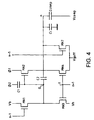
- the gate of the discharge transistor MN3 is connected from classical way to the n + 1 stage and one of its electrodes connected to the voltage Vh which is chosen at a low level or a high level based of the voltage Vb.
- the embodiment shown in FIG. uses a sixth semiconductor device MN7 connected between the line of output n and the output voltage Vgoff, to keep the output line at a low level.
- this semiconductor device consisting of a MOS transistor has its gate connected to the previous stage n-1 so as to reset the CI capacity to the Vgoff voltage each time you go from stage n-1 on stage n or vice versa.
- the shift register stage described with reference to FIG. 4 has the disadvantage of being sensitive to current leakage through the transistors MN1 or MN3 depending on the direction of operation. Indeed, in the embodiment of FIG. 3, the voltage V- is in general less than the voltage Vgoff so that, in a non-selected stage, the transistor output MN2 has a sufficiently low output current not to load the CI capacity when the clock becomes positive. Typically, for amorphous silicon based transistors, V- ⁇ Vgoff - 2 volts.
- the gate of transistor MN1 is connected to the output line of the previous stage n-1 through a coupling capacitor C5 and a diode-mounted MOS transistor MN5 is connected between the common point between the capacitor C5 and the grid of the transistor MN1 and the point G.
- the discharge transistor MN3 is connected to the next floor n + 1 via a capacitance of coupling C6 and also includes a "clamp" diode consisting of a MN6 transistor.
- the node G is connected to the voltage V1.
- the transistors MN1 and MN3 play a symmetrical role to operate the bi-directional stage.
Landscapes
- Shift Register Type Memory (AREA)
- Control Of Indicators Other Than Cathode Ray Tubes (AREA)
- Liquid Crystal Display Device Control (AREA)
Claims (7)
- Schieberegister mit mehreren in Kaskade angeordneten Stufen (n-1, n, n+1), wobei jede Stufe (n) einen Ausgang in Höhe eines ersten Knotens (D) aufweist und mit dem Ausgang der vorhergehenden Stufe (n-1), mit dem Ausgang der nachfolgenden Stufe (n+1) und mit Mitteln verbunden ist, die erste und zweite Taktsignale (1, 2) liefern, wobei die Stufe eine erste Ausgangs-Halbleitervorrichtung (MN2) aufweist, die den Ausgang (n) zwischen hohen und niedrigen Werten des ersten Taktsignals (1) umschaltet, wobei die erste Halbleitervorrichtung vom Potential eines zweiten Knotens (G) gesteuert wird, der seinerseits verbunden ist mit:dadurch gekennzeichnet, dass die Stufe weiter verbunden ist mitdem das zweite Taktsignal (2) liefernden Mittel über einen ersten Kondensator;einem ersten hohen oder niedrigen Potential (Vh) über eine zweite Halbleitervorrichtung (MN3), die vom Ausgang der nachfolgenden Stufe (n+1) gesteuert wird, undeinem zweiten hohen oder niedrigen Potential (Vb) über eine dritte Halbleitervorrichtung (MN1), die vom Ausgang der vorhergehenden Stufe (n-1) gesteuert wird.
- Register nach Anspruch 1, dadurch gekennzeichnet, dass es eine sechste Halbleitervorrichtung (MN7) aufweist, die zwischen die Ausgangsleitung und eine negative Spannung (Vgoff) geschaltet ist, wobei die sechste Halbleitervorrichtung vom Ausgang der vorhergehenden Stufe gesteuert wird.
- Register nach einem der Ansprüche 1 und 2, dadurch gekennzeichnet, dass der Ausgang (n) der Stufe mit einer negativen Spannung (Vgoff) über eine vierte Halbleitervorrichtung (MN4) verbunden ist, die vom Ausgang der nachfolgenden Stufe (n+1) oder der zweiten nachfolgenden Stufe (n+2) gesteuert wird.
- Register nach einem der Ansprüche 1 bis 3, dadurch gekennzeichnet, dass:der zweite Knoten (G) mit der Spannung (V1) verbunden istund dass es Mittel aufweist, um die Steuerspannung der zweiten und dritten Halbleitervorrichtung auf einen Wert von höchstens Null zu blockieren.
- Register nach Anspruch 4, dadurch gekennzeichnet, dass die Mittel aus einem Kondensator (C5, C6) bestehen, der zwischen die Steuerung der Halbleitervorrichtung (MN1, MN3) und den Knoten (G) geschaltet ist, wobei eine fünfte und eine sechste Halbleitervorrichtung (MN5, MN6) je zwischen die Steuerung der zweiten bzw. dritten Halbleitervorrichtung und den Knoten (G) geschaltet sind und wobei die fünfte und sechste Halbleitervorrichtung (MN5, MN6) von der Spannung (V1) des Knotens (G) gesteuert werden.
- Register nach einem der Ansprüche 1 bis 5, dadurch gekennzeichnet, dass die Halbleitervorrichtungen aus MIS-Transistoren, vorzugsweise TFT-Transistoren bestehen.
- Register nach einem der Ansprüche 1 bis 6, dadurch gekennzeichnet, dass die Taktsignale (1, 2) durch ein gleiches Taktsignal in Gegenphase erhalten werden.
Applications Claiming Priority (3)
| Application Number | Priority Date | Filing Date | Title |
|---|---|---|---|
| FR9600260 | 1996-01-11 | ||
| FR9600260A FR2743662B1 (fr) | 1996-01-11 | 1996-01-11 | Perfectionnement aux registres a decalage utilisant des transistors mis de meme polarite |
| EP97900253A EP0815562B1 (de) | 1996-01-11 | 1997-01-09 | Verbessertes schieberegister mit mis-transistoren der gleichen priorität |
Related Parent Applications (1)
| Application Number | Title | Priority Date | Filing Date |
|---|---|---|---|
| EP97900253A Division EP0815562B1 (de) | 1996-01-11 | 1997-01-09 | Verbessertes schieberegister mit mis-transistoren der gleichen priorität |
Publications (3)
| Publication Number | Publication Date |
|---|---|
| EP1156491A2 EP1156491A2 (de) | 2001-11-21 |
| EP1156491A3 EP1156491A3 (de) | 2003-11-05 |
| EP1156491B1 true EP1156491B1 (de) | 2005-03-23 |
Family
ID=9488037
Family Applications (1)
| Application Number | Title | Priority Date | Filing Date |
|---|---|---|---|
| EP01119573A Expired - Lifetime EP1156491B1 (de) | 1996-01-11 | 1997-01-09 | Verbesserungen an Schieberegistern unter alleiniger Verwendung von "MIS" Transistoren |
Country Status (4)
| Country | Link |
|---|---|
| EP (1) | EP1156491B1 (de) |
| JP (1) | JP4035548B2 (de) |
| KR (1) | KR100450865B1 (de) |
| DE (2) | DE69713687T2 (de) |
Families Citing this family (14)
| Publication number | Priority date | Publication date | Assignee | Title |
|---|---|---|---|---|
| KR100685307B1 (ko) * | 1999-11-05 | 2007-02-22 | 엘지.필립스 엘시디 주식회사 | 쉬프트 레지스터 |
| JP3866070B2 (ja) * | 2000-10-20 | 2007-01-10 | 株式会社 日立ディスプレイズ | 表示装置 |
| KR100853720B1 (ko) * | 2002-06-15 | 2008-08-25 | 삼성전자주식회사 | 비정질-실리콘 박막 트랜지스터 게이트 구동 쉬프트레지스터 및 이를 가지는 액정 표시 장치 |
| TW200703224A (en) * | 2005-03-22 | 2007-01-16 | Koninkl Philips Electronics Nv | A shift register circuit |
| ATE443914T1 (de) * | 2005-07-26 | 2009-10-15 | Koninkl Philips Electronics Nv | Multi-input-kreis |
| FR2920907B1 (fr) * | 2007-09-07 | 2010-04-09 | Thales Sa | Circuit de commande des lignes d'un ecran plat a matrice active. |
| RU2458460C2 (ru) | 2007-12-28 | 2012-08-10 | Шарп Кабусики Кайся | Полупроводниковое устройство и дисплейное устройство |
| CN103036548B (zh) | 2007-12-28 | 2016-01-06 | 夏普株式会社 | 半导体装置和显示装置 |
| BRPI0819443A2 (pt) | 2007-12-28 | 2015-05-05 | Sharp Kk | Circuito de acionamento da linha de capacitor de armazenamento e dispositivo de display |
| WO2009084280A1 (ja) | 2007-12-28 | 2009-07-09 | Sharp Kabushiki Kaisha | 表示駆動回路、表示装置及び表示駆動方法 |
| FR2975213B1 (fr) * | 2011-05-10 | 2013-05-10 | Trixell Sas | Dispositif d'adressage de lignes d'un circuit de commande pour matrice active de detection |
| CN102800272B (zh) * | 2011-05-27 | 2016-07-06 | 凌巨科技股份有限公司 | 显示装置的驱动电路 |
| US9412764B2 (en) | 2012-11-28 | 2016-08-09 | Semiconductor Energy Laboratory Co., Ltd. | Semiconductor device, display device, and electronic device |
| CN103943054B (zh) | 2014-01-27 | 2016-07-13 | 上海中航光电子有限公司 | 栅极驱动电路、tft阵列基板、显示面板及显示装置 |
Family Cites Families (2)
| Publication number | Priority date | Publication date | Assignee | Title |
|---|---|---|---|---|
| US5282234A (en) * | 1990-05-18 | 1994-01-25 | Fuji Photo Film Co., Ltd. | Bi-directional shift register useful as scanning registers for active matrix displays and solid state image pick-up devices |
| FR2720185B1 (fr) * | 1994-05-17 | 1996-07-05 | Thomson Lcd | Registre à décalage utilisant des transistors M.I.S. de même polarité. |
-
1997
- 1997-01-09 KR KR1019970706365A patent/KR100450865B1/ko not_active Expired - Lifetime
- 1997-01-09 DE DE69713687T patent/DE69713687T2/de not_active Expired - Lifetime
- 1997-01-09 DE DE69732867T patent/DE69732867T2/de not_active Expired - Lifetime
- 1997-01-09 EP EP01119573A patent/EP1156491B1/de not_active Expired - Lifetime
-
2005
- 2005-11-28 JP JP2005341578A patent/JP4035548B2/ja not_active Expired - Lifetime
Also Published As
| Publication number | Publication date |
|---|---|
| EP1156491A3 (de) | 2003-11-05 |
| DE69732867D1 (de) | 2005-04-28 |
| KR19980702957A (ko) | 1998-09-05 |
| JP2006127751A (ja) | 2006-05-18 |
| KR100450865B1 (ko) | 2005-01-13 |
| DE69713687T2 (de) | 2003-02-06 |
| EP1156491A2 (de) | 2001-11-21 |
| DE69732867T2 (de) | 2006-04-13 |
| JP4035548B2 (ja) | 2008-01-23 |
| DE69713687D1 (de) | 2002-08-08 |
Similar Documents
| Publication | Publication Date | Title |
|---|---|---|
| EP0815562B1 (de) | Verbessertes schieberegister mit mis-transistoren der gleichen priorität | |
| EP0760149B1 (de) | Schieberegister mit gleich polarisierten mis-transistoren | |
| EP1156491B1 (de) | Verbesserungen an Schieberegistern unter alleiniger Verwendung von "MIS" Transistoren | |
| EP0586398B1 (de) | Shiftregister zum abtasten der ansteurungsleitungen zur verwendung bei einer flüssigkristallanzeige | |
| KR100470881B1 (ko) | 전기회로 | |
| EP0237365B1 (de) | Lichtempfindliche Vorrichtung | |
| EP2013863B1 (de) | Organisches elektrolumineszenzdisplay | |
| KR100470882B1 (ko) | 시프트레지스터 및 전자장치 | |
| US6600472B1 (en) | Liquid crystal display device | |
| EP0815552B1 (de) | Flachschirmadressierungsverfahren mit bildelementvorladung, steuereinrichtung zur durchführung des verfahrens und anwendung in grossbildschirmen | |
| US8139055B2 (en) | Combined image sensor and display device | |
| US9123613B2 (en) | Image sensor and display | |
| US20090072158A1 (en) | Method of detecting x-rays and x-ray detecting apparatus | |
| FR2626705A1 (fr) | Montage d'affichage a matrice integree | |
| EP0233489B1 (de) | Verfahren zur Adressierung mindestens eines photoempfindlichen Pixels or eines Flüsigkristallpixels in einer Matrixanordnung | |
| EP0972282B1 (de) | Vorrichtung zur steuerung einer matrixanzeigestelle | |
| EP0487389A1 (de) | Flacher Bildschirm mit aktiver Matrix | |
| EP3925208B1 (de) | Array-detektor mit verringertem gerade/ungerade -effekt | |
| US7095005B2 (en) | Image reading device for reversing polarity of stored charge in capacitor | |
| FR2615993A1 (fr) | Procede et dispositif d'elimination de couplage dans des ecrans a cristaux liquides a transistors en couches minces adresses matriciellement | |
| FR2488016A1 (fr) | Module elementaire pour panneau d'affichage matriciel et panneau d'affichage comportant un tel module | |
| den Boer | 6.2: A Select Line Driver for the Offset‐Scan‐and‐Hold Dual Select Diode AMLCDs | |
| EP0633665A2 (de) | Inverterschaltung |
Legal Events
| Date | Code | Title | Description |
|---|---|---|---|
| PUAI | Public reference made under article 153(3) epc to a published international application that has entered the european phase |
Free format text: ORIGINAL CODE: 0009012 |
|
| 17P | Request for examination filed |
Effective date: 20010816 |
|
| AC | Divisional application: reference to earlier application |
Ref document number: 815562 Country of ref document: EP |
|
| AK | Designated contracting states |
Kind code of ref document: A2 Designated state(s): DE FR GB IT NL |
|
| PUAL | Search report despatched |
Free format text: ORIGINAL CODE: 0009013 |
|
| AK | Designated contracting states |
Kind code of ref document: A3 Designated state(s): DE FR GB IT NL |
|
| RIC1 | Information provided on ipc code assigned before grant |
Ipc: 7G 09G 3/36 B Ipc: 7G 11C 19/28 A |
|
| GRAP | Despatch of communication of intention to grant a patent |
Free format text: ORIGINAL CODE: EPIDOSNIGR1 |
|
| AKX | Designation fees paid |
Designated state(s): DE FR GB IT NL |
|
| GRAS | Grant fee paid |
Free format text: ORIGINAL CODE: EPIDOSNIGR3 |
|
| RAP1 | Party data changed (applicant data changed or rights of an application transferred) |
Owner name: THALES AVIONICS LCD S.A. |
|
| GRAA | (expected) grant |
Free format text: ORIGINAL CODE: 0009210 |
|
| AC | Divisional application: reference to earlier application |
Ref document number: 0815562 Country of ref document: EP Kind code of ref document: P |
|
| AK | Designated contracting states |
Kind code of ref document: B1 Designated state(s): DE FR GB IT NL |
|
| PG25 | Lapsed in a contracting state [announced via postgrant information from national office to epo] |
Ref country code: NL Free format text: LAPSE BECAUSE OF FAILURE TO SUBMIT A TRANSLATION OF THE DESCRIPTION OR TO PAY THE FEE WITHIN THE PRESCRIBED TIME-LIMIT Effective date: 20050323 Ref country code: IT Free format text: LAPSE BECAUSE OF FAILURE TO SUBMIT A TRANSLATION OF THE DESCRIPTION OR TO PAY THE FEE WITHIN THE PRESCRIBED TIME-LIMIT;WARNING: LAPSES OF ITALIAN PATENTS WITH EFFECTIVE DATE BEFORE 2007 MAY HAVE OCCURRED AT ANY TIME BEFORE 2007. THE CORRECT EFFECTIVE DATE MAY BE DIFFERENT FROM THE ONE RECORDED. Effective date: 20050323 |
|
| REG | Reference to a national code |
Ref country code: GB Ref legal event code: FG4D Free format text: NOT ENGLISH |
|
| REF | Corresponds to: |
Ref document number: 69732867 Country of ref document: DE Date of ref document: 20050428 Kind code of ref document: P |
|
| GBT | Gb: translation of ep patent filed (gb section 77(6)(a)/1977) |
Effective date: 20050420 |
|
| NLV1 | Nl: lapsed or annulled due to failure to fulfill the requirements of art. 29p and 29m of the patents act | ||
| PLBE | No opposition filed within time limit |
Free format text: ORIGINAL CODE: 0009261 |
|
| STAA | Information on the status of an ep patent application or granted ep patent |
Free format text: STATUS: NO OPPOSITION FILED WITHIN TIME LIMIT |
|
| 26N | No opposition filed |
Effective date: 20051227 |
|
| REG | Reference to a national code |
Ref country code: FR Ref legal event code: PLFP Year of fee payment: 20 |
|
| PGFP | Annual fee paid to national office [announced via postgrant information from national office to epo] |
Ref country code: DE Payment date: 20160128 Year of fee payment: 20 |
|
| PGFP | Annual fee paid to national office [announced via postgrant information from national office to epo] |
Ref country code: FR Payment date: 20160128 Year of fee payment: 20 Ref country code: GB Payment date: 20160201 Year of fee payment: 20 |
|
| REG | Reference to a national code |
Ref country code: DE Ref legal event code: R071 Ref document number: 69732867 Country of ref document: DE |
|
| REG | Reference to a national code |
Ref country code: GB Ref legal event code: PE20 Expiry date: 20170108 |
|
| PG25 | Lapsed in a contracting state [announced via postgrant information from national office to epo] |
Ref country code: GB Free format text: LAPSE BECAUSE OF EXPIRATION OF PROTECTION Effective date: 20170108 |