EP1158559A2 - Ecran à plasma avec luminophore activé par du terbium(III) - Google Patents
Ecran à plasma avec luminophore activé par du terbium(III) Download PDFInfo
- Publication number
- EP1158559A2 EP1158559A2 EP01000149A EP01000149A EP1158559A2 EP 1158559 A2 EP1158559 A2 EP 1158559A2 EP 01000149 A EP01000149 A EP 01000149A EP 01000149 A EP01000149 A EP 01000149A EP 1158559 A2 EP1158559 A2 EP 1158559A2
- Authority
- EP
- European Patent Office
- Prior art keywords
- phosphor
- plasma
- green
- gas
- xenon
- Prior art date
- Legal status (The legal status is an assumption and is not a legal conclusion. Google has not performed a legal analysis and makes no representation as to the accuracy of the status listed.)
- Ceased
Links
Images
Classifications
-
- H—ELECTRICITY
- H01—ELECTRIC ELEMENTS
- H01J—ELECTRIC DISCHARGE TUBES OR DISCHARGE LAMPS
- H01J11/00—Gas-filled discharge tubes with alternating current induction of the discharge, e.g. alternating current plasma display panels [AC-PDP]; Gas-filled discharge tubes without any main electrode inside the vessel; Gas-filled discharge tubes with at least one main electrode outside the vessel
- H01J11/20—Constructional details
- H01J11/34—Vessels, containers or parts thereof, e.g. substrates
- H01J11/42—Fluorescent layers
-
- C—CHEMISTRY; METALLURGY
- C09—DYES; PAINTS; POLISHES; NATURAL RESINS; ADHESIVES; COMPOSITIONS NOT OTHERWISE PROVIDED FOR; APPLICATIONS OF MATERIALS NOT OTHERWISE PROVIDED FOR
- C09K—MATERIALS FOR MISCELLANEOUS APPLICATIONS, NOT PROVIDED FOR ELSEWHERE
- C09K11/00—Luminescent materials, e.g. electroluminescent or chemiluminescent
- C09K11/08—Luminescent materials, e.g. electroluminescent or chemiluminescent containing inorganic luminescent materials
- C09K11/77—Luminescent materials, e.g. electroluminescent or chemiluminescent containing inorganic luminescent materials containing rare earth metals
- C09K11/7766—Luminescent materials, e.g. electroluminescent or chemiluminescent containing inorganic luminescent materials containing rare earth metals containing two or more rare earth metals
- C09K11/778—Borates
-
- C—CHEMISTRY; METALLURGY
- C09—DYES; PAINTS; POLISHES; NATURAL RESINS; ADHESIVES; COMPOSITIONS NOT OTHERWISE PROVIDED FOR; APPLICATIONS OF MATERIALS NOT OTHERWISE PROVIDED FOR
- C09K—MATERIALS FOR MISCELLANEOUS APPLICATIONS, NOT PROVIDED FOR ELSEWHERE
- C09K11/00—Luminescent materials, e.g. electroluminescent or chemiluminescent
- C09K11/08—Luminescent materials, e.g. electroluminescent or chemiluminescent containing inorganic luminescent materials
- C09K11/55—Luminescent materials, e.g. electroluminescent or chemiluminescent containing inorganic luminescent materials containing beryllium, magnesium, alkali metals or alkaline earth metals
-
- C—CHEMISTRY; METALLURGY
- C09—DYES; PAINTS; POLISHES; NATURAL RESINS; ADHESIVES; COMPOSITIONS NOT OTHERWISE PROVIDED FOR; APPLICATIONS OF MATERIALS NOT OTHERWISE PROVIDED FOR
- C09K—MATERIALS FOR MISCELLANEOUS APPLICATIONS, NOT PROVIDED FOR ELSEWHERE
- C09K11/00—Luminescent materials, e.g. electroluminescent or chemiluminescent
- C09K11/08—Luminescent materials, e.g. electroluminescent or chemiluminescent containing inorganic luminescent materials
- C09K11/64—Luminescent materials, e.g. electroluminescent or chemiluminescent containing inorganic luminescent materials containing aluminium
-
- H—ELECTRICITY
- H01—ELECTRIC ELEMENTS
- H01J—ELECTRIC DISCHARGE TUBES OR DISCHARGE LAMPS
- H01J2211/00—Plasma display panels with alternate current induction of the discharge, e.g. AC-PDPs
- H01J2211/20—Constructional details
- H01J2211/34—Vessels, containers or parts thereof, e.g. substrates
- H01J2211/42—Fluorescent layers
Definitions
- the invention relates to a plasma screen equipped with a front plate, which has a glass plate on which a dielectric layer and a protective layer are applied, with a carrier plate equipped with a phosphor layer, which comprises a red and a blue phosphor and a green, Tb 3+ - contains activated phosphor, with a rib structure that divides the space between the front plate and the carrier plate into plasma cells, which are filled with a xenon-containing gas, and with one or more electrode arrays on the front plate and the carrier plate for generating silent electrical discharges in the Plasma cells.
- Plasma screens allow color images with high resolution, large screen diagonal and are of compact design.
- a plasma screen has a hermetic closed glass cell, which is filled with a gas, arranged with a grid Electrodes on. Applying an electrical voltage causes a gas discharge that produces light in the ultraviolet range (145 to 185 nm). By Phosphors can convert this light into visible light and through the front panel emitted from the glass cell to the viewer.
- Phosphors are used for plasma screens, which are particularly efficient under vacuum UV excitation.
- green-emitting phosphors are, for example, Zn 2 SiO 4 : Mn (ZSM) or BaAl 12 O 19 : Mn (BAL). Both materials show a saturated, green emission color with a high y value of y> 0.7.
- a disadvantage of both materials is their relatively long decay time t 1/10 , which is, for example, 30 ms for Zn 2 SiO 4 with 2.5% Mn. This is because the transition 4 T 1 ⁇ 6 A 1 relevant for the emission of light is spin-prohibited.
- Tb 3+ -activated phosphors are temperature and photostable, since Tb 3+ is difficult to oxidize to Tb 4+ .
- Another advantage of these phosphors over Mn 2+ -activated phosphors is their shorter decay time t 1/10 , which is between 2 and 10 ms, depending on the host lattice.
- US Pat. No. 6,004,481 therefore describes a green-emitting, Tb 3+ -activated phosphor for applications in plasma screens which has the composition (Y 1-xyz Gd x Tb y Ce z ) BO 3 , where 0.0 ⁇ x ⁇ 0.2, 0.01 ⁇ y ⁇ 0.1 and 0.0 ⁇ z ⁇ 0.1.
- Tb 3+ -activated phosphors A major disadvantage of Tb 3+ -activated phosphors is their yellow-green color point, which has a low y value of y ⁇ 0.62.
- the invention has for its object to provide a plasma screen with a Tb 3+ -activated phosphor, the green pixels provide light with an improved color point.
- a plasma screen equipped with a front plate that has a glass plate on which a dielectric layer and a protective layer are applied, with a carrier plate equipped with a phosphor layer that has a red and a blue phosphor and a green Tb 3 + -activated phosphor, with a rib structure that divides the space between the front plate and the carrier plate into plasma cells that are filled with a xenon-containing gas, and with one or more electrode arrays on the front plate and the carrier plate for generating silent electrical discharges in the plasma cells, the gas containing xenon in a proportion between 5 and 30% by volume.
- the proportion of xenon in the gas is 10% by volume.
- the y value of the color point of Tb 3+ -activated phosphors is surprisingly increased by an increased proportion of xenon in the gas.
- the green pixels of a plasma screen with Tb 3+ -activated phosphor are sufficiently saturated in green.
- the green, Tb 3+ -activated phosphor is selected from the group (In x Gd 1-x ) BO 3 : Tb (0 ⁇ x ⁇ 1), Y 2 SiO 5 : Tb, CeMgAl 11 O.
- Tb (Y 1-x- y Gd x Pr y ) BO 3 : Tb (0 ⁇ x ⁇ 1.0 ⁇ y ⁇ 0.05), GdMgB 5 O 10 : Ce, Tb and LaPO 4 : Ce, Tb.
- Tb 3+ -activated phosphors are particularly efficient, green-emitting phosphors when excited with VUV light.
- the green, Tb 3+ -activated phosphor (Y 1-xy Gd x Pr y ) contains BO 3 : Tb (0 ⁇ x ⁇ 1, 0 ⁇ y ⁇ 0.05).
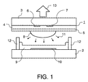
- a plasma cell of an AC plasma display screen with a coplanar arrangement of the electrodes has a front plate 1 and a carrier plate 2.
- the front plate 1 contains a glass plate 3, on which a dielectric layer 4 and a protective layer 5 are applied.
- the protective layer 5 is preferably made of MgO and the dielectric layer 4 is made of PbO-containing glass, for example.
- Parallel, strip-shaped discharge electrodes 6, 7, which are covered by the dielectric layer 4 are applied to the glass plate 3.
- the discharge electrodes 6, 7 are made of metal or ITO, for example.
- the carrier plate 2 is made of glass and parallel, strip-shaped address electrodes 10 made of, for example, Ag are applied to the carrier plate 2 and run perpendicular to the discharge electrodes 6, 7.
- a phosphor layer 9 which emits light in one of the three basic colors red, green or blue.
- the individual plasma cells are separated by a rib structure 12 with separating ribs made of preferably dielectric material.
- a gas preferably a mixture of noble gases, for example of He, Ne or Kr, the xenon in an amount of 5 contains up to 30 vol .-%.
- the dielectric layer 4 over the transparent discharge electrodes 6,7 serves below other with AC plasma screens, a direct discharge between the conductive Material existing discharge electrodes 6.7 and thus the formation of a To prevent the arc from igniting the discharge.
- a Tb 3+ -activated phosphor such as (In x Gd 1-x ) BO 3 : Tb (0 ⁇ x ⁇ 1), Y 2 SiO 5 : Tb, CeMgAl 11 O 19 : is used as the green-emitting phosphor in the phosphor layer.
- (Y 1-xy Gd x Pr y ) BO 3 : Tb (0 x x 1 1, 0 y y 0.0 0.05) is preferably used.
- the gas preferably contains a binary or ternary noble gas mixture of He / Xe, Ne / Xe or He / Ne / Xe with a proportion of xenon in the gas which is between 5 and 30% by volume.
- the proportion of xenon in the gas is very particularly preferably 10% by volume.
- the y-value of the Tb 3+ -activated phosphors is increased by increasing the xenon content in the gas to over 5% by volume. As a result, the green pixels appear sufficiently green.
- Another advantage of plasma screens with a xenon content greater than 5% by volume is that as the xenon content is increased, the intensity of the emission bands of neon in the range of 580 and 750 nm is reduced. This also increases the color saturation of the blue phosphors or pixels.
- a Tb 3+ -activated phosphor in combination with a gas which contains an increased proportion of xenon not only is the y value of the color point of the green pixels increased, but also their luminance is increased.
- the luminance of a monochrome plasma screen with (Y, Gd) BO 3 : Tb as a phosphor increases by almost 30% compared to a monochrome plasma screen with Zn 2 SiO 4 : Mn.
- a suspension of the phosphor (Y, Gd) BO 3 : Tb was prepared, to which additives such as an organic binder and a dispersant were added.
- the suspension was applied in a structured manner to a carrier plate 2 by means of screen printing and dried. This process step is carried out one after the other for the other two types of fluorescent with the emission colors red and blue.
- the carrier plate 2 was made of glass and was equipped with a rib structure 12 and address electrodes 10 made of Ag. All organic additives remaining in the phosphor layers 9 were removed by thermal treatment of the carrier plate 2 at 400 to 600 ° C. in an oxygen-containing atmosphere.
- the support plate 2 was used to build an AC plasma screen used with improved color saturation and color consistency.
Landscapes
- Chemical & Material Sciences (AREA)
- Engineering & Computer Science (AREA)
- Inorganic Chemistry (AREA)
- Materials Engineering (AREA)
- Organic Chemistry (AREA)
- Physics & Mathematics (AREA)
- Plasma & Fusion (AREA)
- Luminescent Compositions (AREA)
- Gas-Filled Discharge Tubes (AREA)
Applications Claiming Priority (2)
| Application Number | Priority Date | Filing Date | Title |
|---|---|---|---|
| DE10024835A DE10024835A1 (de) | 2000-05-19 | 2000-05-19 | Plasmabildschirm mit einem Terbium (III)-aktivierten Leuchtstoff |
| DE10024835 | 2000-05-19 |
Publications (2)
| Publication Number | Publication Date |
|---|---|
| EP1158559A2 true EP1158559A2 (fr) | 2001-11-28 |
| EP1158559A3 EP1158559A3 (fr) | 2004-05-19 |
Family
ID=7642800
Family Applications (1)
| Application Number | Title | Priority Date | Filing Date |
|---|---|---|---|
| EP01000149A Ceased EP1158559A3 (fr) | 2000-05-19 | 2001-05-16 | Ecran à plasma avec luminophore activé par du terbium(III) |
Country Status (7)
| Country | Link |
|---|---|
| US (1) | US6462473B1 (fr) |
| EP (1) | EP1158559A3 (fr) |
| JP (1) | JP2002015674A (fr) |
| KR (2) | KR100961130B1 (fr) |
| CN (1) | CN1218356C (fr) |
| DE (1) | DE10024835A1 (fr) |
| TW (1) | TW507238B (fr) |
Cited By (1)
| Publication number | Priority date | Publication date | Assignee | Title |
|---|---|---|---|---|
| CN100357392C (zh) * | 2003-11-24 | 2007-12-26 | 三星Sdi株式会社 | 用于等离子体显示面板的绿色磷光体 |
Families Citing this family (13)
| Publication number | Priority date | Publication date | Assignee | Title |
|---|---|---|---|---|
| DE10024836A1 (de) * | 2000-05-19 | 2001-11-22 | Philips Corp Intellectual Pty | Plasmabildschirm mit einem Terbium (III)-aktivierten Leuchtstoff |
| DE10104364A1 (de) * | 2001-02-01 | 2002-08-14 | Philips Corp Intellectual Pty | Plasmabildschirm mit einer Leuchtstoffschicht |
| TWI290329B (en) * | 2001-10-30 | 2007-11-21 | Hitachi Ltd | Plasma display device, luminescent device and image and information display system using the same |
| DE10158273A1 (de) * | 2001-11-28 | 2003-06-18 | Philips Intellectual Property | Plasmafarbbildschirm mit grünem Leuchtstoff |
| CN100337296C (zh) * | 2003-01-02 | 2007-09-12 | 三星Sdi株式会社 | 等离子体显示面板 |
| KR100649188B1 (ko) * | 2004-03-11 | 2006-11-24 | 삼성에스디아이 주식회사 | 플라즈마 표시 장치 및 플라즈마 표시 패널의 구동 방법 |
| CN100397544C (zh) * | 2004-05-27 | 2008-06-25 | 株式会社日立制作所 | 发光装置以及使用该发光装置的图像显示装置 |
| JP2006012770A (ja) | 2004-05-27 | 2006-01-12 | Hitachi Ltd | 発光装置及び該発光装置を用いた画像表示装置 |
| US7277018B2 (en) * | 2004-09-17 | 2007-10-02 | Incident Alert Systems, Llc | Computer-enabled, networked, facility emergency notification, management and alarm system |
| KR20080092126A (ko) * | 2007-04-11 | 2008-10-15 | 삼성에스디아이 주식회사 | 플라즈마 디스플레이 장치 |
| JP2009016226A (ja) * | 2007-07-06 | 2009-01-22 | Hitachi Ltd | プラズマディスプレイ装置 |
| JP5244703B2 (ja) * | 2009-05-22 | 2013-07-24 | 昭和電工株式会社 | 発光ダイオード及び発光ダイオードランプ、並びに照明装置 |
| CN103025848B (zh) * | 2010-08-19 | 2014-04-30 | 海洋王照明科技股份有限公司 | 硼酸盐发光材料及其制备方法和应用 |
Family Cites Families (12)
| Publication number | Priority date | Publication date | Assignee | Title |
|---|---|---|---|---|
| JPS5941474B2 (ja) * | 1976-04-30 | 1984-10-06 | 大日本塗料株式会社 | 気体放電発光素子 |
| US5828356A (en) * | 1992-08-21 | 1998-10-27 | Photonics Systems Corporation | Plasma display gray scale drive system and method |
| JPH1062762A (ja) * | 1996-08-22 | 1998-03-06 | Sony Corp | プラズマアドレス液晶表示装置 |
| US6008582A (en) * | 1997-01-27 | 1999-12-28 | Dai Nippon Printing Co., Ltd. | Plasma display device with auxiliary partition walls, corrugated, tiered and pigmented walls |
| KR100290839B1 (ko) * | 1997-06-27 | 2001-10-23 | 구자홍 | 3성분의 혼합가스가 충전된 칼라 피디피 |
| JP3570475B2 (ja) * | 1997-11-26 | 2004-09-29 | Jsr株式会社 | 転写フィルムおよびそれを用いたプラズマディスプレイパネルの製造方法 |
| DE19806213B4 (de) * | 1998-02-16 | 2005-12-01 | Tews, Walter, Dipl.-Chem. Dr.rer.nat.habil. | Kompakte Energiesparlampe |
| US6004481A (en) * | 1998-03-27 | 1999-12-21 | Matsushita Electric Industrial Co., Ltd. | Small particle terbium activated yttrium gadolinium borate phosphors and method of making |
| JP4151104B2 (ja) * | 1998-03-31 | 2008-09-17 | 株式会社日立製作所 | プラズマディスプレイ |
| JP4587567B2 (ja) * | 1998-10-20 | 2010-11-24 | 三星エスディアイ株式会社 | プラズマ表示パネル |
| TW434628B (en) * | 1999-02-24 | 2001-05-16 | Koninkl Philips Electronics Nv | Color display device |
| JP2001228823A (ja) * | 1999-12-07 | 2001-08-24 | Pioneer Electronic Corp | プラズマディスプレイ装置 |
-
2000
- 2000-05-19 DE DE10024835A patent/DE10024835A1/de active Pending
-
2001
- 2001-05-16 CN CN011212659A patent/CN1218356C/zh not_active Expired - Fee Related
- 2001-05-16 EP EP01000149A patent/EP1158559A3/fr not_active Ceased
- 2001-05-16 KR KR1020010026667A patent/KR100961130B1/ko not_active Expired - Fee Related
- 2001-05-16 JP JP2001145753A patent/JP2002015674A/ja active Pending
- 2001-05-18 US US09/860,313 patent/US6462473B1/en not_active Expired - Lifetime
- 2001-08-09 TW TW090119484A patent/TW507238B/zh not_active IP Right Cessation
-
2007
- 2007-11-27 KR KR1020070121432A patent/KR20070120927A/ko not_active Withdrawn
Cited By (1)
| Publication number | Priority date | Publication date | Assignee | Title |
|---|---|---|---|---|
| CN100357392C (zh) * | 2003-11-24 | 2007-12-26 | 三星Sdi株式会社 | 用于等离子体显示面板的绿色磷光体 |
Also Published As
| Publication number | Publication date |
|---|---|
| US20020047520A1 (en) | 2002-04-25 |
| CN1325124A (zh) | 2001-12-05 |
| TW507238B (en) | 2002-10-21 |
| CN1218356C (zh) | 2005-09-07 |
| KR20010105212A (ko) | 2001-11-28 |
| DE10024835A1 (de) | 2001-11-22 |
| KR100961130B1 (ko) | 2010-06-07 |
| EP1158559A3 (fr) | 2004-05-19 |
| JP2002015674A (ja) | 2002-01-18 |
| US6462473B1 (en) | 2002-10-08 |
| KR20070120927A (ko) | 2007-12-26 |
Similar Documents
| Publication | Publication Date | Title |
|---|---|---|
| DE69824053T2 (de) | Lumineszenzmittel, pulverförmiges Lumineszenzmittel, Plasma-Anzeigetafel, und Herstellungsverfahren derselben | |
| JP4904307B2 (ja) | 蛍光層を有するプラズマ画像スクリーン | |
| DE10009915A1 (de) | Plasmabildschirm mit UV-Licht emittierender Schicht | |
| DE19534075A1 (de) | Phosphor und Fluoreszenzanzeigevorrichtung | |
| DE10024836A1 (de) | Plasmabildschirm mit einem Terbium (III)-aktivierten Leuchtstoff | |
| EP1158559A2 (fr) | Ecran à plasma avec luminophore activé par du terbium(III) | |
| EP1256616B1 (fr) | Panneau de visualisation à plasma avec luminophore bleu | |
| DE19962029A1 (de) | Plasmabildschirm mit rotem Leuchtstoff | |
| EP1130621A2 (fr) | Panneau de visualisation à plasma avec luminophore bleu | |
| EP1449236B1 (fr) | Lampe a decharge a barriere dielectrique a restitution de couleurs amelioree | |
| EP1187167B1 (fr) | Panneau d'affichage à couleurs avec couche luminescente bleue | |
| DE60313312T2 (de) | Plasmaanzeigetafel enthaltend eine terbium(iii)-aktivierte fluoreszierende substanz | |
| DE10146798A1 (de) | Plasmabildschirm mit erhöhter Effizienz | |
| EP1103591A1 (fr) | Panneau de visualisation à plasma avec luminophore rouge | |
| DE60204724T2 (de) | Plasmabildschirm mit grünem phosphor | |
| EP1258902A2 (fr) | Panneau d'affichage à plasma ayant un point de couleur blanche amélioré | |
| DE60316087T2 (de) | Plasma-Anzeigetafel mit grünem Leuchtstoff aus Aluminatmischung mit Spinelstruktur | |
| DE102004054091A1 (de) | Durch Vakuum-ultraviolett angeregtes grünes Phosphormaterial und eine dieses Material verwendende Vorrichtung | |
| DE10254175A1 (de) | Plasmabildschirm mit blauemittierendem Leuchtstoff | |
| DE10215891A1 (de) | Plasmabildschirm mit erhöhter Effizienz | |
| DE10210043A1 (de) | Plasmabildschirm mit Pr(III)-aktiviertem Leuchtstoff | |
| EP2351065B1 (fr) | Lampe à décharge basse pression | |
| EP1229099A2 (fr) | Panneau d'affichage à plasma avec couche luminescente | |
| DE10135692A1 (de) | Plasmabildschirm mit erhöhter Effizienz | |
| DE10254208A1 (de) | Dielektrische Barriere-Entladungslampe und Verwendung dieser Lampe für die Röntgenbildbetrachtung |
Legal Events
| Date | Code | Title | Description |
|---|---|---|---|
| PUAI | Public reference made under article 153(3) epc to a published international application that has entered the european phase |
Free format text: ORIGINAL CODE: 0009012 |
|
| AK | Designated contracting states |
Kind code of ref document: A2 Designated state(s): AT BE CH CY DE DK ES FI FR GB GR IE IT LI LU MC NL PT SE TR |
|
| AX | Request for extension of the european patent |
Free format text: AL;LT;LV;MK;RO;SI |
|
| RAP1 | Party data changed (applicant data changed or rights of an application transferred) |
Owner name: KONINKLIJKE PHILIPS ELECTRONICS N.V. Owner name: PHILIPS CORPORATE INTELLECTUAL PROPERTY GMBH |
|
| RAP1 | Party data changed (applicant data changed or rights of an application transferred) |
Owner name: KONINKLIJKE PHILIPS ELECTRONICS N.V. Owner name: PHILIPS INTELLECTUAL PROPERTY & STANDARDS GMBH |
|
| PUAL | Search report despatched |
Free format text: ORIGINAL CODE: 0009013 |
|
| AK | Designated contracting states |
Kind code of ref document: A3 Designated state(s): AT BE CH CY DE DK ES FI FR GB GR IE IT LI LU MC NL PT SE TR |
|
| AX | Request for extension of the european patent |
Extension state: AL LT LV MK RO SI |
|
| RIC1 | Information provided on ipc code assigned before grant |
Ipc: 7C 09K 11/475 B Ipc: 7H 01J 17/49 B Ipc: 7H 01J 17/20 A |
|
| 17P | Request for examination filed |
Effective date: 20041119 |
|
| AKX | Designation fees paid |
Designated state(s): DE FR GB |
|
| 17Q | First examination report despatched |
Effective date: 20050210 |
|
| APBN | Date of receipt of notice of appeal recorded |
Free format text: ORIGINAL CODE: EPIDOSNNOA2E |
|
| APBR | Date of receipt of statement of grounds of appeal recorded |
Free format text: ORIGINAL CODE: EPIDOSNNOA3E |
|
| APBV | Interlocutory revision of appeal recorded |
Free format text: ORIGINAL CODE: EPIDOSNIRAPE |
|
| APBK | Appeal reference recorded |
Free format text: ORIGINAL CODE: EPIDOSNREFNE |
|
| APBN | Date of receipt of notice of appeal recorded |
Free format text: ORIGINAL CODE: EPIDOSNNOA2E |
|
| APAZ | Date of receipt of statement of grounds of appeal deleted |
Free format text: ORIGINAL CODE: EPIDOSDNOA3E |
|
| APBR | Date of receipt of statement of grounds of appeal recorded |
Free format text: ORIGINAL CODE: EPIDOSNNOA3E |
|
| APBR | Date of receipt of statement of grounds of appeal recorded |
Free format text: ORIGINAL CODE: EPIDOSNNOA3E |
|
| APAF | Appeal reference modified |
Free format text: ORIGINAL CODE: EPIDOSCREFNE |
|
| RAP1 | Party data changed (applicant data changed or rights of an application transferred) |
Owner name: SAMSUNG SDI CO., LTD. |
|
| RAP1 | Party data changed (applicant data changed or rights of an application transferred) |
Owner name: LG ELECTRONICS INC. |
|
| RAP1 | Party data changed (applicant data changed or rights of an application transferred) |
Owner name: LG ELECTRONICS INC. |
|
| APBT | Appeal procedure closed |
Free format text: ORIGINAL CODE: EPIDOSNNOA9E |
|
| STAA | Information on the status of an ep patent application or granted ep patent |
Free format text: STATUS: THE APPLICATION HAS BEEN REFUSED |
|
| 18R | Application refused |
Effective date: 20130906 |