EP1158678A1 - Schaltungsanordnung und Verfahren zur Interpolation von Zeitintervallen und diese Schaltungsanordnung verwendende Takterzeugungsschaltung - Google Patents
Schaltungsanordnung und Verfahren zur Interpolation von Zeitintervallen und diese Schaltungsanordnung verwendende Takterzeugungsschaltung Download PDFInfo
- Publication number
- EP1158678A1 EP1158678A1 EP01250187A EP01250187A EP1158678A1 EP 1158678 A1 EP1158678 A1 EP 1158678A1 EP 01250187 A EP01250187 A EP 01250187A EP 01250187 A EP01250187 A EP 01250187A EP 1158678 A1 EP1158678 A1 EP 1158678A1
- Authority
- EP
- European Patent Office
- Prior art keywords
- signal
- circuit
- timing difference
- input
- clock
- Prior art date
- Legal status (The legal status is an assumption and is not a legal conclusion. Google has not performed a legal analysis and makes no representation as to the accuracy of the status listed.)
- Granted
Links
Images












Classifications
-
- H—ELECTRICITY
- H03—ELECTRONIC CIRCUITRY
- H03K—PULSE TECHNIQUE
- H03K5/00—Manipulating of pulses not covered by one of the other main groups of this subclass
-
- G—PHYSICS
- G06—COMPUTING OR CALCULATING; COUNTING
- G06F—ELECTRIC DIGITAL DATA PROCESSING
- G06F7/00—Methods or arrangements for processing data by operating upon the order or content of the data handled
- G06F7/60—Methods or arrangements for performing computations using a digital non-denominational number representation, i.e. number representation without radix; Computing devices using combinations of denominational and non-denominational quantity representations, e.g. using difunction pulse trains, STEELE computers, phase computers
- G06F7/68—Methods or arrangements for performing computations using a digital non-denominational number representation, i.e. number representation without radix; Computing devices using combinations of denominational and non-denominational quantity representations, e.g. using difunction pulse trains, STEELE computers, phase computers using pulse rate multipliers or dividers pulse rate multipliers or dividers per se
-
- H—ELECTRICITY
- H03—ELECTRONIC CIRCUITRY
- H03K—PULSE TECHNIQUE
- H03K5/00—Manipulating of pulses not covered by one of the other main groups of this subclass
- H03K5/00006—Changing the frequency
-
- H—ELECTRICITY
- H03—ELECTRONIC CIRCUITRY
- H03K—PULSE TECHNIQUE
- H03K5/00—Manipulating of pulses not covered by one of the other main groups of this subclass
- H03K5/13—Arrangements having a single output and transforming input signals into pulses delivered at desired time intervals
- H03K5/133—Arrangements having a single output and transforming input signals into pulses delivered at desired time intervals using a chain of active delay devices
-
- H—ELECTRICITY
- H03—ELECTRONIC CIRCUITRY
- H03K—PULSE TECHNIQUE
- H03K5/00—Manipulating of pulses not covered by one of the other main groups of this subclass
- H03K2005/00013—Delay, i.e. output pulse is delayed after input pulse and pulse length of output pulse is dependent on pulse length of input pulse
- H03K2005/00019—Variable delay
- H03K2005/00058—Variable delay controlled by a digital setting
- H03K2005/00065—Variable delay controlled by a digital setting by current control, e.g. by parallel current control transistors
-
- H—ELECTRICITY
- H03—ELECTRONIC CIRCUITRY
- H03K—PULSE TECHNIQUE
- H03K5/00—Manipulating of pulses not covered by one of the other main groups of this subclass
- H03K2005/00013—Delay, i.e. output pulse is delayed after input pulse and pulse length of output pulse is dependent on pulse length of input pulse
- H03K2005/00019—Variable delay
- H03K2005/00058—Variable delay controlled by a digital setting
- H03K2005/00071—Variable delay controlled by a digital setting by adding capacitance as a load
Definitions
- This invention relates to a signal controlling method and apparatus.
- a conventional signal dividing method for dividing (internally dividing or interpolating) a timing difference is used for multiplying the frequency of clock signals, as disclosed in Publication 1 (Japanese patent application 09-157028 (JP Patent Kokai JP-A-11-4145)).
- the clock signal frequency multiplying circuit is made up of four sets of delay circuits 301 to 304, a phase comparator 309 and a counter 310, in case of 4 X frequency multiplying.
- Each of the first to fourth delay circuits 301 to 304 has its output terminals selected by first to fourth switchers 305 to 308, with the first to fourth delay circuits 301 to 304 being connected in series with one another.
- An UP signal 316 or a DOWN signal 317 is transferred to the counter 310, based on the results of comparison, and a control signal 318 is output from the counter 310 to the first to fourth switchers 305 to 308 to make adjustment so that the first clock 311 will be of the same phase (in-phase) to the fifth clock 315.
- the delay time is equal, with the timing difference of the first to fourth clocks 311 to 314 being equal to one another at one-fourth of the clock period tCK.
- a phase locked loop As a circuit for multiplying the frequency of clock signals, a phase locked loop (PLL) is used.
- PLL phase locked loop
- an output of a voltage-controlled oscillator VCO 322 is frequency-divided by a frequency divider 323, and the resulting signal is compared by a phase comparator 319 to an external clock 324.
- the result of comparison is input as an UP signal 325 or a DOWN signal 326 via a charging pump 320 and a loop filter 321 to the VCO322 to control the VCO 322 so that clocks obtained on frequency-dividing the output of the VCO 322 will be of a frequency equal to a frequency of the external clock 324.
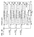
- circuit shown in Fig.24 is a circuit comparing a signal which has traversed the series-connected delay circuits to external clocks approximately several tens of times to correct the delay difference and the phase difference progressively as comparison proceeds.
- the PLL circuit shown in Fig.25, has the drawback that it is insufficient in operating speed, since clocks obtained on frequency division of the output of the VCO 322 will be of a frequency equal to the frequency of the external clock 324, such that a time interval not less than several tens of clock periods must elapse until the clocks multiplied in frequency are obtained.
- the circuit shown in Figs.24 and 25 basically can be used only for clock control, while it cannot be used as a delay circuit for varying the degree of signal delay.
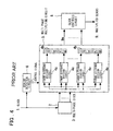
- Fig.4 shows the configuration of the JP-A-11-4145.
- the circuit shown in Fig.4 multiplies the frequency of external clocks. Specifically, the circuit shown in Fig.4 frequency divides external clocks 1 into multi-phase clocks 3 and divides the input timing difference of different phase pulse edges of the multi-phase clocks 3 or multiplexes the clocks 9c of different phases resulting from the division to multiply the phases of the external clock 1.
- the circuit shown in Fig.4 includes a frequency divider 2, a multi-phase clock frequency multiplying circuit 5 and a clock synthesis circuit 8.
- the frequency divider 2 divides the frequency of the external clock 1 to the multi-phase clocks 3.
- a multi-phase clock multiplying circuit 5 includes a timing difference dividing circuit 4a for dividing pulses of different phases of different phase clocks of the multi-phase clocks 3, timing difference dividing circuits 4a for dividing the pulses of the same phase by n and a multiplying circuit 4b for multiplying different phase pulses resulting form division by n, and outputs multi-phase clocks 9a.
- the clock synthesis circuit 8 synthesises the multi-phase clocks 9a, output from the multiplying circuit 4b, to generate single-phase clocks 9.
- the timing difference dividing circuits 4a are connected in parallel with one another.
- the external clocks 1 are frequency divided by the frequency divider 2 into the multi-phase clocks 3, and the input timing difference of different phase pulse edges of the frequency divided multi-phase clocks 3 is divided by a timing difference dividing circuit 4a.
- the resulting clocks 9c of different phases, obtained on frequency division, are multiplexed to multiply the external clock 1, to multiply the phases of the multi-phase clocks.
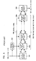
- Fig.5 shows an illustrative structure of a two-phase clock multiplying circuit as the multi-phase clock frequency multiplying circuit 5.
- the two-phase clock multiplying circuit divides the frequency of the external clocks 105 by two to output two-phase clocks having the double (2 ⁇ ) frequency.
- a frequency divider 101 divides the frequency of the external clocks 105 by two to generate two-phase clocks D1, D2.
- Plural two-phase clock multiplying circuits 102 1 to 102 n divide the input timing difference of different phase pulse edges of the frequency divided multi-phase clocks D1, D2 (3 of Fig.4), the first stage two-phase clock multiplying circuit 102 1 generates two-phase clock signals D11, D12 obtained on frequency doubling the two-phase clocks D1, D2 from the frequency divider 101.
- the two-phase clock multiplying circuits 102 1 , 102 3 to 102 n-1 each doubles the frequency of the clocks D21, D22 of the previous stage so that two-phase clocks Dn1, Dn2 obtained on 2nX-multiplying the external clocks 105 are obtained by the two phase clock multiplying circuit 102 n of the last stage.
- a clock synthesis circuit 103 synthesises 2nX-multiplied two-phase clocks Dn1, Dn2 output from the last stage two phase clock multiplying circuit 102 n to output multiplied clocks 107.
- a period detection circuit 104 (6 of Fig.4) is fed as an input with the external clocks 105 to output a control signal 106 (7 of Fig.4) to each two-phase clock multiplying circuits 102 1 to 102 n .
- the control signal 106 corrects the clock period dependency of the timing difference dividing circuit contained in each two-phase clock multiplying circuits 102 1 to 102 n for load adjustment.
- the period detection circuit 104 is made up of a ring oscillator of a fixed number of stages and counters and counts the number of oscillations of the ring oscillators during the period of the external clocks 105 to output a control signal 105 depending on the number of counts.
- the two-phase clock multiplying circuits 102 1 to 102 n are freed of fluctuations in characteristics by the control signal 106 from the period detection circuit 104.
- the circuit shown in Fig.5 divides the frequency of the external clocks 105 by a 1/2 frequency divider 101 and doubles the frequency of the clocks D1, D2 by the initial state two-phase clock multiplying circuit 102 1 to generate two-phase clocks D11, D12.
- the similar process is repeatedly carried out in the two-phase clock multiplying circuits 102 2 to 102 n until 2nX two-phase clocks Dn1, Dn2 are ultimately obtained from the last stage two-phase clock multiplying circuits 102 n .
- clocks Dn1, Dn2 are synthesised by the clock synthesis circuit 103 to produce multiplied clocks 107.
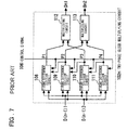
- Fig.7 shows a structure of the two-phase clock multiplying circuit 5. Since the two-phase clock multiplying circuits 102 1 to 102 n are of the same structure, the following explanation is directed to the last stage two-phase clock multiplying circuits 102 n .
- the two-phase clock multiplying circuit 102 n includes parallel-connected first to fourth timing difference dividing circuits 108 to 111 and first and second multiplexing circuits 112, 113.
- Two phase clocks D (n-1) 1, D (n-1) 2 are input to two input ends of the first to fourth timing difference dividing circuits 108 to 111.
- the control signal 106 and four phase clocks P1 to P4 from the timing difference dividing circuits 108 to 111 in the complementary configuration are fed back to the input side.
- the first and second multiplexing circuits 112, 113 are fed with multiplex two-phase clocks P1, P3 and P2, P4 from the first to fourth timing difference dividing circuits 108 to 111 to generate two-phase clocks Dn1, Dn2.
- the two-phase clock multiplying circuit 102 n is fed with two-phase clocks D (n-1) 1 and D (n-1) 2 from the previous stage and with the control signal 106 from the period detection circuit 104 to output frequency doubled two-phase clocks Dn1, Dn2.
- the two-phase clocks D (n-1) 1 and D (n-1) 2 and the control signal 106 are input to the totality of the four timing difference dividing circuits 108 to 111.
- the clocks P1 to P4 are output from the four timing difference dividing circuits 108 to 111 so as to be fed back as inputs to the associated timing difference dividing circuits 108 to 111.
- the rising of the clock P1 is determined by the delay corresponding to the inner time delay of the timing difference dividing circuit 108 as from the rising of the clock D (n-1) 1.
- the rising of the clock P2 is determined by the division of the timing difference between the rising of the clock D (n-1) 1 and that of the two-phase clock D (n-1) 2 and the delay corresponding to the internal delay.
- the rising of the clock P3 is determined by the delay corresponding to the internal delay as from the clock D (n-1) 2.
- the rising of the clock P4 is determined by the division of the timing difference between the rising of the clock D (n-1) 2 and that of the clock D (n-1) 1 and the delay corresponding to the internal delay as from the clock D (n-1) 2.
- the clock P2 controls the decay (falling) of the clock P1 input to the timing difference dividing circuit 108.
- the clock P3 controls the decay of the clock P2 input to the timing difference dividing circuit 109.
- the clock P4 controls the decay of the clock P2 input to the timing difference dividing circuit 110.
- the clock P1 controls the decay of the clock P4 input to the timing difference dividing circuit 111.
- the periods of the clocks P1 to P4 are equal to those of the clocks D (n-1) 1 and D (n-1) 2 such that the clocks P1 to P4 become substantially four-phase signals with a 25% duty.
- the clocks P1, P3 are input to and multiplexed by the multiplexing circuit 112 so as to be output as a clock signal Dn1.
- the clocks P2, P4 are input to and multiplexed by the multiplexing circuit 113 so as to be output as a clock signal Dn2.
- the clocks Dn1, Dn2 are two-phase clocks with subsequently 50% duty, with the periods thereof being one-half those of the clocks D (n-1) 1 and D (n-1) 2.
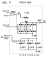
- Figs.9 to 12 typical structures of the timing difference dividing circuits 108 to 111, shown in Fig.7, are explained.
- MP11, MP21, MP31 and MP41 are P-channel MOS transistors
- MN11 to MN19, MN21 to MN29, MN31 to MN39 and MN41 to MN49 are N-channel MOS transistors
- CAP11 to CAP 13 CAP21 to CAP23, CAP31 to CAP33 and CAP41 to CAP43 are capacitance devices.
- the timing difference dividing circuits 108 to 111 are of the identical device structure. That is, each of the difference dividing circuits 108 to 111 is made up of a two-input NAND 10, an inverter 11, a sole P-channel MOS transistor MP11 etc., three sets each of two-series connected N-channel MOS transistors, three sets each of a series-connected N-channel MOS transistor and a capacitance device.
- the three NAND transistors are all of an identical gate width, with the gate width of the three sets of NMOS transistors and the capacitance of the capacitance device being of a size ratio of 1:2:4.
- the difference dividing circuits 108 to 111 are similar in structure, with the difference being the connection of inputs D (n-1) 1 and D (n-2) 2 and the connection of the input P2 (P4).
- the timing difference division circuit 108 includes a NAND circuit NAND11, having a signal D (n-1) 2 and a signal P2 as inputs, a P-channel MOS transistor MP11 having a source, a gate and a drain connected to a power source VCC, to an output end (node 11) of the NAND11 and to an internal node N12, respectively, N-channel MOS transistors MN12, MN13 each having a drain and a gate connected to the inner node N12 and to a signal D (n-1) 1, respectively, a N-channel MOS transistor MN11 having a gate connected to ground potential, and N-channel MOS transistors MN14, MN15 and MN16, having sources commonly connected to the ground potential GND and gates commonly connected to an output end of NAD 11.
- NAND circuit NAND11 having a signal D (n-1) 2 and a signal P2 as inputs
- a P-channel MOS transistor MP11 having a source, a gate and a drain connected to
- the inner node N12 is connected to an input end of an inverter INV11 to output a signal P1 at an output terminal of the inverter INV11.
- the inner node N12 is provided with N-channel MOS transistors MN17, MN18 and MN19, having drains commonly connected and having gates connected to a control signal 106, and with capacitances CAP11, CAP12 and CAP13, having one end connected to a source of N-channel MOS transistors MN17, MN18 and MN19 and having the other ends commonly connected to the ground potential.
- a timing differential circuit 109 includes a NAND circuit NAND 21, fed with a signal D (n-1) 2 and with a signal P3 as inputs, a P-channel MOS transistor MP21, having a source, a gate and a drain connected to the power source VCC, to an output end (node N21) of the NAND21 and to the inner node N22, respectively, an N-channel MOS transistor MN21 having a drain and a gate connected to the inner node N22 and to the signal D (n-1) 1, respectively, N-channel MOS transistors MN22 and MN23, having drains and gates connected commonly to the inner node N22 and to the signal D(n-1)2, respectively, and N-channel MOS transistors MN24, MN25 and MN26 having sources commonly connected to the ground potential GND and gates commonly connected to an output end (node N21) of the NAND21.
- the inner node N22 is connected to the input end of the inverter INV21 to output a signal P3 at an output end of the inverter INV21.
- the inner node N22 includes N-channel MOS transistors MN27, MN28 and MN29 having drains commonly connected and having gates connected to a control signal 106, and capacitances CAP21, CAP22 and CAP23 having one ends connected to sources of N-channel MOS transistors MN27, Mn28 and MN29 and having the other ends commonly connected to the ground potential.
- a timing difference division circuit 110 includes a NAND circuit NAND31, fed with the signal D (n-1) 1 and with a signal P4, as input, a P-channel MOS transistor MP31 having a source, a gate and a drain connected to the power source VCC, to an output end of the NAND31 and to an inner node N32, respectively, N-channel transistors MN32, MN33, having drains commonly connected to the inner node N32 and having gates commonly connected to the signal D (n-1) 2, a N-channel MOS transistor MN31 having a gate connected to the ground potential, and N-channel MOS transistors Mn34, MN35 and MN36 having sources commonly connected to the ground potential GND and having gates commonly connected to the output end of the NAND31.
- the inner node N32 is connected to the input end of the inverter INV31 and outputs a signal P3 at an output end of the inverter INV31.
- the inner node N32 includes N-channel MOS transistors MN37, MN38 and MN39 having drains commonly connected and having gates connected to control signals, and capacitances CAP31, CAP32 and CAP33 having one ends to sources of N-channel MOS transistors MN37, MN38 andMn39 and having the other ends commonly connected to the ground potential.
- a timing difference division circuit 111 includes a NAND circuit NAND41, fed with the signal D (n-1) 1 and with the signal P1, a P-channel MOS transistor MP41 having a source, a drain and a gate connected to the power source VCC, to an output end (node N41) of the NAND41 and to an inner node N42, respectively, an N-channel MOS transistor MN41 having a drain and a gate connected to the internal node N42 and to the signal D (n-1) 2, N-channel MOS transistors MN42, MN43 having drains and gates commonly connected to the inner node N42 and connected to the signal D(n-1)1, respectively, and N-channel MOS transistors MN44, MN45 and MN46 having sources and gates commonly connected to the ground potential GND and commonly connected to an output end of the NAND41, respectively.
- the inner node N41 is connected to an input end of the inverter INV41 and outputs a signal P4 at an output end of the inverter INV41.
- the inner node N42 includes N-channel MOS transistors MN47, MN48 and MN49, having drains commonly connected and also having gates connected to a control signal, and capacitances CAP41, CAP42 and CAP43, having one ends connected to the sources of the N-channel MOS transistors MN47, MN48 and MN49 and having the other ends commonly connected to the ground potential.
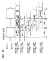
- the operation of the timing difference division circuits 108 to 111 is explained by referring to the timing waveform diagram of Fig.13.
- the timing difference division circuits 108, 110, shown in Figs.9 and 11, are of the same circuit configuration except input/output signal, while the timing difference division circuits 107, 111 shown in Figs.10 and 12 are of the same circuit configuration except the input/output signals. So, operation of the timing difference division circuits 108, 109, shown in Figs.9 and 10 is hereinafter explained.
- one period is from t1 until t3 in Fig.13. So, the inner node waveform for this one period duration is shown.
- the result of extraction of the electrical charges of CV from the clock D (n-1) 1 with the current of 2I, that is CV/2I represents the timing as from the rising edge of the clock D (n-1) 1 until rising of the clock P1.
- the decay of clocks P1 is by the output of the two-input NAND 11 going low to turn ON the P-channel MOS transistor MP11 to charge the inner node N12 to a high level.
- the two-input NAND 11 is fed with a clock D (n-1) 2 and a clock P2, with the output going low when both the clock D (n-1) 2 and the clock P2 are high.
- the period during which the clock P2 is high is comprised within a period during which the clock D (n-1) 2 is high, so that the output clock is of a pattern corresponding to a pattern of the inverted clock P2.
- a logical value is taken of the clock P2 and the clock D (n-1) 2.
- the timing difference division circuit 109 As for the operation of the timing difference division circuit 109, shown in Fig.10, there is shown the internal node waveform during the time period as from t1 until t3 in Fig.13. because this time period corresponds to one period.
- the rise timing of the clock P2 is explained.
- the electrical charges of the node N22 are extracted by the N-channel MOS transistor MN21.
- the residual electrical charges at the node N22 are extracted from the rising edge of the clock D (n-1) 2 by the N-channel MOS transistors MN22, MN23.
- the result of extracting the current CV from the clock D (n-1) 1 during the time period tCKn with the current I, and during the remaining period with 2I, that is tCKn + (CV-tCK ⁇ I)/2I CV + tCKn/2 represents the timing as from the rising edge of the clock D(n-1) 1 until the rising of the clock P2.
- the timing difference with respect to the rising of the clock P1 is just equal to tCKn/2.
- the decay timing of the clock P2 is caused by an output of the two-input NAND 21 going low to turn the P-channel MOS transistor MP21 on to charge the node N22 to high.
- the output of the two-input NAND 21 goes low only when a clock D (n-1) 2 and a clock P3 are fed as inputs and both the clock D (n-1) 2 and the clock P3 are high.
- the clocks P3 and P4 are now explained. Since the timing difference between the rising edge of the clock D (n-1) 1 and that of the clock D (n-1) 2 is tCKn, the rise timing difference between the clocks P1 and P3 is tCKn. So, the rising timing difference between the clocks P2 and P3 is also 1/2tCKn. Similarly, the rising timing difference between clocks P3 and P4 and that between clocks P4 and P1 are also 1/2tCKn.
- the clocks P1 to P4 are four-phase signals of 25% duty, as mentioned previously.
- the clocks P1 and P3 and the clocks P2 and P4 are respectively multiplexed by multiplexing circuits 112, 113, each being comprised of a NOR circuit NOR12 and an inverter INV13, shown in Fig.14, and become two-phase clock signals of 50% duty.
- tCKn is not previously determined by the period of the external clock 1 at the time of designing, so that the current I is fluctuated with device characteristics.
- the CV value is varied depending on the period of the external clock 105 and with device characteristics.
- the gates of the N-channel MOS transistors, connected to the capacitance device (MN17 to MN19 in Fig.9), are fed with a control signal 106, as explained previously, such that the load of the common node N12 can be varied with the control signal 106.
- N-channel MOS transistors and the capacitance devices are set to the size ratio of 1:2:4, eight-stage adjustment is possible.
- the control signal 106 is a value corresponding to the count value of the number of times of oscillations of the ring oscillator, obtained by a counter, during a period of the external clock 105, in a period detection circuit 104.
- the relation between the period of the external clocks and the period of the ring oscillator representative of device characteristics is coded, not only is the operating range not increased relative to the period of the external clocks 1, but also variations in the device characteristics are resolved.
- two-phase clock multiplying circuits 102 1 to 102 n are connected in series, with the frequency of the respective input clocks D1, D to D (n-1) 1 and D (n-1) 2 increasing at a factor of two, so that the capacitance value is adjusted between the two-phase clock multiplying circuits 102 1 to 102 n in order to optimise the CV value.
- multiplied clocks can be generated by dividing the frequency of the external clocks 1 by two to generate two-phase clocks without using feedback circuits, such as PLL or DLL.
- Fig.15 shows a circuit configuration explained as the second embodiment in the JP-A-11-4145 and including a 1/4 frequency divider 201, series-connected four-phase clock multiplying circuits 202 1 to 202 n , a clock synthesis circuit 203 and a period detection circuit 204.
- This circuit divides the external clock signals 205 by the 1/4 frequency divider 201 to generate four-phase clocks Q1 to Q4 which are frequency-doubled by a four-phase clock multiplying circuit 202 1 to generate four-phase clocks Q11 to Q14.
- the similar process is repeated up to four-phase clock multiplying circuits 202 1 to 202 n to generate four-phase clocks Q1 to Q4 frequency multiplied by a factor of 2n.
- These clocks are synthesised by a clock synthesis circuit 203 to generate multiplied clocks 207.
- the period detection circuit 204 is made up of a fixed number of steps of ring oscillators and counters. Specifically, the number of times of oscillation of the ring oscillator during the period of the external clocks 205 is counted by a counter, and a control signal 206 is generated depending on the count value to adjust the load in the four-phase clock multiplying circuits 202 1 to 202 n .
- the period detection circuit 204 the operating range of the external clocks of the circuit and variations in the device characteristics may be resolved.
- the four-phase clock multiplying circuit 202 is explained.
- the four-phase clock multiplying circuits 202 1 to 202 n are of the same configuration.
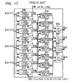
- the four-phase clock multiplying circuit 202 n is made up of eight timing difference division circuits 208 to 215, eight pulse width correction circuits 216 to 223 and four multiplexing circuits 224 to 227.
- the four-phase clock multiplying circuit 202 n is fed with four-phase clocks Q (n-1) 1 to Q (n-1) 4 and a control signal 206 from the period detection circuit 204 to output frequency doubled four-phase clocks Qn1 to Qn4.
- the control signal 206 is input to the eight timing difference division circuits 208 to 215.
- the clocks Q (n-1) to D (n-1) 4 are input to the timing difference division circuits 208, 210, 212, 214, one signal at a time, while being input to the timing difference division circuits 209, 211, 213, 215, two signals at a time.
- Eight clocks T21 to T28 are output from the eight timing difference division circuits 208 to 215.
- the rising of the clocks T21 is determined by the delay corresponding to the internal delay as from the rising of the clock Q (n-1) 1.
- the rising of the clock T22 is determined by the timing division of the rising of the clock Q (n-1) 1 and the rising of the clock Q (n-1) 2 and by the inner delay.
- the rising of the clock T23 is determined by the delay corresponding to the inner delay as from the rising of the clock Q (n-1) 2.
- the rising of the clock T24 is determined by the timing division of the rising of the clock Q (n-1) 2 and the rising of the clock Q (n-1) 3 and by the inner delay.
- the rising of the clock T25 is determined by the delay corresponding to the inner delay as from the rising of the clock Q (n-1) 3.
- the rising of the clock T26 is determined by the timing division of the rising of the clock Q (n-1) 3 and the rising of the clock Q (n-1) 4 and by the inner delay.
- the rising of the clock T27 is determined by the delay corresponding to the inner delay as from the rising of the clock Q (n-1) 4.
- the rising of the clock T28 is determined by the timing division of the rising of the clock Q (n-1) 4 and the rising of the clock Q (n-1) 1 and by the inner delay.
- the clocks T21 and T23 are input to a pulse width correction circuit 216 which then outputs an L pulse P21 having a decaying edge determined by the clock T21 and a rising edge determined by the clock T23.
- pulses p22 to P28 are generated. So, the clocks P21 to P28 are eight pulses with 25% duty respectively dephased by 45°.
- the clocks P25 dephased by 180° from the clock P21, are multiplexed and inverted by the multiplexing circuit 224 and output as 25%-duty clock Qn1.
- clocks Qn2 to Qn4 are generated. So, the clocks Qn1 to Qn4 are 50%-duty four-phase H pulses each with a dephasing of 90 °.
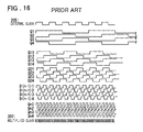
- the period of the clocks Qn1 to Qn4 is just one-half that of the clock Q (n-1) 1 to Q (n-1) 4. That is, the clock frequency is doubled in the course of generating the clocks Qn1 to Qn4 from the clocks Q (n-1) 1 to Q (n-1) 4.
- timing difference division circuits 208 to 215 are of the same circuit configuration.
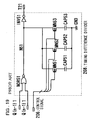
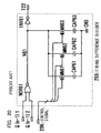
- Figs.19 and 20 show the circuit configuration of the timing difference division circuits 208 and 209, respectively.
- the circuits shown in Figs.19 and 20 are similar in structure except that two inputs are the same signals or two neighbouring signals. That is, input signals to the two-input NOR circuit differ in Figs.19 and 20.
- the timing difference division circuit 208 has an inner node N51, as an output node of the two-input NOR 51, having the same input Q (n-1) 1 as an input.
- the inner node N51 is connected to an input end of the inverter INV51, which outputs T21 at its output end.
- the timing difference division circuit 208 also includes N-channel MOS transistors MN51, MN52 and MN53, having drains commonly connected to the inner node N51, and which are controlled on and off by a control signal 206 from the period detection circuit 204 being coupled to the gates, and capacitances CAP51, CAP52 and CAP53 connected across the sources of the N-channel MOS transistors MN51, MN52 and MN53 and the ground potential.
- the gate widths of the N-channel MOS transistors MN51, MN52 and MN53 and the capacitances CAP51, CAP52 and CAP53 are set to the size ratio of e.g., 1:2:4.
- the clock period is set by eight-stage adjustment of the load connected to the common node based on the control signal 206 output from the period detection circuit 204.
- the timing difference division circuit 209 has an inner node N61, as an output node of the two-input NOR 61, having the same input Q (n-1) 2 as an input.
- the inner node N61 is connected to an input end of the inverter INV61, which outputs T22 at its output end.
- the timing difference division circuit 208 also includes N-channel MOS transistors MN61, MN62 and MN63, having drains commonly connected to the inner node N61, and which are controlled on and off by a control signal 206 from the period detection circuit 204 being coupled to the gates, and capacitances CAP61, CAP62 and CAP63 connected across the sources of the N-channel MOS transistors MN61, MN62 and MN63 and the ground potential.
- the gate widths of the N-channel MOS transistors MN61, MN62 and MN63 and the capacitances CAP61, CAP62 and CAP63 are set to the size ratio of e.g., 1:2:4.
- the clock period is set by eight-stage adjustment of the load connected to the common node based on the control signal 206 output from the period detection circuit 204.
- timing difference division circuits 208, 209 The operation of the timing difference division circuits 208, 209 is now explained by referring to the timing waveform shown in Fig.21.
- the operation of the timing difference division circuit 208 is finished during the time period from tc21 until tc24 of Fig.21. So, the waveform of the inner node N51 during this time period is shown.
- the two-input NOR 51 include two P-channel MOS transistors for connecting input signals IN1, IN2 to the gates, and two N-channel MOS transistors, connected in parallel across the output end and the ground and having gates fed with the input signals IN1, IN2.
- the rising of the clock T21 is by the clock Q (n-1) 1 going low to charge the output node N51 of the two-input NOR51 to high.
- the operation of the timing difference division circuit 209 is well-high finished during the time period from ta21 until ta24 of Fig.21. So, the waveform of the inner node N61 during this time period is shown.
- the rising timing of the output clock T22 is explained.
- the electrical charges of the inner node N22 are extracted by the N-channel MOS transistor.
- the residual electrical charges at the inner node N61 are extracted from the rising edge of the clock Q (n-1) 2 by the N-channel MOS transistors, so that, when the potential of the node N61 reaches the threshold value of the inverter INV61, the edge of the clock T22 rises.
- the result of extracting the current CV from the clock Q (n-1) 1 during the time period I of tCKn with the current I, and during the remaining period with 2I, that is tCKn + (CV-tCKn ⁇ I)/2I CV + tCKn/2 represents the timing as from the rising edge of the clock Q(n-1) until the rising of the clock T22.
- the timing difference with respect to the rising of the clock T21 is just equal to tCKn/2.
- the rising of the clock T22 is by both the clocks Q (n-1) 1 and clocks Q (n-1) 12 going low to charge the output node N61 of the two-input NOR61 high.
- clocks T23 to T28 that is, the rise timing differences of the clocks T21 to T28 are respectively equal to 1/2tCKn.
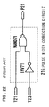
- the pulse width correction circuits 216 to 223 are each made up of an inverter INV71 and a two-input NAND 71, as shown in Fig.22, and generate eight-phase pulses (split signals) P21 to P28, with the duty of 25%, with dephasing being 45 °.
- the multiplexing circuit 224 is comprised of a two-input NAND 81, and generates 50% duty four-phase clocks Qn1 to Qn4, having a dephasing of 90 °, as mentioned previously.
- the period of the clocks Qn1 to Qn4 is just one-half the clock Q (n-1) 1 to Q (n-1) 4.
- the condition required to make the load of the common node N61 variable is the same as that in Fig.9. So, the capacitances and NMOS transistors having the same operating object are used in combination. It is possible not only to increase the operating range for the period of the external clock signals 205 but also to eliminate variations in device characteristics.
- multiplied clocks may be produced by frequency-dividing the external clocks by a factor of four to prepare four-phase clocks at the outset, without using feedback circuits, such as PLL or DLL.
- multiplying circuits may be constructed by fully static simple circuits using basic CMOS devices, such as NAND, NOR or inverters.
- two-phase multiplied clocks are generated from two-phase clocks, while four-phase multiplied clocks are generated from four-phase clocks. It is however possible to connect plural timing difference division circuits in parallel in a tree-like fashion to increase the number of clock phases exponentially to 2, 4 or 8 to generate higher frequency components.
- multiplied clocks may be generated extremely readily by frequency dividing external clocks into multi-phase clocks and taking an intermediate timing of each phase without the necessity of using a loop configuration.
- the time period in which to produce multiplied clocks may be shorter, while the number of required clocks can be predicted at the outset, and hence the queuing time until using the multiplied clocks may be reduced appreciably.
- the capacitance value of the capacitance device is fixed and four-phase clock signals are input, there is a constraint that the capacitance value which is just one half of the input phase difference is in a range from 1:3 for the smallest and largest values, as now explained.
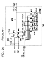
- Fig.26 shows an illustrative structure of a conventional timing difference division circuit.
- the conventional timing difference division circuit includes a logical sum circuit OR1, fed with first and second input signals IN1, IN2, a P-channel MOS transistor MP1, connected across the power source VCC and the inner node N26 and to the gate of which an output signal of the logical sum circuit OR1 is fed, an inverter INV3, for outputting an inverted version of the potential of the inner node N26, and N-channel MOS transistors MN1, MN2, each having a drain connected to the inner node N26, a gate fed with first and second input signals IN1, IN2, respectively, and a source connected to a constant current source I0.
- a control signal 106 output from the period detection circuit is connected to control terminals (gate terminals) of the switching devices MN11 to MN15, comprised of N-channel MOS transistors, to set a capacitance value to be appended to the inner node N26.
- the output of the logical circuit OR1 goes high to turn the P-channel MOS transistor MP1 and the power source path of the inner node N26 and the power source VCC off, while one or both of the N-channel MOS transistors MN1 and MN2 are on, to discharge the inner node N26.
- the potential of the inner node N26 starts to be decreased from the power source potential, until a potential that is not higher than the threshold value of the inverter INV3, the output of the latter starts from low level to high level.
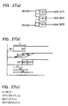
- Fig.27 illustrates the operation of the timing difference division circuit (TMD).
- TMD timing difference division circuit
- two outputs of the first timing difference division circuit (TMD) of the three timing difference division circuits are fed with the same input signal IN1 to output an output signal OUT1.
- the second timing difference division circuit (TMD) is fed with the input signals IN1, IN2 to output an output signal OUT2, while the timing difference division circuit (TMD) is fed at two inputs thereof with the same input signal IN2 to output an output signal OUT3.
- the second timing difference division circuit (TMD) fed with the input signals IN1, IN2 to output the output signal OUT2 is matched to the structure of the timing difference division circuit 209 of Fig.17.
- timing difference division circuit (TMD) commonly fed with IN1 and the timing difference division circuit (TMD) commonly fed with IN2 are configured for being fed with the same signal in Fig.26 and hence is matched to the configuration of the timing difference division circuit 208 of Fig.17.
- Fig.27b shows outputs OUT1 to OUT3 of the first to third timing difference division circuits fed with input signals IN1, IN2 of the timing difference T and changes A1 to A3 of the inner nodes of the first to third timing difference division circuits.
- the first timing difference division circuit (TMD) issues an output signal OUT1 with a delay time t1
- the third timing difference division circuit (TMD) issues an output signal OUT3 with a delay time t3
- the second timing difference division circuit (TMD) issues an output signal OUT2 with a delay time t2
- t3 T + CV/2I. It is noted that electrical charges discharged until the threshold value of the buffer circuit (inverter), to the input end of which is connected the inner node, is exceeded, is denoted CV.
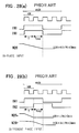
- Fig.28 is a signal waveform diagram showing, for two-phase clocks IN1, IN2 obtained on frequency division of the clocks with the period equal to tCK, the manner of voltage changes in the inner node 26 and input signals in case the in-phase signals and phase signals are input to the timing difference division circuit shown in Fig.26,
- if electrical charges discharged until the threshold value of the inverter INV3 is exceeded are CV, where C is a capacitance value appended to the inner node N26, and V is the threshold voltage t of the inverter INV3, the N-channel MOS transistors MN1, MN2 are turned on, in case of the in-phase input, by the rising of the input signal IN1 from the low level to the high level, to turn the N-channel MOS transistors MN1, MN2 on to discharge the electrical charges with the current 2I.
- the time period during which the N-channel MOS transistors MN1, MN2 are turned on is not longer than 2tCK, so that, if the electrical charges are not extracted during 2tCK, there is produced no output at an output end of the timing difference division circuit.
- the N-channel MOS transistor MN1 is turned on by the rising of the input signal IN1 from the low level to the high level to discharge the electrical charges at the current I.
- the electrical charges of the node N26 that need to be extracted until the threshold value of the inverter INV3 is reached, are CV, and the current with which the electrical charges of the N-channel MOS transistors MN1 and MN2 is I, respectively, the electrical charges CV are extracted with the current I during the phase difference T as from the rising of the first input signal IN1 until the rising of the second input signal IN2 and thereafter with the current 2I.
- the period of extraction with the current 2I is the overlap period Tovp of the first input signal IN1 and the second input signal IN2. If the CV is not completely extracted during this overlap period Tovp, the output of the timing difference division circuit is devoid of the I/2 component of the phase difference T.
- the ratio of the minimum value Cmin to the maximum value Cmax of the value of the capacitance appended to the inner node N26 subjected to charging/discharging is approximately 1:3, as shown in Fig.28, in which the ordinate is the ratio of the interior division of the timing difference division circuit (dividing ratio), which, from the delay time of A1 to A3 in Fig.27b, is equivalent to A2/(A3-A2), and the abscissa is the value of the capacitance appended to the interior node N26.
- the MOS transistors and the MOS capacitance are used to adjust the value of the capacitance of the capacitance device CAP appended to the inner node, there is required an area corresponding to the area of the MOS transistors and the MOS capacitances, thus increasing the chip area.
- timing difference division circuit e.g., interpolator
- the aforementioned circuit unit elongates the overlap period (Tovp) forwardly of a leading edge of the other signal undergoing transition with a delay from the one signal.
- the overlap period (Tovp) may also begin at the leading edge of the other signal and may be further extended from the trailing edge of the one signal so that the overlap period will have an optionally selected value.
- the circuit unit sets the overlap period Tovp so that it begins at the forward edge of the other signal undergoing transition with a delay from the one signal and ends at the trailing edge of the other signal.
- the capacitance of the inner node is made up of plural capacitances (typically of MOS capacitors), the connection of which to the inner node is controlled by a control signal.
- a timing difference division circuit comprising:
- a timing difference division circuit comprising:
- timing difference division circuit of the fifth or sixth aspect the following may be employed.
- the logic circuit outputs, as the first gate signal, a signal the timing of a beginning edge of which is determined by a beginning edge of one of the first and second input signals having a leading phase and the timing of an end edge of which is determined by an end edge of the input signal having a lagging phase; the logic circuit outputting, as the second gate signal, a signal the timing of a beginning edge of which is determined by a beginning edge of one of the first and second input signals having a lagging phase and the timing of an end edge of which is determined by an end edge of the input signal having the lagging phase.
- the logic circuit includes a first gate circuit outputting a first value as the first gate signal when the first and second signals assume first and second values, respectively, or both assume the second value such that both of the first and second signals assume values other than the first value; and a second gate circuit outputting a first value as the second gate signal when the signal of the lagging phase assumes a second value.
- the logic circuit outputs, as the first and second gate signals, an in-phase signal the timing of a beginning edge of which is determined by a beginning edge of one of the first and second input signals having a leading phase and the timing of an end edge of which is determined by an end edge of the input signal having a lagging phase.
- the capacitance values of plural MOS capacitors are connected to the inner node differ from one another.
- the plural MOS transistors of the first conductivity type, the sources and drains of which are connected to the inner node, may be of respectively different gate lengths or gate widths.
- the first and second input signals may be made up of clocks of respectively different phases generated on frequency division of input clock signals; and the control signal fed to the gates of the plural MOS transistors of the first conductivity type, the sources and drains of which are both connected to the inner node, is supplied from a circuit detecting the period of the clocks.
- a clock controlling circuit for generating and outputting multi-phase clocks on frequency division of input clocks; the clock controlling circuit comprising:
- the clock controlling circuit may further comprise a two-phase clock multiplying circuit, wherein the two-phase clock multiplying circuit includes:
- the multi-phase clock multiplying circuit may include
- a signal controlling method in which one of two switches connected in parallel across an inner node and a power source is turned on based on one of two input signals undergoing faster transition to charge or discharge a capacitance of the inner node with a first current
- the overlap period (Tovp) may be elongated forwardly of a leading edge of the other signal undergoing transition with a delay with respect to the one signal or the overlap period (Tovp) is caused to begin at the leading edge of the other signal and to be elongated rearwardly of the trailing edge of the one signal so that the overlap period will have an optional value.
- the overlap period (Tovp) may be caused to begin at the forward edge of the other signal undergoing transition with a delay from the one signal and to end at the trailing edge of the other signal.
- a ninth aspect there is provided a signal controlling method in which first and second input signals with respective different phases are input and an output signal of a delay time determined by a time resulting from division of a timing difference between the two input signals,
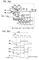
- Fig.1a shows a structure of an embodiment of the present invention and Fig.1b is a timing diagram showing the operation.
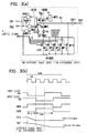
- Fig.2a shows a structure of another embodiment of the present invention and Fig.2b is a timing diagram showing the operation.
- Fig.3a shows a structure of still another embodiment of the present invention and Fig.3b is a timing diagram showing the operation.
- Fig.4 shows a structure of a clock signal-controlling device shown in JP-A-11-4145.
- Fig.5 similarly shows a structure of a clock signal-controlling device shown in JP-A-11-4145.
- Fig.6 is a timing chart for illustrating the operation of the clock signal-controlling device shown in JP-A-11-4145.
- Fig.7 is a circuit diagram showing a two-phase clock multiplexing circuit used in the clock signal-controlling device shown in JP-A-11-4145.
- Fig.8 is a timing chart for illustrating the operation used in the clock signal controlling device shown in JP-A-11-4145.
- Fig.9 is a circuit diagram showing timing difference division circuit used in the clock signal-controlling device shown in JP-A-11-4145.
- Fig.10 is a circuit diagram showing timing difference division circuit used in the clock signal-controlling device shown in JP-A-11-4145.
- Fig.11 is a circuit diagram showing a specified typical timing difference division circuit used in the clock signal-controlling device shown in JP-A-11-4145.
- Fig.12 is a circuit diagram showing another specified typical timing difference division circuit used in the clock signal-controlling device shown in JP-A-11-4145.
- Fig.13 is a timing chart for illustrating the operation of four timing difference division circuits used in the clock signal controlling device shown in JP-A-11-4145.
- Fig.14 is a circuit diagram showing a specified typical multiplexing circuit used in the clock signal-controlling device shown in JP-A-11-4145.
- Fig.15 shows the structure of a clock signal controlling device shown in JP-A-11-4145 (embodiment 2).
- Fig.16 is a timing chart for illustrating the operation of the clock signal controlling device shown in JP-A-11-4145 (embodiment 2).
- Fig.17 is a circuit diagram showing a specified typical four-phase clock multiplying circuit used in the clock signal controlling device shown in JP-A-11-4145 (embodiment 2).
- Fig.18 is a timing chart for illustrating the operation of a four-phase clock multiplying circuit used in the clock signal controlling device shown in JP-A-11-4145 (embodiment 2).
- Fig.19 is a circuit diagram showing a specified typical timing difference division circuit used in the clock signal controlling device shown in JP-A-11-4145 (embodiment 2).
- Fig.20 is a circuit diagram showing a specified typical timing difference division circuit used in the clock signal controlling device shown in JP-A-11-4145 (embodiment 2).
- Fig.21 is a timing chart for illustrating the operation of the timing difference division circuit used in the clock signal controlling device shown in JP-A-11-4145 (embodiment 2).
- Fig.22 is a circuit diagram showing a specified typical pulse width correction circuit used in the clock signal controlling device shown in JP-A-11-4145 (embodiment 2).
- Fig.23 is a circuit diagram showing a specified typical multiplexing circuit used in the clock signal controlling device shown in JP-A-11-4145 (embodiment 2).
- Fig.24 is a circuit diagram showing a conventional clock signal multiplying circuit employing a delay circuit queue.
- Fig.25 is a circuit diagram showing a conventional clock signal multiplying circuit employing a PLL.
- Fig.26 shows a typical circuit configuration of a conventional timing difference division circuit (interpolator).
- Fig.27 (a) to Fig. 27(c) illustrate the operating principle of a timing difference division circuit (interpolator).
- Fig.28 (a) and Fig. 28 (b) show timing charts for illustrating the operation of the conventional timing difference division circuit shown in Fig.26.
- Fig.29 shows a typical relation between the capacitance value and the ratio of interior division in the conventional timing difference division circuit.
- the present invention is directed to a timing difference division circuit at least including two switches MN1, MN2 connected in parallel to control a path between an inner node N1 and a power source on or off, one of the switches MN1 being turned on based on one of two input signals IN1, IN2 undergoing faster transition to charge or discharge a capacitance C appended (connected) to the inner node N1 with a first current (I), the other switch MN2 being turned on based on the other input signal undergoing transition with a delay with respect to the one input signal, the capacitance appended to the inner node being charged or discharged through the one switch in the on-state and the other switch in the on-state with a current value corresponding to a sum (2I) of the first current and a second current; there being provided a buffer circuit INV1 an output logic value of which is changed when the voltage of the inner node exceeds or is smaller than a threshold value.
- the timing difference division circuit includes a circuit unit L1 for setting, based
- a preferred embodiment is directed to a timing difference division circuit L1 including a logic circuit L1 fed with a first input signal and a second input signal IN1, IN2 and outputting first and second gate signals G1, G2, a first MOS transistor MP1 of a first conductivity type, having a source, a drain and a gate connected to a first power source Vcc, an inner node N1 and to the first gate signal G1, respectively, second and third MOS transistors MN1, MN2 of a second conductivity type having drains commonly connected to the inner node and to the gates of which the first and second gate signals G1, G2 are connected, a first constant current source and a second constant current source IO 1 , IO 2 connected across a source of the second MOS transistor MN1 and the second power source and across a source of the third MOS transistor MN2 and the second power source GND, respectively, a plurality of MOS capacitors MP11 to MP14 of the first conductivity type connected to the inner node and a buffer circuit INV
- the logic circuit L1 outputs, as the first gate signal G1, a signal the timing of a beginning edge of which is determined by a beginning edge (leading edge) of one of the first and second input signals IN1, IN2 having a leading phase and the timing of an end edge of which is determined by an end edge (trailing edge) of the input signal having a lagging phase.
- the logic circuit L1 outputs, as the second gate signal, a signal the timing of a beginning edge of which is determined by a beginning edge of one of the first and second input signals having a lagging phase and the timing of an end edge of which is determined by an end edge of the input signal having the lagging phase.
- the timing of the first and second gate signals, output from the logic circuit L1 is adjusted by adjusting the timing at which the second and third MOS transistors MN1, MN2 of the second conductivity type are overlapped and turned on.
- the maximum value Cmax of the capacitance to be appended to the inner node N1 can be varied when two four-phase clocks with the period tCK are input and signals with the delay just equal to 1/2 (2tCK) can be varied.
- the present embodiment of the present invention also features using MOS capacitors MP11 to MP14 as capacitances appended (annexedly connected) to the inner node N1.
- the MOS capacitors MP11 to MP14 are MOS transistors the sources and the drains of which are connected to the inner node N1, and the gates of which are fed with a control signal 7. If, in the case of a p-type semiconductor, the voltage VG applied to the gate, that is the voltage of the control signal 7, is positive, a depletion layer is produced in the semiconductor interface, so that, as an equivalent circuit, there is produced a capacitor comprised of a series connection of the capacitance CD of the depletion layer and the capacitance C0 of the gate oxide film.
- Plural MOS transistors (MP11 to MP14) of the first conductivity type are of respective different gate lengths or gate widths.
- the chip area arranged in an integrated circuit can be smaller than that of a conventional circuit explained with reference to e.g., Fig.26.
- the timing difference division circuit includes a frequency divider 2 (Fig.4) for generating and outputting multi-phase clocks on frequency division of input clocks, a period detection circuit 6 (Fig.4) for detecting the period of the input clock, and a multi-phase multiplying circuit 5 for being fed as input with multi-phase clocks output from the frequency divider to generate multi-phase clocks multiplied from the clocks.
- the multi-phase multiplying circuit includes a plurality of timing difference division circuits for outputting a signal corresponding to division of the timing difference of two inputs and a plurality of multiplexing circuits for multiplexing and outputting outputs of two of the timing difference division circuits.
- the control signal from the period defection circuit is fed as a control signal to the MOS capacitance device connected to an inner node of the timing difference division circuit.
- the clock controlling circuit also includes a two-phase clock multiplying circuit, this two-phase clock multiplying circuit including four timing difference division circuits 108 to 111 of Fig.7 for being fed with two-phase clocks (first and second clocks) and for outputting a signal corresponding to division of the timing difference of two inputs, and two multiplexing circuits for being each fed with outputs of the first and third timing difference division circuits and outputs of the second and fourth timing difference division circuits.
- the timing difference division circuit of the present invention is used as these timing difference division circuits.
- the multi-phase clock multiplying circuit includes 2n timing difference division circuits 208 to 215 (Fig.17) each for being fed with n-phase clocks (first to nth clocks) and for outputting a signal corresponding to the division of the timing difference of two inputs.
- the (2I-1)st timing difference division circuit, where 1 ⁇ I ⁇ n, is fed with the same Ith clocks as the two inputs, whilst the 2Ith timing difference division circuit, where 1 ⁇ I ⁇ n, is fed with the Ith clock and with (I+1 mod n)th clock, as inputs, where mod denotes remainder processing and I+1 mod n means a remainder resulting from division of I+1 by m.
- the multi-phase clock multiplying circuit also includes 2n pulse width correction circuits 216 to 223 fed with an output of the Jth timing difference division circuit, where 1 ⁇ J ⁇ 2n, and with an output of the (J + 2mod n)th timing difference division circuit where n is a remainder obtained on dividing J+2 with n, as inputs, and n multiplexing circuits 224 to 227 each fed with an output of the Kth pulse width correction circuit, where 1 ⁇ K ⁇ n, and with an output of the (K+n)th pulse width correction circuit, as inputs.
- the timing difference division circuit of the present invention is used as these timing difference division circuits.
- the timing difference division circuit also termed an interpolator, includes a logical circuit L1, having an input clock 1 (IN1) and an input clock 2 (IN2) as inputs, a P-channel MOS transistor MP1, having a source, a gate and a drain connected to a power source, to an output G1 (first gate signal) of the logical circuit L1 and to a node N1, respectively, and N-channel MOS transistors MN1, MN2, having drains, gates and sources connected to a common node N1, outputs G1 (first gate signal) and G2 (second gate signal) of the logical circuit L1 and to constant current sources 10 1 , 10 2 , respectively, with the node N1 being connected to an input end of the inverter INV1.
- the current values of the constant current sources 10 1 , 10 2 are equal to each other and set to 1.
- the timing difference division circuit also includes plural P-channel MOS transistors MP11 to MP15, having sources connected commonly, and having drain connected commonly and connected to the node N1.
- a control signal 7 from the period detection circuit 6 of Fig.4 is connected to the gates of the P-channel MOS transistors MP11 to MP15. Control is made so that, if the clock period is large or small, the value of the capacitance appended (connected) to the inner node N1 is increased or decreased, respectively.
- the first gate signal G1 has the timing of a beginning edge (leading edge) determined by a beginning edge of a leading phase input of two-phase inputs of the input clocks 1 and 2, while having the timing of an end edge (trailing edge) determined by the end edge of the lagging phase input.
- the second gate signal G2 has a timing of a beginning edge (leading edge) determined by a beginning edge of a lagging phase input of two-phase inputs of the input clocks 1 and 2, while having the timing of an end edge (trailing edge) determined by the end edge of the lagging phase input.
- An area specified by the gate length (L) or the gate width (W) of the P-channel MOS transistors MP11 to MP15 making up MOS capacitors has a ratio of 1:2:4:8:16, so that the capacitance ratio is 1:2:4:8:16.
- the capacitance values of the P-channel MOS transistors MP11 to MP15 are variably set by the voltage of the control signal 7.
- Fig.1b shows a timing waveform for illustrating the operation of the timing difference division circuit of the embodiment of the present invention shown in Fig.1a.
- Fig.1b shows the waveform of the input clocks 1, 2, at the input terminals IN1, IN2, generated by the logic circuit L1, first and second gate signals G1, G2 generated by the logic circuit L1 and the inner node N1.
- the input clocks 1, 2 are two-phase clocks, with the phase difference (timing difference) equal to T, frequency divided by a 1/4 frequency diving circuit, not shown, from the four-frequency-divided signals of the clocks with the period of 4T exhibiting a phase difference of T from one another.
- the first gate signal G1 has its rising edge determined by the timing of the rising edge of the input clock 1 having a leading phase, while having its falling edge determined by the timing of the falling edge of the input clock 2 with the lagging phase.
- the second gate signal G2 has its rising edge determined by the timing of the rising edge of the input clock 1 having a lagging phase, while having its falling edge determined by the timing of the falling edge of the input clock 2 with the lagging phase.
- Fig.1b shows two sorts of waveforms N1e and N1f, as voltage waveforms of the inner node N1.
- the timing of the output signal OUT to indicate a value equal to division to 1/2 of the phase difference of the input clocks 1 and 2
- N1e and N1f indicate the case where the value of the capacitance connected to the inner node N1 is the minimum capacitance Cmin and the case where the value of the capacitance connected to the inner node N1 is the maximum capacitance Cmax.
- the electrical charge of the inner node N1 that needs to be extracted until the threshold value of the inverter INV1 is exceeded, is CV, and the current with which the electrical charges of the N-channel MOS transistor MN1 are extracted is I, the electrical charge CV is extracted with the current I as from the rising of the first gate signal G1 (voltage of the node nl is decreased).
- the I/2 component of the phase difference T is removed. That is, before rising of the input clock 2, an output signal is output from the timing difference division circuit (inverter INV1), that is the output rises.
- the electrical charge of the node N1 that needs to be extracted until the threshold value Vt of the inverter INV1 is exceeded, is CV, and the current with which the electrical charge of the N-channel MOS transistors MN1 and MN2 is I
- the electrical charge CV is extracted with the current I of the N-channel MOS transistor MN1 during the phase difference T as from the rising of the first gate signal G1 to the rising of the second input signal IN2, and thereafter with the current 2I.
- the size of Cmax can be adjusted by adjusting the length of the overlap period Tovp of the first and second gate signals G1, G2 by the logic circuit L1.
- variable capacitance can be constructed without the necessity of providing the MOS transistor switches (MN11 to MN14) and capacitors (CAP11 to CAP15) shown in Fig.26 etc., thus reducing the chip area.
- the circuit for controlling the overlap of the input clocks is constructed using circuits of the same phase input and circuits of the different phase input using NAND devices.
- the inputs are four-phase clock inputs.
- the input signals are signals IN1 and IN2 having timing differential.
- the constant current sources 10 1 , 10 2 are of an equal current value I.
- the first and second gate signals IN1, IN2 are high as from the falling edge of the signal IN1 until the rising edge of the signal IN2, with the overlap period Tovp being 3tCK.
- the logic circuit L1 includes a NAND circuit NAND11, as a circuit for generating the first gates signal IN1B from the first and second inputs IN1, IN2 as inputs of different phases.
- the logic circuit L1 also includes a NAND circuit NAND12, fed with the second input IN2 and with a fixed high value as inputs, as a circuit for generating the second gate signal IN2B.
- a MOS capacitor device MP2 To the second gate signal IN2B is connected a MOS capacitor device MP2 for counterbalancing the first gate signal IN1B and the load.
- the NAND circuit NAND13 is fed as input with the input IN1 and with the ground potential to counterbalance the loads of the inputs 1 and 2.
- the capacitance value with which the timing difference division circuit is able to provide timing with the interior division ratio of 1/2 of the timing difference is 1:5 from the minimum value to the maximum value. This indicates marked improvement over the conventional value of 1:3 thereby enhancing the range of the operating frequency.
- the above-described timing difference division circuit may be used with advantage in a timing difference division circuit in the clock control circuit shown in Figs.4 to 7 and 15 to 17.
- four-phase clocks are used in the above-described embodiment, eight phase or sixteen phase signals, for example, may, of course, be used.
- the capacitances and switches for controlling the connection of the capacitance to the inner node is removed by replacing the capacitances by MOS capacitors, it is possible to suppress or decrease the chip area.
Landscapes
- Physics & Mathematics (AREA)
- Engineering & Computer Science (AREA)
- Nonlinear Science (AREA)
- General Physics & Mathematics (AREA)
- Theoretical Computer Science (AREA)
- Mathematical Analysis (AREA)
- Computing Systems (AREA)
- Mathematical Optimization (AREA)
- Mathematical Physics (AREA)
- Pure & Applied Mathematics (AREA)
- General Engineering & Computer Science (AREA)
- Computational Mathematics (AREA)
- Manipulation Of Pulses (AREA)
- Dram (AREA)
- Pulse Circuits (AREA)
Applications Claiming Priority (2)
| Application Number | Priority Date | Filing Date | Title |
|---|---|---|---|
| JP2000157167A JP3667196B2 (ja) | 2000-05-26 | 2000-05-26 | タイミング差分割回路 |
| JP2000157167 | 2000-05-26 |
Publications (2)
| Publication Number | Publication Date |
|---|---|
| EP1158678A1 true EP1158678A1 (de) | 2001-11-28 |
| EP1158678B1 EP1158678B1 (de) | 2006-12-13 |
Family
ID=18661848
Family Applications (1)
| Application Number | Title | Priority Date | Filing Date |
|---|---|---|---|
| EP01250187A Expired - Lifetime EP1158678B1 (de) | 2000-05-26 | 2001-05-26 | Schaltungsanordnung und Verfahren zur Interpolation von Zeitintervallen und diese Schaltungsanordnung verwendende Takterzeugungsschaltung |
Country Status (7)
| Country | Link |
|---|---|
| US (1) | US6545518B2 (de) |
| EP (1) | EP1158678B1 (de) |
| JP (1) | JP3667196B2 (de) |
| KR (1) | KR100405019B1 (de) |
| CN (1) | CN1203613C (de) |
| DE (1) | DE60125091T8 (de) |
| TW (1) | TW501345B (de) |
Cited By (2)
| Publication number | Priority date | Publication date | Assignee | Title |
|---|---|---|---|---|
| CN1303510C (zh) * | 2003-10-13 | 2007-03-07 | 凌阳科技股份有限公司 | 光学鼠标的动态影像检索速率的控制方法及装置 |
| CN1333326C (zh) * | 2004-03-12 | 2007-08-22 | 凌阳科技股份有限公司 | 光学鼠标光源亮度控制装置 |
Families Citing this family (25)
| Publication number | Priority date | Publication date | Assignee | Title |
|---|---|---|---|---|
| ES2208279T3 (es) * | 2000-03-15 | 2004-06-16 | Ct-Concept Technologie Ag | Procedimiento para el funcionamiento de una disposicon en paralelo de conmutadores de semiconductores de potencia. |
| JP3636657B2 (ja) * | 2000-12-21 | 2005-04-06 | Necエレクトロニクス株式会社 | クロックアンドデータリカバリ回路とそのクロック制御方法 |
| EP1267525A2 (de) * | 2001-03-16 | 2002-12-18 | Broadcom Corporation | Netzwerkvermittlungsstelle mit programmierbarer Verzögerung und Frequenzverdoppler |
| JP3652304B2 (ja) * | 2001-11-29 | 2005-05-25 | Necマイクロシステム株式会社 | クロック生成回路及びクロック生成方法 |
| US6650159B2 (en) * | 2002-03-29 | 2003-11-18 | Intel Corporation | Method and apparatus for precise signal interpolation |
| US6774683B2 (en) * | 2002-08-13 | 2004-08-10 | Analog Devices, Inc. | Control loop for minimal tailnode excursion of differential switches |
| US6774701B1 (en) * | 2003-02-19 | 2004-08-10 | Raytheon Company | Method and apparatus for electronic switching with low insertion loss and high isolation |
| US6894551B2 (en) * | 2003-09-05 | 2005-05-17 | Micron Technology, Inc. | Multiphase clock generators |
| US7061285B2 (en) * | 2004-04-15 | 2006-06-13 | Woods Paul R | Clock doubler |
| KR100649249B1 (ko) * | 2004-06-30 | 2006-11-24 | 삼성에스디아이 주식회사 | 역다중화 장치와, 이를 이용한 발광 표시 장치 및 그 표시패널 |
| JP4563737B2 (ja) | 2004-07-02 | 2010-10-13 | ルネサスエレクトロニクス株式会社 | パルス幅変調回路 |
| JP4769509B2 (ja) * | 2004-08-02 | 2011-09-07 | パナソニック株式会社 | 半導体装置 |
| JP2006319399A (ja) | 2005-05-10 | 2006-11-24 | Nec Electronics Corp | パルス幅変調回路及び多相クロック生成回路 |
| JP2007124363A (ja) | 2005-10-28 | 2007-05-17 | Nec Electronics Corp | 遅延ロックループ回路 |
| JP2009152682A (ja) * | 2007-12-18 | 2009-07-09 | Ricoh Co Ltd | 位相差平滑化装置 |
| CN101521501B (zh) * | 2008-02-27 | 2012-05-23 | 硕颉科技股份有限公司 | 信号产生装置 |
| US8471754B2 (en) * | 2008-08-01 | 2013-06-25 | Advantest Corporation | Time measurement circuit |
| KR101861728B1 (ko) * | 2012-02-03 | 2018-05-30 | 삼성전자주식회사 | 직류 전원 장치 |
| FR2992484B1 (fr) * | 2012-06-21 | 2015-05-22 | Sagem Defense Securite | Circuit electrique de coupure d'une alimentation electrique a transistors et fusibles |
| JP6461517B2 (ja) * | 2014-08-28 | 2019-01-30 | ルネサスエレクトロニクス株式会社 | 半導体装置 |
| US9473146B2 (en) * | 2015-02-03 | 2016-10-18 | Micron Technology, Inc. | Apparatuses and methods for low power counting circuits |
| US10483956B2 (en) | 2017-07-20 | 2019-11-19 | Rohm Co., Ltd. | Phase interpolator, timing generator, and semiconductor integrated circuit |
| US10270456B1 (en) * | 2018-01-02 | 2019-04-23 | Realtek Semiconductor Corp. | Apparatus and method for frequency tripling |
| KR102536639B1 (ko) * | 2018-08-14 | 2023-05-26 | 에스케이하이닉스 주식회사 | 메모리 장치의 버퍼 제어 회로 |
| WO2020132787A1 (en) * | 2018-12-24 | 2020-07-02 | Zhejiang Dahua Technology Co., Ltd. | System and method for adatpting a polarity of a data signal |
Citations (5)
| Publication number | Priority date | Publication date | Assignee | Title |
|---|---|---|---|---|
| US5327031A (en) * | 1992-03-24 | 1994-07-05 | Bull S.A. | Variable-delay circuit |
| GB2321144A (en) * | 1996-12-31 | 1998-07-15 | Mosaid Technologies Inc | Temperature-insensitive adjustable CMOS fine delay circuit |
| EP0865160A2 (de) * | 1997-03-13 | 1998-09-16 | Nec Corporation | Interpolationsschaltung |
| EP0884732A2 (de) * | 1997-06-12 | 1998-12-16 | Fujitsu Limited | Zeitgeberschaltung, Vorrichtung und System für integrierten Halbleiterschaltkreis unter deren Anwendung und Signalübertragungssystem |
| US6052004A (en) * | 1997-06-13 | 2000-04-18 | Nec Corporation | Method and apparatus for controlling clock signals |
Family Cites Families (12)
| Publication number | Priority date | Publication date | Assignee | Title |
|---|---|---|---|---|
| DE3072118D1 (en) * | 1979-12-26 | 1988-09-22 | Toshiba Kk | A driver circuit for charge coupled device |
| JPS5974724A (ja) * | 1982-10-21 | 1984-04-27 | Sony Corp | パルス発生回路 |
| JPS6454924A (en) * | 1987-08-26 | 1989-03-02 | Sharp Kk | Clock pulse generating circuit |
| JPH01152815A (ja) * | 1987-12-09 | 1989-06-15 | Nec Corp | 周波数逓倍回路 |
| JP3140605B2 (ja) * | 1993-04-28 | 2001-03-05 | 富士通株式会社 | 出力バッファ回路 |
| US5530837A (en) | 1994-03-28 | 1996-06-25 | Hewlett-Packard Co. | Methods and apparatus for interleaving memory transactions into an arbitrary number of banks |
| JPH0818414A (ja) * | 1994-04-26 | 1996-01-19 | Hitachi Ltd | 信号処理用遅延回路 |
| JPH07321613A (ja) * | 1994-05-24 | 1995-12-08 | Kokusai Electric Co Ltd | 周波数逓倍器、波形整形回路、可変位相シフト回路 |
| US5442835A (en) | 1994-06-15 | 1995-08-22 | Jenkins Metal Corporation | Screens for a carding machine |
| JPH1093401A (ja) * | 1996-09-13 | 1998-04-10 | Nec Eng Ltd | クロック周波数逓倍回路 |
| JP3220052B2 (ja) | 1997-06-13 | 2001-10-22 | 日本電気株式会社 | クロック制御装置 |
| JP3415444B2 (ja) * | 1998-06-12 | 2003-06-09 | Necエレクトロニクス株式会社 | クロック制御方法および回路 |
-
2000
- 2000-05-26 JP JP2000157167A patent/JP3667196B2/ja not_active Expired - Fee Related
-
2001
- 2001-04-17 TW TW090109136A patent/TW501345B/zh not_active IP Right Cessation
- 2001-05-23 CN CNB011161760A patent/CN1203613C/zh not_active Expired - Fee Related
- 2001-05-24 US US09/864,735 patent/US6545518B2/en not_active Expired - Lifetime
- 2001-05-25 KR KR10-2001-0028861A patent/KR100405019B1/ko not_active Expired - Fee Related
- 2001-05-26 DE DE60125091T patent/DE60125091T8/de active Active
- 2001-05-26 EP EP01250187A patent/EP1158678B1/de not_active Expired - Lifetime
Patent Citations (5)
| Publication number | Priority date | Publication date | Assignee | Title |
|---|---|---|---|---|
| US5327031A (en) * | 1992-03-24 | 1994-07-05 | Bull S.A. | Variable-delay circuit |
| GB2321144A (en) * | 1996-12-31 | 1998-07-15 | Mosaid Technologies Inc | Temperature-insensitive adjustable CMOS fine delay circuit |
| EP0865160A2 (de) * | 1997-03-13 | 1998-09-16 | Nec Corporation | Interpolationsschaltung |
| EP0884732A2 (de) * | 1997-06-12 | 1998-12-16 | Fujitsu Limited | Zeitgeberschaltung, Vorrichtung und System für integrierten Halbleiterschaltkreis unter deren Anwendung und Signalübertragungssystem |
| US6052004A (en) * | 1997-06-13 | 2000-04-18 | Nec Corporation | Method and apparatus for controlling clock signals |
Non-Patent Citations (1)
| Title |
|---|
| COMBES M ET AL: "A PORTABLE CLOCK MULTIPLIER GENERATOR USING DIGITAL CMOS STANDARD CELLS", IEEE JOURNAL OF SOLID-STATE CIRCUITS,US,IEEE INC. NEW YORK, vol. 31, no. 7, 1 July 1996 (1996-07-01), pages 958 - 965, XP000632382, ISSN: 0018-9200 * |
Cited By (2)
| Publication number | Priority date | Publication date | Assignee | Title |
|---|---|---|---|---|
| CN1303510C (zh) * | 2003-10-13 | 2007-03-07 | 凌阳科技股份有限公司 | 光学鼠标的动态影像检索速率的控制方法及装置 |
| CN1333326C (zh) * | 2004-03-12 | 2007-08-22 | 凌阳科技股份有限公司 | 光学鼠标光源亮度控制装置 |
Also Published As
| Publication number | Publication date |
|---|---|
| KR100405019B1 (ko) | 2003-11-07 |
| DE60125091T2 (de) | 2007-07-05 |
| CN1203613C (zh) | 2005-05-25 |
| CN1333598A (zh) | 2002-01-30 |
| EP1158678B1 (de) | 2006-12-13 |
| US20010045853A1 (en) | 2001-11-29 |
| DE60125091T8 (de) | 2007-11-22 |
| US6545518B2 (en) | 2003-04-08 |
| JP3667196B2 (ja) | 2005-07-06 |
| JP2001339280A (ja) | 2001-12-07 |
| KR20010107751A (ko) | 2001-12-07 |
| DE60125091D1 (de) | 2007-01-25 |
| TW501345B (en) | 2002-09-01 |
Similar Documents
| Publication | Publication Date | Title |
|---|---|---|
| EP1158678B1 (de) | Schaltungsanordnung und Verfahren zur Interpolation von Zeitintervallen und diese Schaltungsanordnung verwendende Takterzeugungsschaltung | |
| KR100465265B1 (ko) | 클럭 제어 방법 및 회로 | |
| JP3450293B2 (ja) | クロック制御回路及びクロック制御方法 | |
| JP3346224B2 (ja) | クロック信号制御装置 | |
| US7180340B2 (en) | Frequency multiplier capable of adjusting duty cycle of a clock and method used therein | |
| WO2002031980A2 (en) | Cyclic phase signal generation from a single clock source using current phase interpolation | |
| JP3220052B2 (ja) | クロック制御装置 | |
| US6967512B2 (en) | Multiphase-clock processing circuit and clock multiplying circuit | |
| US6900684B2 (en) | Pulse processing circuit and frequency multiplier circuit | |
| CN120729248A (zh) | Dcei、小数分频器、占空比校正电路及芯片 |
Legal Events
| Date | Code | Title | Description |
|---|---|---|---|
| PUAI | Public reference made under article 153(3) epc to a published international application that has entered the european phase |
Free format text: ORIGINAL CODE: 0009012 |
|
| AK | Designated contracting states |
Kind code of ref document: A1 Designated state(s): DE GB Kind code of ref document: A1 Designated state(s): AT BE CH CY DE DK ES FI FR GB GR IE IT LI LU MC NL PT SE TR |
|
| AX | Request for extension of the european patent |
Free format text: AL;LT;LV;MK;RO;SI |
|
| 17P | Request for examination filed |
Effective date: 20011009 |
|
| 17Q | First examination report despatched |
Effective date: 20020619 |
|
| AKX | Designation fees paid |
Free format text: DE GB |
|
| RAP1 | Party data changed (applicant data changed or rights of an application transferred) |
Owner name: NEC ELECTRONICS CORPORATION |
|
| GRAP | Despatch of communication of intention to grant a patent |
Free format text: ORIGINAL CODE: EPIDOSNIGR1 |
|
| GRAS | Grant fee paid |
Free format text: ORIGINAL CODE: EPIDOSNIGR3 |
|
| GRAA | (expected) grant |
Free format text: ORIGINAL CODE: 0009210 |
|
| AK | Designated contracting states |
Kind code of ref document: B1 Designated state(s): DE GB |
|
| REG | Reference to a national code |
Ref country code: GB Ref legal event code: FG4D |
|
| REF | Corresponds to: |
Ref document number: 60125091 Country of ref document: DE Date of ref document: 20070125 Kind code of ref document: P |
|
| PLBE | No opposition filed within time limit |
Free format text: ORIGINAL CODE: 0009261 |
|
| STAA | Information on the status of an ep patent application or granted ep patent |
Free format text: STATUS: NO OPPOSITION FILED WITHIN TIME LIMIT |
|
| 26N | No opposition filed |
Effective date: 20070914 |
|
| REG | Reference to a national code |
Ref country code: DE Ref legal event code: R082 Ref document number: 60125091 Country of ref document: DE Representative=s name: STORK BAMBERGER PATENTANWAELTE, DE |
|
| REG | Reference to a national code |
Ref country code: DE Ref legal event code: R081 Ref document number: 60125091 Country of ref document: DE Owner name: RENESAS ELECTRONICS CORPORATION, KAWASAKI-SHI, JP Free format text: FORMER OWNER: NEC ELECTRONICS CORP., KAWASAKI, KANAGAWA, JP Effective date: 20120828 Ref country code: DE Ref legal event code: R082 Ref document number: 60125091 Country of ref document: DE Representative=s name: STORK BAMBERGER PATENTANWAELTE PARTMBB, DE Effective date: 20120828 Ref country code: DE Ref legal event code: R082 Ref document number: 60125091 Country of ref document: DE Representative=s name: STORK BAMBERGER PATENTANWAELTE, DE Effective date: 20120828 Ref country code: DE Ref legal event code: R081 Ref document number: 60125091 Country of ref document: DE Owner name: RENESAS ELECTRONICS CORPORATION, JP Free format text: FORMER OWNER: NEC ELECTRONICS CORP., KAWASAKI, JP Effective date: 20120828 |
|
| PGFP | Annual fee paid to national office [announced via postgrant information from national office to epo] |
Ref country code: DE Payment date: 20150519 Year of fee payment: 15 Ref country code: GB Payment date: 20150520 Year of fee payment: 15 |
|
| REG | Reference to a national code |
Ref country code: DE Ref legal event code: R119 Ref document number: 60125091 Country of ref document: DE |
|
| GBPC | Gb: european patent ceased through non-payment of renewal fee |
Effective date: 20160526 |
|
| PG25 | Lapsed in a contracting state [announced via postgrant information from national office to epo] |
Ref country code: DE Free format text: LAPSE BECAUSE OF NON-PAYMENT OF DUE FEES Effective date: 20161201 |
|
| PG25 | Lapsed in a contracting state [announced via postgrant information from national office to epo] |
Ref country code: GB Free format text: LAPSE BECAUSE OF NON-PAYMENT OF DUE FEES Effective date: 20160526 |