EP1160590B1 - Méthode de fabrication d'un élement optique - Google Patents
Méthode de fabrication d'un élement optique Download PDFInfo
- Publication number
- EP1160590B1 EP1160590B1 EP01113276A EP01113276A EP1160590B1 EP 1160590 B1 EP1160590 B1 EP 1160590B1 EP 01113276 A EP01113276 A EP 01113276A EP 01113276 A EP01113276 A EP 01113276A EP 1160590 B1 EP1160590 B1 EP 1160590B1
- Authority
- EP
- European Patent Office
- Prior art keywords
- ink
- substrate
- partition walls
- black matrix
- plasma
- Prior art date
- Legal status (The legal status is an assumption and is not a legal conclusion. Google has not performed a legal analysis and makes no representation as to the accuracy of the status listed.)
- Expired - Lifetime
Links
- 230000003287 optical effect Effects 0.000 title claims abstract description 37
- 238000004519 manufacturing process Methods 0.000 title claims description 51
- 239000000758 substrate Substances 0.000 claims abstract description 175
- 238000000034 method Methods 0.000 claims abstract description 156
- 238000005192 partition Methods 0.000 claims abstract description 100
- 230000008569 process Effects 0.000 claims abstract description 93
- 238000009832 plasma treatment Methods 0.000 claims abstract description 47
- 239000007789 gas Substances 0.000 claims abstract description 41
- 238000001312 dry etching Methods 0.000 claims abstract description 31
- 239000011342 resin composition Substances 0.000 claims abstract description 19
- XKRFYHLGVUSROY-UHFFFAOYSA-N Argon Chemical compound [Ar] XKRFYHLGVUSROY-UHFFFAOYSA-N 0.000 claims abstract description 10
- 239000012298 atmosphere Substances 0.000 claims abstract description 7
- 230000001678 irradiating effect Effects 0.000 claims abstract description 7
- 229910052786 argon Inorganic materials 0.000 claims abstract description 5
- 125000001153 fluoro group Chemical group F* 0.000 claims abstract description 5
- QVGXLLKOCUKJST-UHFFFAOYSA-N atomic oxygen Chemical compound [O] QVGXLLKOCUKJST-UHFFFAOYSA-N 0.000 claims abstract description 4
- 239000001307 helium Substances 0.000 claims abstract description 4
- 229910052734 helium Inorganic materials 0.000 claims abstract description 4
- SWQJXJOGLNCZEY-UHFFFAOYSA-N helium atom Chemical compound [He] SWQJXJOGLNCZEY-UHFFFAOYSA-N 0.000 claims abstract description 4
- 239000001301 oxygen Substances 0.000 claims abstract description 4
- 229910052760 oxygen Inorganic materials 0.000 claims abstract description 4
- 239000011159 matrix material Substances 0.000 claims description 115
- XLYOFNOQVPJJNP-UHFFFAOYSA-N water Substances O XLYOFNOQVPJJNP-UHFFFAOYSA-N 0.000 claims description 96
- 238000005401 electroluminescence Methods 0.000 claims description 16
- 239000006229 carbon black Substances 0.000 claims description 15
- 239000004615 ingredient Substances 0.000 claims description 13
- 239000000203 mixture Substances 0.000 claims description 13
- 238000002156 mixing Methods 0.000 claims description 6
- XPDWGBQVDMORPB-UHFFFAOYSA-N Fluoroform Chemical compound FC(F)F XPDWGBQVDMORPB-UHFFFAOYSA-N 0.000 claims description 4
- 229910052736 halogen Inorganic materials 0.000 claims description 4
- 150000002367 halogens Chemical class 0.000 claims description 4
- 239000003960 organic solvent Substances 0.000 claims description 4
- 239000000976 ink Substances 0.000 description 126
- 239000010410 layer Substances 0.000 description 84
- 239000011521 glass Substances 0.000 description 55
- 239000000463 material Substances 0.000 description 41
- 239000003086 colorant Substances 0.000 description 37
- 229920005989 resin Polymers 0.000 description 29
- 239000011347 resin Substances 0.000 description 29
- 239000010408 film Substances 0.000 description 24
- 239000004973 liquid crystal related substance Substances 0.000 description 24
- 150000002222 fluorine compounds Chemical class 0.000 description 19
- 239000005871 repellent Substances 0.000 description 16
- LYCAIKOWRPUZTN-UHFFFAOYSA-N Ethylene glycol Chemical compound OCCO LYCAIKOWRPUZTN-UHFFFAOYSA-N 0.000 description 14
- 238000003892 spreading Methods 0.000 description 14
- 230000007480 spreading Effects 0.000 description 14
- MTHSVFCYNBDYFN-UHFFFAOYSA-N diethylene glycol Chemical compound OCCOCCO MTHSVFCYNBDYFN-UHFFFAOYSA-N 0.000 description 12
- 150000001875 compounds Chemical class 0.000 description 11
- 238000011156 evaluation Methods 0.000 description 11
- 238000000059 patterning Methods 0.000 description 9
- 239000000049 pigment Substances 0.000 description 9
- 239000000126 substance Substances 0.000 description 9
- OKTJSMMVPCPJKN-UHFFFAOYSA-N Carbon Chemical compound [C] OKTJSMMVPCPJKN-UHFFFAOYSA-N 0.000 description 8
- 238000000206 photolithography Methods 0.000 description 8
- -1 polyphenylene-vinylene Polymers 0.000 description 8
- 239000002904 solvent Substances 0.000 description 8
- 239000010409 thin film Substances 0.000 description 8
- 238000010438 heat treatment Methods 0.000 description 7
- 235000010724 Wisteria floribunda Nutrition 0.000 description 6
- 239000003795 chemical substances by application Substances 0.000 description 6
- 238000004040 coloring Methods 0.000 description 6
- 230000008878 coupling Effects 0.000 description 6
- 238000010168 coupling process Methods 0.000 description 6
- 238000005859 coupling reaction Methods 0.000 description 6
- SCYULBFZEHDVBN-UHFFFAOYSA-N 1,1-Dichloroethane Chemical compound CC(Cl)Cl SCYULBFZEHDVBN-UHFFFAOYSA-N 0.000 description 5
- 230000000052 comparative effect Effects 0.000 description 5
- 238000011161 development Methods 0.000 description 5
- 230000018109 developmental process Effects 0.000 description 5
- 230000000694 effects Effects 0.000 description 5
- 239000012789 electroconductive film Substances 0.000 description 5
- 239000011777 magnesium Substances 0.000 description 5
- 229920003227 poly(N-vinyl carbazole) Polymers 0.000 description 5
- 239000007787 solid Substances 0.000 description 5
- AIXZBGVLNVRQSS-UHFFFAOYSA-N 5-tert-butyl-2-[5-(5-tert-butyl-1,3-benzoxazol-2-yl)thiophen-2-yl]-1,3-benzoxazole Chemical compound CC(C)(C)C1=CC=C2OC(C3=CC=C(S3)C=3OC4=CC=C(C=C4N=3)C(C)(C)C)=NC2=C1 AIXZBGVLNVRQSS-UHFFFAOYSA-N 0.000 description 4
- 239000004925 Acrylic resin Substances 0.000 description 4
- 229920000178 Acrylic resin Polymers 0.000 description 4
- YCKRFDGAMUMZLT-UHFFFAOYSA-N Fluorine atom Chemical compound [F] YCKRFDGAMUMZLT-UHFFFAOYSA-N 0.000 description 4
- WYURNTSHIVDZCO-UHFFFAOYSA-N Tetrahydrofuran Chemical compound C1CCOC1 WYURNTSHIVDZCO-UHFFFAOYSA-N 0.000 description 4
- 230000008901 benefit Effects 0.000 description 4
- 230000015572 biosynthetic process Effects 0.000 description 4
- 229920001400 block copolymer Polymers 0.000 description 4
- 238000001035 drying Methods 0.000 description 4
- 238000004043 dyeing Methods 0.000 description 4
- 229910052731 fluorine Inorganic materials 0.000 description 4
- 239000011737 fluorine Substances 0.000 description 4
- 229910052751 metal Inorganic materials 0.000 description 4
- 239000002184 metal Substances 0.000 description 4
- 150000002894 organic compounds Chemical class 0.000 description 4
- 229920005604 random copolymer Polymers 0.000 description 4
- 239000002344 surface layer Substances 0.000 description 4
- 229920001187 thermosetting polymer Polymers 0.000 description 4
- YMWUJEATGCHHMB-UHFFFAOYSA-N Dichloromethane Chemical compound ClCCl YMWUJEATGCHHMB-UHFFFAOYSA-N 0.000 description 3
- KFZMGEQAYNKOFK-UHFFFAOYSA-N Isopropanol Chemical compound CC(C)O KFZMGEQAYNKOFK-UHFFFAOYSA-N 0.000 description 3
- OKKJLVBELUTLKV-UHFFFAOYSA-N Methanol Chemical compound OC OKKJLVBELUTLKV-UHFFFAOYSA-N 0.000 description 3
- ZMXDDKWLCZADIW-UHFFFAOYSA-N N,N-Dimethylformamide Chemical compound CN(C)C=O ZMXDDKWLCZADIW-UHFFFAOYSA-N 0.000 description 3
- LRHPLDYGYMQRHN-UHFFFAOYSA-N N-Butanol Chemical compound CCCCO LRHPLDYGYMQRHN-UHFFFAOYSA-N 0.000 description 3
- DNIAPMSPPWPWGF-UHFFFAOYSA-N Propylene glycol Chemical compound CC(O)CO DNIAPMSPPWPWGF-UHFFFAOYSA-N 0.000 description 3
- DKGAVHZHDRPRBM-UHFFFAOYSA-N Tert-Butanol Chemical compound CC(C)(C)O DKGAVHZHDRPRBM-UHFFFAOYSA-N 0.000 description 3
- YXFVVABEGXRONW-UHFFFAOYSA-N Toluene Chemical compound CC1=CC=CC=C1 YXFVVABEGXRONW-UHFFFAOYSA-N 0.000 description 3
- 239000011248 coating agent Substances 0.000 description 3
- 238000000576 coating method Methods 0.000 description 3
- 238000004070 electrodeposition Methods 0.000 description 3
- 239000003822 epoxy resin Substances 0.000 description 3
- 239000003999 initiator Substances 0.000 description 3
- 229920002120 photoresistant polymer Polymers 0.000 description 3
- 229920000647 polyepoxide Polymers 0.000 description 3
- 229920001225 polyester resin Polymers 0.000 description 3
- 239000004645 polyester resin Substances 0.000 description 3
- 229920000642 polymer Polymers 0.000 description 3
- 238000002360 preparation method Methods 0.000 description 3
- 238000005507 spraying Methods 0.000 description 3
- 238000004544 sputter deposition Methods 0.000 description 3
- SVTBMSDMJJWYQN-UHFFFAOYSA-N 2-methylpentane-2,4-diol Chemical compound CC(O)CC(C)(C)O SVTBMSDMJJWYQN-UHFFFAOYSA-N 0.000 description 2
- 239000005725 8-Hydroxyquinoline Substances 0.000 description 2
- CSCPPACGZOOCGX-UHFFFAOYSA-N Acetone Chemical compound CC(C)=O CSCPPACGZOOCGX-UHFFFAOYSA-N 0.000 description 2
- HEDRZPFGACZZDS-UHFFFAOYSA-N Chloroform Chemical compound ClC(Cl)Cl HEDRZPFGACZZDS-UHFFFAOYSA-N 0.000 description 2
- LFQSCWFLJHTTHZ-UHFFFAOYSA-N Ethanol Chemical compound CCO LFQSCWFLJHTTHZ-UHFFFAOYSA-N 0.000 description 2
- SECXISVLQFMRJM-UHFFFAOYSA-N N-Methylpyrrolidone Chemical compound CN1CCCC1=O SECXISVLQFMRJM-UHFFFAOYSA-N 0.000 description 2
- UFWIBTONFRDIAS-UHFFFAOYSA-N Naphthalene Chemical compound C1=CC=CC2=CC=CC=C21 UFWIBTONFRDIAS-UHFFFAOYSA-N 0.000 description 2
- PXHVJJICTQNCMI-UHFFFAOYSA-N Nickel Chemical compound [Ni] PXHVJJICTQNCMI-UHFFFAOYSA-N 0.000 description 2
- CBENFWSGALASAD-UHFFFAOYSA-N Ozone Chemical compound [O-][O+]=O CBENFWSGALASAD-UHFFFAOYSA-N 0.000 description 2
- KDLHZDBZIXYQEI-UHFFFAOYSA-N Palladium Chemical compound [Pd] KDLHZDBZIXYQEI-UHFFFAOYSA-N 0.000 description 2
- 230000002411 adverse Effects 0.000 description 2
- 229910045601 alloy Inorganic materials 0.000 description 2
- 239000000956 alloy Substances 0.000 description 2
- MWPLVEDNUUSJAV-UHFFFAOYSA-N anthracene Chemical compound C1=CC=CC2=CC3=CC=CC=C3C=C21 MWPLVEDNUUSJAV-UHFFFAOYSA-N 0.000 description 2
- 239000011230 binding agent Substances 0.000 description 2
- 230000005540 biological transmission Effects 0.000 description 2
- BTANRVKWQNVYAZ-UHFFFAOYSA-N butan-2-ol Chemical compound CCC(C)O BTANRVKWQNVYAZ-UHFFFAOYSA-N 0.000 description 2
- 125000004432 carbon atom Chemical group C* 0.000 description 2
- 230000008859 change Effects 0.000 description 2
- 239000006231 channel black Substances 0.000 description 2
- 239000013043 chemical agent Substances 0.000 description 2
- 238000006243 chemical reaction Methods 0.000 description 2
- 238000004140 cleaning Methods 0.000 description 2
- 239000000356 contaminant Substances 0.000 description 2
- 239000003431 cross linking reagent Substances 0.000 description 2
- SWXVUIWOUIDPGS-UHFFFAOYSA-N diacetone alcohol Chemical compound CC(=O)CC(C)(C)O SWXVUIWOUIDPGS-UHFFFAOYSA-N 0.000 description 2
- 239000006185 dispersion Substances 0.000 description 2
- 238000009826 distribution Methods 0.000 description 2
- 238000011049 filling Methods 0.000 description 2
- 229920000578 graft copolymer Polymers 0.000 description 2
- LNEPOXFFQSENCJ-UHFFFAOYSA-N haloperidol Chemical compound C1CC(O)(C=2C=CC(Cl)=CC=2)CCN1CCCC(=O)C1=CC=C(F)C=C1 LNEPOXFFQSENCJ-UHFFFAOYSA-N 0.000 description 2
- AMGQUBHHOARCQH-UHFFFAOYSA-N indium;oxotin Chemical compound [In].[Sn]=O AMGQUBHHOARCQH-UHFFFAOYSA-N 0.000 description 2
- 239000007788 liquid Substances 0.000 description 2
- VOFUROIFQGPCGE-UHFFFAOYSA-N nile red Chemical compound C1=CC=C2C3=NC4=CC=C(N(CC)CC)C=C4OC3=CC(=O)C2=C1 VOFUROIFQGPCGE-UHFFFAOYSA-N 0.000 description 2
- 230000001590 oxidative effect Effects 0.000 description 2
- 229960003540 oxyquinoline Drugs 0.000 description 2
- 229920003023 plastic Polymers 0.000 description 2
- BASFCYQUMIYNBI-UHFFFAOYSA-N platinum Chemical compound [Pt] BASFCYQUMIYNBI-UHFFFAOYSA-N 0.000 description 2
- 229920001721 polyimide Polymers 0.000 description 2
- 239000009719 polyimide resin Substances 0.000 description 2
- 229920001343 polytetrafluoroethylene Polymers 0.000 description 2
- 239000004810 polytetrafluoroethylene Substances 0.000 description 2
- 238000007639 printing Methods 0.000 description 2
- BDERNNFJNOPAEC-UHFFFAOYSA-N propan-1-ol Chemical compound CCCO BDERNNFJNOPAEC-UHFFFAOYSA-N 0.000 description 2
- MCJGNVYPOGVAJF-UHFFFAOYSA-N quinolin-8-ol Chemical compound C1=CN=C2C(O)=CC=CC2=C1 MCJGNVYPOGVAJF-UHFFFAOYSA-N 0.000 description 2
- 230000009467 reduction Effects 0.000 description 2
- 229920002050 silicone resin Polymers 0.000 description 2
- 229920002379 silicone rubber Polymers 0.000 description 2
- 239000004094 surface-active agent Substances 0.000 description 2
- YLQBMQCUIZJEEH-UHFFFAOYSA-N tetrahydrofuran Natural products C=1C=COC=1 YLQBMQCUIZJEEH-UHFFFAOYSA-N 0.000 description 2
- 238000007738 vacuum evaporation Methods 0.000 description 2
- 229920002554 vinyl polymer Polymers 0.000 description 2
- JCXLYAWYOTYWKM-UHFFFAOYSA-N (2,3,4-triphenylcyclopenta-1,3-dien-1-yl)benzene Chemical compound C1C(C=2C=CC=CC=2)=C(C=2C=CC=CC=2)C(C=2C=CC=CC=2)=C1C1=CC=CC=C1 JCXLYAWYOTYWKM-UHFFFAOYSA-N 0.000 description 1
- QGKMIGUHVLGJBR-UHFFFAOYSA-M (4z)-1-(3-methylbutyl)-4-[[1-(3-methylbutyl)quinolin-1-ium-4-yl]methylidene]quinoline;iodide Chemical compound [I-].C12=CC=CC=C2N(CCC(C)C)C=CC1=CC1=CC=[N+](CCC(C)C)C2=CC=CC=C12 QGKMIGUHVLGJBR-UHFFFAOYSA-M 0.000 description 1
- 229920002818 (Hydroxyethyl)methacrylate Polymers 0.000 description 1
- YBMDPYAEZDJWNY-UHFFFAOYSA-N 1,2,3,3,4,4,5,5-octafluorocyclopentene Chemical compound FC1=C(F)C(F)(F)C(F)(F)C1(F)F YBMDPYAEZDJWNY-UHFFFAOYSA-N 0.000 description 1
- KLCLIOISYBHYDZ-UHFFFAOYSA-N 1,4,4-triphenylbuta-1,3-dienylbenzene Chemical compound C=1C=CC=CC=1C(C=1C=CC=CC=1)=CC=C(C=1C=CC=CC=1)C1=CC=CC=C1 KLCLIOISYBHYDZ-UHFFFAOYSA-N 0.000 description 1
- RYHBNJHYFVUHQT-UHFFFAOYSA-N 1,4-Dioxane Chemical compound C1COCCO1 RYHBNJHYFVUHQT-UHFFFAOYSA-N 0.000 description 1
- MVWPVABZQQJTPL-UHFFFAOYSA-N 2,3-diphenylcyclohexa-2,5-diene-1,4-dione Chemical class O=C1C=CC(=O)C(C=2C=CC=CC=2)=C1C1=CC=CC=C1 MVWPVABZQQJTPL-UHFFFAOYSA-N 0.000 description 1
- SBASXUCJHJRPEV-UHFFFAOYSA-N 2-(2-methoxyethoxy)ethanol Chemical compound COCCOCCO SBASXUCJHJRPEV-UHFFFAOYSA-N 0.000 description 1
- XNWFRZJHXBZDAG-UHFFFAOYSA-N 2-METHOXYETHANOL Chemical compound COCCO XNWFRZJHXBZDAG-UHFFFAOYSA-N 0.000 description 1
- ZYASLTYCYTYKFC-UHFFFAOYSA-N 9-methylidenefluorene Chemical class C1=CC=C2C(=C)C3=CC=CC=C3C2=C1 ZYASLTYCYTYKFC-UHFFFAOYSA-N 0.000 description 1
- GJCOSYZMQJWQCA-UHFFFAOYSA-N 9H-xanthene Chemical compound C1=CC=C2CC3=CC=CC=C3OC2=C1 GJCOSYZMQJWQCA-UHFFFAOYSA-N 0.000 description 1
- FGUUSXIOTUKUDN-IBGZPJMESA-N C1(=CC=CC=C1)N1C2=C(NC([C@H](C1)NC=1OC(=NN=1)C1=CC=CC=C1)=O)C=CC=C2 Chemical compound C1(=CC=CC=C1)N1C2=C(NC([C@H](C1)NC=1OC(=NN=1)C1=CC=CC=C1)=O)C=CC=C2 FGUUSXIOTUKUDN-IBGZPJMESA-N 0.000 description 1
- OYPRJOBELJOOCE-UHFFFAOYSA-N Calcium Chemical compound [Ca] OYPRJOBELJOOCE-UHFFFAOYSA-N 0.000 description 1
- VYZAMTAEIAYCRO-UHFFFAOYSA-N Chromium Chemical compound [Cr] VYZAMTAEIAYCRO-UHFFFAOYSA-N 0.000 description 1
- 239000004641 Diallyl-phthalate Substances 0.000 description 1
- 229920000663 Hydroxyethyl cellulose Polymers 0.000 description 1
- 239000004354 Hydroxyethyl cellulose Substances 0.000 description 1
- WOBHKFSMXKNTIM-UHFFFAOYSA-N Hydroxyethyl methacrylate Chemical compound CC(=C)C(=O)OCCO WOBHKFSMXKNTIM-UHFFFAOYSA-N 0.000 description 1
- 229920002153 Hydroxypropyl cellulose Polymers 0.000 description 1
- FYYHWMGAXLPEAU-UHFFFAOYSA-N Magnesium Chemical compound [Mg] FYYHWMGAXLPEAU-UHFFFAOYSA-N 0.000 description 1
- VVQNEPGJFQJSBK-UHFFFAOYSA-N Methyl methacrylate Chemical compound COC(=O)C(C)=C VVQNEPGJFQJSBK-UHFFFAOYSA-N 0.000 description 1
- FXHOOIRPVKKKFG-UHFFFAOYSA-N N,N-Dimethylacetamide Chemical compound CN(C)C(C)=O FXHOOIRPVKKKFG-UHFFFAOYSA-N 0.000 description 1
- CNCOEDDPFOAUMB-UHFFFAOYSA-N N-Methylolacrylamide Chemical compound OCNC(=O)C=C CNCOEDDPFOAUMB-UHFFFAOYSA-N 0.000 description 1
- CTQNGGLPUBDAKN-UHFFFAOYSA-N O-Xylene Chemical compound CC1=CC=CC=C1C CTQNGGLPUBDAKN-UHFFFAOYSA-N 0.000 description 1
- 239000004962 Polyamide-imide Substances 0.000 description 1
- 239000002202 Polyethylene glycol Substances 0.000 description 1
- 239000004734 Polyphenylene sulfide Substances 0.000 description 1
- 239000004372 Polyvinyl alcohol Substances 0.000 description 1
- BUGBHKTXTAQXES-UHFFFAOYSA-N Selenium Chemical compound [Se] BUGBHKTXTAQXES-UHFFFAOYSA-N 0.000 description 1
- 239000006087 Silane Coupling Agent Substances 0.000 description 1
- ATJFFYVFTNAWJD-UHFFFAOYSA-N Tin Chemical compound [Sn] ATJFFYVFTNAWJD-UHFFFAOYSA-N 0.000 description 1
- 229920001807 Urea-formaldehyde Polymers 0.000 description 1
- MBHRHUJRKGNOKX-UHFFFAOYSA-N [(4,6-diamino-1,3,5-triazin-2-yl)amino]methanol Chemical compound NC1=NC(N)=NC(NCO)=N1 MBHRHUJRKGNOKX-UHFFFAOYSA-N 0.000 description 1
- DHKHKXVYLBGOIT-UHFFFAOYSA-N acetaldehyde Diethyl Acetal Natural products CCOC(C)OCC DHKHKXVYLBGOIT-UHFFFAOYSA-N 0.000 description 1
- 150000001241 acetals Chemical class 0.000 description 1
- 239000006230 acetylene black Substances 0.000 description 1
- 239000002253 acid Substances 0.000 description 1
- CQPFMGBJSMSXLP-UHFFFAOYSA-M acid orange 7 Chemical compound [Na+].OC1=CC=C2C=CC=CC2=C1N=NC1=CC=C(S([O-])(=O)=O)C=C1 CQPFMGBJSMSXLP-UHFFFAOYSA-M 0.000 description 1
- 229920006243 acrylic copolymer Polymers 0.000 description 1
- 125000003545 alkoxy group Chemical class 0.000 description 1
- 150000005215 alkyl ethers Chemical class 0.000 description 1
- 125000005233 alkylalcohol group Chemical group 0.000 description 1
- 229910052782 aluminium Inorganic materials 0.000 description 1
- XAGFODPZIPBFFR-UHFFFAOYSA-N aluminium Chemical compound [Al] XAGFODPZIPBFFR-UHFFFAOYSA-N 0.000 description 1
- 125000003368 amide group Chemical class 0.000 description 1
- 150000001408 amides Chemical class 0.000 description 1
- 125000000129 anionic group Chemical group 0.000 description 1
- 150000008425 anthrones Chemical class 0.000 description 1
- 239000002518 antifoaming agent Substances 0.000 description 1
- 239000004599 antimicrobial Substances 0.000 description 1
- 150000004982 aromatic amines Chemical class 0.000 description 1
- QUDWYFHPNIMBFC-UHFFFAOYSA-N bis(prop-2-enyl) benzene-1,2-dicarboxylate Chemical compound C=CCOC(=O)C1=CC=CC=C1C(=O)OCC=C QUDWYFHPNIMBFC-UHFFFAOYSA-N 0.000 description 1
- 238000009835 boiling Methods 0.000 description 1
- 229910052791 calcium Inorganic materials 0.000 description 1
- 239000011575 calcium Substances 0.000 description 1
- 150000001718 carbodiimides Chemical class 0.000 description 1
- 125000003178 carboxy group Chemical class [H]OC(*)=O 0.000 description 1
- 125000002091 cationic group Chemical group 0.000 description 1
- 239000001913 cellulose Chemical class 0.000 description 1
- 229920002678 cellulose Chemical class 0.000 description 1
- ZBNARPCCDMHDDV-UHFFFAOYSA-N chembl1206040 Chemical compound C1=C(S(O)(=O)=O)C=C2C=C(S(O)(=O)=O)C(N=NC3=CC=C(C=C3C)C=3C=C(C(=CC=3)N=NC=3C(=CC4=CC(=CC(N)=C4C=3O)S(O)(=O)=O)S(O)(=O)=O)C)=C(O)C2=C1N ZBNARPCCDMHDDV-UHFFFAOYSA-N 0.000 description 1
- 229910052804 chromium Inorganic materials 0.000 description 1
- 239000011651 chromium Substances 0.000 description 1
- 229920001577 copolymer Polymers 0.000 description 1
- GBRBMTNGQBKBQE-UHFFFAOYSA-L copper;diiodide Chemical compound I[Cu]I GBRBMTNGQBKBQE-UHFFFAOYSA-L 0.000 description 1
- 230000001186 cumulative effect Effects 0.000 description 1
- 230000002950 deficient Effects 0.000 description 1
- 239000008367 deionised water Substances 0.000 description 1
- 238000009792 diffusion process Methods 0.000 description 1
- 238000003618 dip coating Methods 0.000 description 1
- 239000002270 dispersing agent Substances 0.000 description 1
- 238000004090 dissolution Methods 0.000 description 1
- 239000002659 electrodeposit Substances 0.000 description 1
- 235000019441 ethanol Nutrition 0.000 description 1
- 150000002170 ethers Chemical class 0.000 description 1
- 238000001704 evaporation Methods 0.000 description 1
- 230000008020 evaporation Effects 0.000 description 1
- 125000000524 functional group Chemical group 0.000 description 1
- 235000011187 glycerol Nutrition 0.000 description 1
- 150000002314 glycerols Chemical class 0.000 description 1
- PCHJSUWPFVWCPO-UHFFFAOYSA-N gold Chemical compound [Au] PCHJSUWPFVWCPO-UHFFFAOYSA-N 0.000 description 1
- 229910052737 gold Inorganic materials 0.000 description 1
- 239000010931 gold Substances 0.000 description 1
- 238000009998 heat setting Methods 0.000 description 1
- 239000008236 heating water Substances 0.000 description 1
- 229940051250 hexylene glycol Drugs 0.000 description 1
- 125000002887 hydroxy group Chemical class [H]O* 0.000 description 1
- WGCNASOHLSPBMP-UHFFFAOYSA-N hydroxyacetaldehyde Natural products OCC=O WGCNASOHLSPBMP-UHFFFAOYSA-N 0.000 description 1
- 235000019447 hydroxyethyl cellulose Nutrition 0.000 description 1
- 239000001863 hydroxypropyl cellulose Substances 0.000 description 1
- 235000010977 hydroxypropyl cellulose Nutrition 0.000 description 1
- 229910052738 indium Inorganic materials 0.000 description 1
- APFVFJFRJDLVQX-UHFFFAOYSA-N indium atom Chemical compound [In] APFVFJFRJDLVQX-UHFFFAOYSA-N 0.000 description 1
- 150000002484 inorganic compounds Chemical class 0.000 description 1
- 229910010272 inorganic material Inorganic materials 0.000 description 1
- 238000007689 inspection Methods 0.000 description 1
- 150000002500 ions Chemical class 0.000 description 1
- 229910052741 iridium Inorganic materials 0.000 description 1
- GKOZUEZYRPOHIO-UHFFFAOYSA-N iridium atom Chemical compound [Ir] GKOZUEZYRPOHIO-UHFFFAOYSA-N 0.000 description 1
- 150000002576 ketones Chemical class 0.000 description 1
- 239000011133 lead Substances 0.000 description 1
- QDLAGTHXVHQKRE-UHFFFAOYSA-N lichenxanthone Natural products COC1=CC(O)=C2C(=O)C3=C(C)C=C(OC)C=C3OC2=C1 QDLAGTHXVHQKRE-UHFFFAOYSA-N 0.000 description 1
- 229910052749 magnesium Inorganic materials 0.000 description 1
- WPBNNNQJVZRUHP-UHFFFAOYSA-L manganese(2+);methyl n-[[2-(methoxycarbonylcarbamothioylamino)phenyl]carbamothioyl]carbamate;n-[2-(sulfidocarbothioylamino)ethyl]carbamodithioate Chemical compound [Mn+2].[S-]C(=S)NCCNC([S-])=S.COC(=O)NC(=S)NC1=CC=CC=C1NC(=S)NC(=O)OC WPBNNNQJVZRUHP-UHFFFAOYSA-L 0.000 description 1
- 150000007974 melamines Chemical class 0.000 description 1
- 239000000113 methacrylic resin Substances 0.000 description 1
- 229920000609 methyl cellulose Polymers 0.000 description 1
- 239000001923 methylcellulose Substances 0.000 description 1
- 235000010981 methylcellulose Nutrition 0.000 description 1
- 239000012046 mixed solvent Substances 0.000 description 1
- 239000000178 monomer Substances 0.000 description 1
- 229910052759 nickel Inorganic materials 0.000 description 1
- 238000010606 normalization Methods 0.000 description 1
- 150000004866 oxadiazoles Chemical class 0.000 description 1
- 238000010422 painting Methods 0.000 description 1
- 229910052763 palladium Inorganic materials 0.000 description 1
- 125000002080 perylenyl group Chemical group C1(=CC=C2C=CC=C3C4=CC=CC5=CC=CC(C1=C23)=C45)* 0.000 description 1
- CSHWQDPOILHKBI-UHFFFAOYSA-N peryrene Natural products C1=CC(C2=CC=CC=3C2=C2C=CC=3)=C3C2=CC=CC3=C1 CSHWQDPOILHKBI-UHFFFAOYSA-N 0.000 description 1
- 239000005011 phenolic resin Substances 0.000 description 1
- 230000000704 physical effect Effects 0.000 description 1
- 239000004033 plastic Substances 0.000 description 1
- 229910052697 platinum Inorganic materials 0.000 description 1
- 229920000553 poly(phenylenevinylene) Polymers 0.000 description 1
- 229920002492 poly(sulfone) Polymers 0.000 description 1
- 229920002037 poly(vinyl butyral) polymer Polymers 0.000 description 1
- 229920001515 polyalkylene glycol Polymers 0.000 description 1
- 229920002312 polyamide-imide Polymers 0.000 description 1
- 229920005668 polycarbonate resin Polymers 0.000 description 1
- 239000004431 polycarbonate resin Substances 0.000 description 1
- 229920001223 polyethylene glycol Polymers 0.000 description 1
- 239000002861 polymer material Substances 0.000 description 1
- 229920000069 polyphenylene sulfide Polymers 0.000 description 1
- 229920001451 polypropylene glycol Polymers 0.000 description 1
- 229920000128 polypyrrole Polymers 0.000 description 1
- 229920002451 polyvinyl alcohol Polymers 0.000 description 1
- 229920000036 polyvinylpyrrolidone Polymers 0.000 description 1
- 239000001267 polyvinylpyrrolidone Substances 0.000 description 1
- 235000013855 polyvinylpyrrolidone Nutrition 0.000 description 1
- 230000002265 prevention Effects 0.000 description 1
- 238000012545 processing Methods 0.000 description 1
- HNJBEVLQSNELDL-UHFFFAOYSA-N pyrrolidin-2-one Chemical compound O=C1CCCN1 HNJBEVLQSNELDL-UHFFFAOYSA-N 0.000 description 1
- 238000006862 quantum yield reaction Methods 0.000 description 1
- 150000003254 radicals Chemical class 0.000 description 1
- 230000006798 recombination Effects 0.000 description 1
- 238000005215 recombination Methods 0.000 description 1
- 238000011160 research Methods 0.000 description 1
- 230000000717 retained effect Effects 0.000 description 1
- 229910052702 rhenium Inorganic materials 0.000 description 1
- WUAPFZMCVAUBPE-UHFFFAOYSA-N rhenium atom Chemical compound [Re] WUAPFZMCVAUBPE-UHFFFAOYSA-N 0.000 description 1
- 238000007789 sealing Methods 0.000 description 1
- 239000003566 sealing material Substances 0.000 description 1
- 229910052711 selenium Inorganic materials 0.000 description 1
- 239000011669 selenium Substances 0.000 description 1
- 239000004065 semiconductor Substances 0.000 description 1
- 238000000926 separation method Methods 0.000 description 1
- 150000003377 silicon compounds Chemical class 0.000 description 1
- 239000004945 silicone rubber Substances 0.000 description 1
- 229910052709 silver Inorganic materials 0.000 description 1
- 239000004332 silver Substances 0.000 description 1
- 125000006850 spacer group Chemical group 0.000 description 1
- 238000004528 spin coating Methods 0.000 description 1
- 239000007921 spray Substances 0.000 description 1
- 150000005846 sugar alcohols Polymers 0.000 description 1
- 229940124530 sulfonamide Drugs 0.000 description 1
- 238000004381 surface treatment Methods 0.000 description 1
- 230000008961 swelling Effects 0.000 description 1
- 125000000383 tetramethylene group Chemical group [H]C([H])([*:1])C([H])([H])C([H])([H])C([H])([H])[*:2] 0.000 description 1
- 239000006234 thermal black Substances 0.000 description 1
- 229920002803 thermoplastic polyurethane Polymers 0.000 description 1
- YODZTKMDCQEPHD-UHFFFAOYSA-N thiodiglycol Chemical compound OCCSCCO YODZTKMDCQEPHD-UHFFFAOYSA-N 0.000 description 1
- 229950006389 thiodiglycol Drugs 0.000 description 1
- IBBLKSWSCDAPIF-UHFFFAOYSA-N thiopyran Chemical compound S1C=CC=C=C1 IBBLKSWSCDAPIF-UHFFFAOYSA-N 0.000 description 1
- 238000005011 time of flight secondary ion mass spectroscopy Methods 0.000 description 1
- 239000011135 tin Substances 0.000 description 1
- 229910052718 tin Inorganic materials 0.000 description 1
- XOLBLPGZBRYERU-UHFFFAOYSA-N tin dioxide Chemical compound O=[Sn]=O XOLBLPGZBRYERU-UHFFFAOYSA-N 0.000 description 1
- 229910001887 tin oxide Inorganic materials 0.000 description 1
- 239000012780 transparent material Substances 0.000 description 1
- ZIBGPFATKBEMQZ-UHFFFAOYSA-N triethylene glycol Chemical compound OCCOCCOCCO ZIBGPFATKBEMQZ-UHFFFAOYSA-N 0.000 description 1
- JLGLQAWTXXGVEM-UHFFFAOYSA-N triethylene glycol monomethyl ether Chemical compound COCCOCCOCCO JLGLQAWTXXGVEM-UHFFFAOYSA-N 0.000 description 1
- JSPLKZUTYZBBKA-UHFFFAOYSA-N trioxidane Chemical class OOO JSPLKZUTYZBBKA-UHFFFAOYSA-N 0.000 description 1
- UJMBCXLDXJUMFB-UHFFFAOYSA-K trisodium;5-oxo-1-(4-sulfonatophenyl)-4-[(4-sulfonatophenyl)diazenyl]-4h-pyrazole-3-carboxylate Chemical compound [Na+].[Na+].[Na+].[O-]C(=O)C1=NN(C=2C=CC(=CC=2)S([O-])(=O)=O)C(=O)C1N=NC1=CC=C(S([O-])(=O)=O)C=C1 UJMBCXLDXJUMFB-UHFFFAOYSA-K 0.000 description 1
- 238000010792 warming Methods 0.000 description 1
- 229920003169 water-soluble polymer Polymers 0.000 description 1
- 238000001039 wet etching Methods 0.000 description 1
- 239000008096 xylene Substances 0.000 description 1
- 229910052725 zinc Inorganic materials 0.000 description 1
- 239000011701 zinc Substances 0.000 description 1
Images




Classifications
-
- G—PHYSICS
- G02—OPTICS
- G02F—OPTICAL DEVICES OR ARRANGEMENTS FOR THE CONTROL OF LIGHT BY MODIFICATION OF THE OPTICAL PROPERTIES OF THE MEDIA OF THE ELEMENTS INVOLVED THEREIN; NON-LINEAR OPTICS; FREQUENCY-CHANGING OF LIGHT; OPTICAL LOGIC ELEMENTS; OPTICAL ANALOGUE/DIGITAL CONVERTERS
- G02F1/00—Devices or arrangements for the control of the intensity, colour, phase, polarisation or direction of light arriving from an independent light source, e.g. switching, gating or modulating; Non-linear optics
- G02F1/01—Devices or arrangements for the control of the intensity, colour, phase, polarisation or direction of light arriving from an independent light source, e.g. switching, gating or modulating; Non-linear optics for the control of the intensity, phase, polarisation or colour
- G02F1/13—Devices or arrangements for the control of the intensity, colour, phase, polarisation or direction of light arriving from an independent light source, e.g. switching, gating or modulating; Non-linear optics for the control of the intensity, phase, polarisation or colour based on liquid crystals, e.g. single liquid crystal display cells
- G02F1/133—Constructional arrangements; Operation of liquid crystal cells; Circuit arrangements
- G02F1/1333—Constructional arrangements; Manufacturing methods
- G02F1/1335—Structural association of cells with optical devices, e.g. polarisers or reflectors
-
- G—PHYSICS
- G02—OPTICS
- G02B—OPTICAL ELEMENTS, SYSTEMS OR APPARATUS
- G02B5/00—Optical elements other than lenses
- G02B5/20—Filters
- G02B5/201—Filters in the form of arrays
-
- G—PHYSICS
- G02—OPTICS
- G02F—OPTICAL DEVICES OR ARRANGEMENTS FOR THE CONTROL OF LIGHT BY MODIFICATION OF THE OPTICAL PROPERTIES OF THE MEDIA OF THE ELEMENTS INVOLVED THEREIN; NON-LINEAR OPTICS; FREQUENCY-CHANGING OF LIGHT; OPTICAL LOGIC ELEMENTS; OPTICAL ANALOGUE/DIGITAL CONVERTERS
- G02F1/00—Devices or arrangements for the control of the intensity, colour, phase, polarisation or direction of light arriving from an independent light source, e.g. switching, gating or modulating; Non-linear optics
- G02F1/01—Devices or arrangements for the control of the intensity, colour, phase, polarisation or direction of light arriving from an independent light source, e.g. switching, gating or modulating; Non-linear optics for the control of the intensity, phase, polarisation or colour
- G02F1/13—Devices or arrangements for the control of the intensity, colour, phase, polarisation or direction of light arriving from an independent light source, e.g. switching, gating or modulating; Non-linear optics for the control of the intensity, phase, polarisation or colour based on liquid crystals, e.g. single liquid crystal display cells
- G02F1/133—Constructional arrangements; Operation of liquid crystal cells; Circuit arrangements
- G02F1/1333—Constructional arrangements; Manufacturing methods
- G02F1/1335—Structural association of cells with optical devices, e.g. polarisers or reflectors
- G02F1/133509—Filters, e.g. light shielding masks
- G02F1/133512—Light shielding layers, e.g. black matrix
Definitions
- This invention relates to a method of manufacturing an optical element such as a color filter for operating as component of a color liquid crystal device to be used typically for a color television, a personal computer, etc. or an electro-luminescence element having a plurality of light-emitting layers for full color display by utilizing an ink-jet system.
- an optical element such as a color filter for operating as component of a color liquid crystal device to be used typically for a color television, a personal computer, etc. or an electro-luminescence element having a plurality of light-emitting layers for full color display by utilizing an ink-jet system.
- a dyeing method there is a dyeing method.
- a layer of a water-soluble polymer material is formed as a dyeing layer on a transparent substrate and subjected to a patterning operation using photolithography to produce a desire pattern, which is then immersed in a dyeing bath to obtain a colored pattern.
- the above sequence of operation is repeated three times to produce a colored layer comprising differently colored sections of three colors of R (red), G (green) and B (blue).
- a pigment dispersion method for which massive research efforts have been paid in recent years.
- a photosensitive resin layer containing a pigment in a dispersed state is formed on a transparent substrate and then subjected to a patterning operation to obtain a single color pattern.
- the above sequence of operation is repeated three times to produce a colored layer comprising differently colored sections of R, G and B.
- a transparent electrode formed on a transparent substrate is patterned and immersed in an electrodeposition painting solution containing a pigment, resin and electrolytic liquid to electrodeposit a first color. This process is repeated three times to produce a colored layer comprising differently colored sections of R, G and B, which is then baked.
- a pigment is dispersed in thermosetting type resin and printed. This process is repeated three times by using three different colors of R, G and B and subsequently the resin is thermally set to produce a colored layer. With any of the above described methods, a protection layer is normally formed on the colored layer.
- a printing method is accompanied by a problem of poor resolution and hence hardly applicable to the formation of a pattern having a fine pitch.
- a manufacturing method using an ink-jet system provides an advantage of a simple manufacturing process and low manufacturing cost.
- an ink-jet system is applicable to manufacturing not only color filters but also electroluminescence elements.
- An electroluminescence element comprises a thin film containing a fluorescent organic or inorganic compound that is sandwiched by a cathode and an anode and is adapted to generate excitons when electrons or holes are injected into the thin film for recombination so that it can be made to emit light by means of the emission of fluorescence or phosphorescence that occurs when the excitons are deactivated.
- an electroluminescence element can be formed by applying a fluorescent material to be used for the electroluminescence element onto a substrate carrying TFT elements formed therein to produce a light emitting layer there.
- the ink-jet system finds applications in the manufacture of optical elements including color filters and electroluminescence elements because it provides an advantage of a simple manufacturing process and low manufacturing cost as pointed out above.
- the manufacture of optical elements using the ink-jet system is accompanied by problems such as "intermingling of colors” and “blank areas” that are specific to the ink-jet system. These problems will be discussed below in terms of manufacturing color filters.
- inks of different colors are intermingled between any two adjacent pixels (colored sections) showing different colors.
- inks need to be applied by a volume several times to tens of several times greater than the capacity of the openings.
- the black matrix operates satisfactorily as partition walls and can sufficiently retain inks in the openings so that any applied ink would not flow over the black matrix to get to an adjacent colored section showing a color different from that of the ink.
- the inks contain solid ingredients only to a low concentration and hence a large volume of ink has to be applied, the applied ink would flow over the black matrix and become intermingled with the other inks in adjacently located colored sections.
- Japanese Patent Application Laid-Open No. 59-75205 describes a method of forming an anti-diffusion pattern, using a poorly wettable material, in order to prevent ink from flowing into areas other than target areas.
- Japanese Patent Application Laid-Open No. 4-123005 describes a method of forming partition walls for preventing intermingling of different colors by patterning a silicone rubber layer that is highly water-repellent and oil-repellent.
- 5-241011 and Japanese Patent Application Laid-Open No. 5-241012 also disclose methods of forming a silicon rubber layer on a black matrix operating as a light shielding layer so that it can be used as partition walls for the purpose of prevention of intermingling of colors.
- the ink applied to such an extent that it exceeds by far the height of the partition walls is repelled by the ink-repellent surface layer of the partition walls so that the ink would not flow over the partition walls into any adjacent colored sections and the risk of intermingling of colors can be effectively prevented from occurring.
- FIGS. 3A and 3B of the accompanying drawings schematically and conceptually illustrate the problem of intermingling of colors that arises with known methods of manufacturing an optical element.
- a black matrix 33 is formed on a transparent substrate 31 and operates as partition walls.
- reference numeral 36 denotes ink. If the upper surface of the black matrix 33 is ink-repellent, the applied ink 36 is retained in the right openings of the black matrix 33 and would not flow into any adjacent colored sections as shown in FIG. 3B. However, if the upper surface of the black matrix 33 is poorly ink-repellent, the applied ink 36 can spread over the black matrix to wet the latter so that it can be intermingled with the ink applied to adjacent openings as shown in FIG. 3A.
- fluorine compounds are more ink-repellent than silicon compounds.
- Japanese Patent Application Laid-Open No. 2000-35511 discloses a method of forming a positive type resist pattern on a light shielding section and applying an ink-repellent chemical agent onto the pattern. It also discloses the use of a fluorine compound as ink-repellent chemical agent.
- the positive type resist pattern formed on the light shielding section needs to be removed after forming colored sections and a problem of dissolution, separation and swelling of pixels can occur when removing the resist pattern.
- the partition walls have to be made to show a multilayer structure so that a photolithography process has to be repeated for a plurality of times to make the overall process a complex one, which by turn raises the manufacturing cost and reduces the manufacturing yield.
- FIGS. 4A and 4B of the accompanying drawings schematically illustrate blank areas.
- the members in FIGS. 4A and 4B that are same as those of FIGS. 3A and 3B are denoted respectively by the same reference numerals.
- reference numeral 38 denotes a blank area.
- the openings of the black matrix 33 are normally made to show a complex profile and have a number of corners in order to protect the TFTs against external light and/or obtain a large aperture ratio and bright displayed images. Then, there arises a problem that the applied ink 36 does not spread satisfactorily to the corners as illustrated in FIG. 4A. Additionally, as a photolithography process involving the use of resist is normally employed to form a black matrix 33, various contaminants contained in resist can adhere to the surface of the transparent substrate 31 to prevent the applied ink 36 from spreading satisfactorily.
- the ink 36 can be repelled by the lateral surfaces of the black matrix 33 in a manner as shown in FIG. 4B so that the contact areas of the ink 36 and the black matrix 33 can show a faded color.
- Japanese Patent Application Laid-Open No. 9-203803 proposes the use of a substrate that is processed to show affinity for ink so as to make the (recessed) areas surrounded by the black matrix (projecting sections) show a contact angle of smaller than 20° relative to water.
- the patent document teaches the use of a water-soluble levelling agent or a water-soluble surface-active agent.
- the document further discloses a technique of treating the surfaces of the projecting sections preliminarily with an ink-repellent treatment agent to make the surfaces ink-repellent.
- Japanese Patent Application Laid-Open No. 9-230129 also describes a technique of providing the recessed areas with affinity for ink by irradiating the transparent substrate with energy rays.
- only the top surfaces of the projecting sections are treated for ink-repellence by applying a photosensitive material for forming projections onto a glass substrate, treating the entire surface with an ink-repellent treatment agent and subsequently patterning the photosensitive material in a photolithography process. Thereafter, both the projecting sections and the recessed areas are treated or either the projecting sections or the recessed areas are selectively treated to provide them with affinity for ink by means of irradiation of energy rays.
- 2000-187111 (and also EP-A-0 989 778) proposes a technique of providing partition walls with ink-repellence by treating them with gas plasma of a fluorine compound, since the treatment for ink-repellence is carried out after a treatment for affinity for ink, ink would not wet the partition walls nor spread in areas where ink is applied to consequently give rise to a problem of blank areas.
- the above problem equally arises when manufacturing electroluminescence elements by means of an ink-jet system. More specifically, when organic semiconductor materials that emit light in R, G and B respectively are used as inks and pixels (light emitting layers) are formed by applying the inks in corresponding areas that are surrounded by partition walls, the light emitting layers would not emit light in desired color to a desired level of brightness in areas where inks are intermingled between adjacent light emitting layers. Additionally, when the electroluminescence element is made to have a single light emitting layer, all the pixel areas surrounded by partition walls are filled with an equal amount of ink.
- ink flows from a pixel area into an adjacent pixel area, a problem of disparity arises among pixel areas in terms of the amount of ink, which by turn gives rise to an uneven distribution of brightness. Additionally, if ink does not spread satisfactorily in each area surrounded by partition walls, the boundary zones of the light emitting layer and the partition walls would not provide a sufficient level of brightness of emitted light.
- intermingling of colors mixing of inks between adjacent light emitting layers is referred to as "intermingling of colors” and areas along the boundaries of light emitting layers and partition walls where a problem of disparity arises in terms of brightness of emitted light are referred to as "blank areas" for the purpose of convenience.
- an object of the present invention is to provide a method of manufacturing an optical element such as a color filter or an electroluminescence element in a simple process at low cost by utilizing an ink-jet system that is free from the above identified problems so that the method can provide reliable optical elements at a high manufacturing yield. More specifically, the object of the present invention is to provide flat pixel areas surrounded by partition walls that can effectively prevent intermingling of colors, wherein the applied ink can spread satisfactorily within each pixel area. Another object of the present invention is to provide a liquid crystal element adapted to display excellent color images and comprising optical elements produced by the manufacturing method according to the invention.
- Example 7 does not fall into the scope of the claims. However, this Example may serve to explain the invention.
- the term “ink” generally refers to any liquid showing one or more than one optically or electrically functional features when dried and set and hence it is not limited to a conventional coloring material.
- a method of manufacturing an optical element according to the invention is characterized in that pixels are formed by applying ink to areas surrounded by partition walls by means of an ink-jet system after subjecting a substrate carrying partition walls thereon to a dry etching process and a plasma treatment process.
- An optical element manufactured by a manufacturing method according to the invention may typically be a color filter or an electroluminescence element.
- FIG. 10 is a schematic cross sectional view of an embodiment of optical element according to the invention, which is a color filter.
- the embodiment comprises a transparent substrate 101, a black matrix 102 operating as partition walls, colored sections 103 operating as pixels and a protection layer 104 which is provided whenever necessary.
- a transparent electroconductive film made of a transparent electroconductive material such as ITO (indium-tin-oxide) is formed on the colored sections 103 or the protection layer 104 arranged on the colored sections 103 in order to drive the liquid crystal.
- FIG. 11 is a schematic cross sectional view of part of an embodiment of liquid crystal element formed by using a color filter as shown in FIG. 10.
- the liquid crystal element comprises a common electrode (transparent electroconductive film) 107, an orientation film 108, liquid crystal 109, an opposite substrate 111, pixel electrodes 112 and an orientation film 113 in addition to the components illustrated in FIG. 10, which are denoted respectively by the same reference symbols and will note be described any further.
- the color liquid crystal element is prepared typically by arranging the substrate 101 of the color filter and the opposite substrate 111 vis-à-vis, pouring liquid crystal 109 into the gap between the substrates and hermetically sealing the assembly.
- the substrate 111 of the liquid crystal element carries on the inner surface thereof TFTs (not shown) and pixel electrodes 112 that are arranged in the form of a matrix.
- the substrate 101 of the color filter side carries on the inner surface thereof colored sections 103 of the color filter in such a way that spots of R, G and B are arranged regularly at positions opposite to the respective pixel electrodes 112 and then a transparent common electrode 107 is formed thereon.
- the two substrates carry thereon respective orientation films 108, 113 that orient liquid crystal molecules in a predetermined direction.
- the substrates are arranged vis-à-vis relative to each other by way of spacers (not shown) and bonded together by means of a sealing material (not shown). Then, liquid crystal 109 is filled into the gap separating the substrates.
- the substrate 111 and the pixel electrodes 112 are formed of a transparent material and a polarizing plate is bonded to the outer surface of each of the substrates. Then, images are displayed by using a backlight prepared typically by combining a fluorescent lamp and a scattering plate and making the liquid crystal compound operate as optical shutter for varying the ratio of transmission of light from the backlight.
- the liquid crystal element is of the reflection type
- either the substrate 111 or the pixel electrodes 112 are formed of a material having a light reflecting effect or a reflection layer is formed on the substrate 111 and a polarizing plate is arranged at the outside of the transparent substrate 101 so as to reflect light entering from the color filter side and display images.
- FIG. 9 is a schematic cross sectional view of an organic electroluminescence element (to be referred to as EL element hereinafter) prepared as another embodiment of optical element according to the invention.
- the EL element comprises a drive substrate 91, partition walls 92, light emitting layers 93 operating as pixels, transparent electrodes 94 and a metal layer 96. Note that only a single pixel area is shown in FIG. 9 for the purpose of simplification.
- the drive substrate 91 carries thereon TFTs (not shown), a wiring film and an insulating film to show a multiplayer structure and a voltage is applied on a pixel by pixel basis between the metal layer 96 and the transparent electrodes 94 arranged for respective light emitting layers 93.
- the drive substrate 91 is prepared by means of a known thin film process.
- an organic EL element according to the invention so long as a light emitting material can be filled in each space defined by the partition walls made of a resin composition and arranged between a pair of electrodes, or an anode and a cathode, at least one of which is transparent or translucent. Additionally, any known structure can be used for the organic EL element with or without modifying it in various different ways.
- the multiplayer structure may be any of the following:
- An organic compound layer having any of the above listed multiplayer structures may be used for an EL element according to the invention.
- an organic EL element according to the invention may basically have one of these structures, it may alternatively have a structure obtained by combining any of these structures and each of the layers thereof may be provided in multiple. Additionally, a full color display may be realized by combining it with a color filter. No particular limitations are provided for the profile, the size, the material and the manufacturing method of an organic EL element according to the invention and, therefore, they may be defined appropriately depending on the application of the organic EL element.
- the light emitting material of the light emitting layer of an organic EL element so that any appropriate material may be used for the light emitting layer.
- a low molecular weight florescent material or a high molecular weight (polymeric) florescent material may preferably be used for the light emitting layer and the use of a polymeric florescent substance is particularly preferable for the purpose of the invention.
- Low molecular weight organic compounds that can be used for the light emitting layer of an organic EL element according to the invention include nonlimitatively naphthalene and its derivatives, anthracene and its derivatives, perylene and its derivatives, coloring matters of the polymethine type, the xanthene type, courmarin type and the cyanine type, metal complexes of 8-hydroxyquinoline and its derivatives, aromatic amines, tetraphenylcyclopentadiene and its derivatives and tetraphenylbutadiene and its derivatives. More specifically, known materials including those described in Japanese Patent Application Laid-Open No. 57-51781 and Japanese Patent Application Laid-Open No. 59-194393 can be used for the purpose of the invention.
- High molecular weight organic compounds that can be used for the light emitting layer of an organic EL element according to the invention include nonlimitatively polyphenylene-vinylene, polyallylene, polyalkylthiophene and polyalkylfluorene.
- a polymeric florescent substance When a polymeric florescent substance is used for the light emitting layer of an organic EL element according to the invention, it may be a random, block or graft copolymer or a polymer having an intermediary structure of any of them such as a random copolymer partly showing characteristics of a block copolymer. From the viewpoint of obtaining a polymeric florescent substance showing a high quantum yield of florescent light, the use of a random copolymer showing characteristics of a block copolymer or a graft or block copolymer is preferable to the use of a completely random copolymer. Since an organic EL element according to the invention utilizes light emitted from a thin film, a solid polymeric florescent substance is used for the purpose of the invention.
- Solvents that can advantageously be used for the selected polymeric florescent substance include chloroform, methylene chloride, dichloroethane, tetrahydrofuran, toluene and xylene.
- the polymeric florescent substance is dissolved into any of such solvents normally by 0.1wt% or more, although the ratio may vary depending on the structure and the molecular weight of the polymeric florescent substance.
- An electron-transporting layer may be additionally arranged between the layer containing a light emitting material and the cathode of an organic EL element according to the invention. Then, an electron-transporting material is used for the electron-transporting layer alone or as a mixture with a hole-transporting material and a light emitting material and operates for transferring electrons injected from the cathode to the light emitting material. No particular limitations are provided for the electron-transporting material so that it may be selected from appropriate known compounds.
- electron-transporting materials examples include nitro-substituted fluorenone derivatives, anthraquinodimethane derivatives, diphenylquinone derivatives, thiopyran dioxide derivatives, heterocyclic tetracarboxylic anhydrides and carbodiimide.
- electron-transporting materials that can be used for the purpose of the invention additionally include fluorenylidenemethane derivatives, anthraquinodimethane derivatives, anthrone derivatives and oxadiazole derivatives as well as metal complexes of 8-hydroxyquinoline and its derivatives that are listed above as materials that can be used for forming the light emitting layer.
- a transparent or translucent electrode formed on a transparent substrate typically made of transparent glass or transparent plastic may be used for each of the pair of electrodes including an anode and a cathode of an organic EL element according to the invention.
- the light emitting layer is typically realized in the form of a thin film in combination with an appropriate binder resin.
- a binder resin to be used for the purpose of the invention can be selected from a wide variety of cohesive resins.
- cohesive resins nonlimitatively include polyvinylcarbazole resin, polycarbonate resin, polyester resin, polyallylate resin, butyral resin, polyester resin, polyvinylacetal resin, diallylphthalate resin, acrylic resin, methacrylic resin, phenol resin, epoxy resin, silicone resin, polysulfone resin and urea resin. Any of such resins may be used alone or in the form of copolymer of two or more than two resin substances.
- a material showing a large work function is preferably used for the anode.
- materials that can advantageously be used for the anode include nickel, gold, platinum, palladium, selenium, rhenium, iridium, alloys of any of them, tin oxide, indium-tin-oxide (ITO) and copper iodide.
- electroconductive polymers such as poly(3-methylthiophene), polyphenylenesulfide and polypyrrole also provide candidate materials for the anode.
- a material showing a small work function is preferably used for the cathode.
- Candidate materials of the cathode include silver, lead, tin, magnesium, aluminum, calcium, manganese, indium, chromium and alloys of any of them.
- FIGS. 1A through 1H and FIGS. 2A through 2H are schematic views of an optical element according to the invention, illustrating different steps of an embodiment of method of manufacturing an optical element according to the invention. Note that the steps (a) through (h) described below correspond respectively to FIGS. 1A through 1H and FIGS. 2A through 2H.
- FIGS. 1A through 1H are schematic plan views of the optical element and FIGS. 2A through 2H are schematic cross sectional views of the element.
- reference numerals 1, 2, 3, 4, 5, 6 and 7 respectively denotes a substrate, a resin composition layer, a partition wall, an opening defined by partition walls, an ink-jet head, ink and a pixel.
- the substrate 1 is a transparent substrate 101 when manufacturing a color filter as shown in FIG. 10. While it is typically a glass substrate, a plastic substrate may alternatively be used when the latter shows a desire level of transparency and that of mechanical strength for the purpose of forming a liquid crystal element.
- the substrate 1 is a drive substrate 91 carrying thereon transparent electrodes 94. If light is irradiated from the side of the substrate, a transparent substrate such as glass substrate is used for the drive substrate 91.
- the substrate is preferably subjected to a surface treatment such as plasma treatment, UV treatment or coupling treatment so that a light emitting layer 93 may easily adhere thereto in a subsequent step.
- a resin composition layer 2 is formed on the substrate 1 to produce partition walls 3.
- the partition walls 3 of an optical element according to the invention correspond to the black matrix 102 of a color filter as shown in FIG. 10 and to the partition walls 92 of an electroluminescence element as shown in FIG. 9.
- the partition walls 3 are preferably made to operate as light shielding layer 102 for shielding light between adjacent pixels as shown in FIG. 10.
- the partition walls 3 may be realized in the form of a black matrix as shown in FIG. 10 or in the form of black stripes.
- the partition walls 3 may also be made to operate as light shielding layer when manufacturing an EL element.
- photosensitive resins and non-photosensitive resins such as epoxy resins, acrylic resins, polyimide resins including polyamide-imide, urethane resins, polyester resins and polyvinylic resins.
- the resin composition to be used for the partition walls is preferably thermally resistant at temperature higher than 250°C. the use of any of epoxy resins, acrylic resins and polyimide resins is preferable.
- the resin composition layer 2 is prepared by using a black resin composition in which a light shielding agent is dispersed. Then, carbon black is preferably used as light shielding agent in order to obtain a high degree of ink-repellence and an appropriate degree of surface coarseness for the partition walls 3.
- carbon black prepared by using a contact method that may be referred to as channel black, roller black or disk black a furnace method that may be referred to as gas furnace black or oil furnace black or a thermal method that may be referred to as thermal black or acetylene black may be used.
- a contact method that may be referred to as channel black, roller black or disk black
- a furnace method that may be referred to as gas furnace black or oil furnace black or a thermal method that may be referred to as thermal black or acetylene black
- the use of channel black, gas furnace black or oil furnace black is preferable.
- a mixture of pigments of R, G and B may be added.
- Commercially available black resist may alternatively be used for the purpose of the
- the resin composition layer 2 can be formed by an appropriate method selected from spin coating, roll coating, bar coating, spray coating, dip coating and printing.
- the partition walls 3 are formed with a plurality of openings 4 by patterning the resin composition layer 2 by means of photolithography.
- the partition walls 3 may be formed by patterning the resin composition layer 2 by means of wet or dry etching using photoresist as mask or a lift-off technique.
- the substrate 1 now carrying the partition walls 3 thereon is subjected to a dry etching process. More specifically, gas containing at least oxygen, argon or helium is introduced and the substrate 1 is subjected to a reduced pressure plasma treatment or an atmospheric pressure plasma treatment where the substrate 1 is irradiated with plasma in an atmosphere of reduced pressure or atmospheric pressure, whichever appropriate.
- the contaminants adhering to the surface of the substrate 1 during the process of forming the partition walls 3 are removed and the surface is cleansed to improve the wettability (the affinity) of ink 6 in a subsequent step and satisfactorily disperse ink 6 within the openings 4.
- the surface layer of the partition walls is made coarser to raise its ink-repellence.
- the substrate 1 is irradiated with plasma in an atmosphere of gas containing at least fluorine atoms.
- fluorine and/or one or more than one fluorine compounds in the introduced gas penetrate into the surface layer of the partition walls 3 to raise the ink-repellence of the surface layer of the partition walls 3.
- the partition walls 3 show a very high degree ink-repellence when they are made of a resin composition containing carbon black. This may be because carbon black becomes exposed to the surface of the partition walls 3 as a result of the dry etching process of Step (d) so that fluorine and/or fluorine compounds become bonded to carbon black in the plasma process of this step. Therefore, the partition walls 3 preferably contain carbon black for the purpose of the invention.
- Gas containing at least fluorine atoms that is introduced in this step may be halogen gas selected from one or more than one of CF 4 , CHF 3 , C 2 F 6 , SF 6 , C 3 F 8 and C 5 F 8 .
- C 5 F 8 octafluorocyclopentene
- the use of C 5 F 8 is highly preferable because its ozone destructing ability is nil and the life span in the atmosphere is as short as 0.98 years if compared with other gases (CF 4 : fifty thousand years, C 4 F 8 : 3,200 years).
- gas introduced in this step may additionally contain oxygen, argon and/or helium.
- the degree of ink-repellence realized in this step can be controlled by using a mixture gas of one or more than one halogen gases selected from CF 4 , CHF 3 , C 2 F 6 , SF 6 , C 3 F 8 and C 5 F 8 as listed above and O 2 .
- the mixing ratio of O 2 is preferably 30% or less. When the mixing ratio of O 2 exceeds 30% in the mixture gas, the oxidizing reaction of O 2 becomes prevalent so that the effect of improving the ink-repellence can be reduced and the resin can be damaged.
- Methods that can be used for generating plasma in this step and the preceding dry etching step include the low frequency electric discharge method, the high frequency electric discharge method and the microwave discharge method.
- the pressure, the gas flow rate, the electric discharge frequency, the process time and other conditions for plasma irradiation can be selected appropriately.
- FIGS. 5 and 6 schematically illustrate plasma generators that can be used for the dry etching step and the plasma treatment step of a method of manufacturing an optical element according to the invention.
- reference numerals 51, 52, 53 and 54 respectively denotes an upper electrode, a lower electrode, a substrate to be treated and a high frequency power source.
- a high frequency voltage is applied to the two electrodes in the form of plates arranged in parallel with each other to generate plasma.
- FIG. 5 shows a cathode coupling type plasma generator and
- FIG. 6 shows an anode coupling type plasma generator.
- the ink-repellence and the surface coarseness of the surface of the partition walls 3 and the affinity for ink of the surface of the substrate 1 can be controlled in a desired manner by controlling the pressure, the gas flow rate, the electric discharge frequency, the process time and other conditions.
- the plasma generators of FIGS. 5 and 6 that of the cathode coupling type shown in FIG. 5 can be used for reducing the dry etching process time and hence is advantages when it is used for the dry etching step.
- the plasma generator of the anode coupling type shown in FIG. 6 is advantages in that it does not unnecessarily damage the substrate 1. Therefore, the plasma generator to be used for the dry etching step and that one to be used for the plasma treatment step may be selected appropriately depending on the material of the substrate 1 and that of the partition walls 3.
- the degree of ink-repellence of the surface of the partition walls 3 after the plasma treatment process is preferably such that the contact angle of pure water is not smaller than 110°. Intermingling of colors can easily occur so that ink cannot be applied at a high rate when the contact angle is smaller than 110°. Particularly, when manufacturing color filters, it is difficult to manufacture color filters showing a high color purity if the contact angle is smaller than 110°. With known methods, it is difficult to raise the degree of ink-repellence of the surface of the partition walls 3 above 110° and it is slightly less than 110° if PTFE (polytetrafluoroethylene) that is highly ink-repellent is used.
- PTFE polytetrafluoroethylene
- the contact angle is preferably not smaller than 120° and not greater than 135°.
- the degree of affinity for ink of the surface of the substrate 1 is preferably such that the contact angle of pure water is not greater than 20°. Ink can wet and spread over the surface of the substrate 1 satisfactorily when the contact angle of pure water is not smaller than 20° so that no blank areas appear even if the surface of the partition walls 3 shows a high degree of ink-repellence. More preferably, the contact angle of pure water relative to the surface of the substrate is not greater than 10°.
- the inventor of the present invention has found that the appearance of blank areas depends not only on the ink-repellence of the surface of the partition walls 3 and the affinity for ink of the surface of the substrate 1 but also on the surface coarseness of the top surfaces and the lateral surfaces of the partition walls 3.
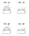
- the ink 6 applied to the openings 4 by means of an ink-jet system fills the recesses defined by the partition walls 3 and the spreading tendency of the ink 6 is suppressed by the ink-repellence of the surface of the partition walls 3 at and near the top thereof, as illustrated in FIGS. 7A and 8A.
- the ink 6 applied at an enhanced rate reduces its volume as a result of the setting steps that involve heat treatment.
- the surface of the partition walls 3 is very coarse, it contacts with ink over a large area so that, once ink 6 contacts with the lateral surface of the partition walls 3, it can easily maintain the contact regardless of the ink-repellence of the surface of the partition walls 3. Therefore, the surface of the pixels 7 can easily become flat when the ink 6 is completely set as shown in FIG. 7B.
- the surface of the partition walls 3 is flat and smooth, the surface of ink 6 falls from the initial positions to be repelled by the lateral surfaces of the partition walls 3 because of the reduction of its volume due to setting and the ink-repellence of the surfaces as shown in FIG. 8B.
- the pixels 7 show a low density along the periphery thereof in the case of a color filter and a reduction of luminance in the case of an EL element.
- the arithmetic mean deviation (Ra) of the surface of the partition walls 3 is preferably not smaller than 3nm.
- the linearity of the pattern of the partition walls 3 can be adversely affected and the openings defined by the partition walls 3 can dimensionally vary to make it difficult to have a large aperture ratio when the mean deviation (Ra) exceeds 50nm. Therefore, for the purpose of the present invention, the mean deviation (Ra) of the surface of the partition walls 3 is preferably between 3nm and 50nm, more preferably between 4nm and 20nm. Then, blank areas are prevented from appearing without adversely affecting the profile of the pattern of the partition walls 3 and the pixel surface is flattened.
- the surface coarseness of the partition walls 3 can be controlled by forming the partition walls 3 from a resin composition containing carbon black and appropriately selecting the conditions for the dry etching step and the plasma treatment step.
- the surface coarseness can vary depending on the method of plasma generation, the distance separating the electrodes, the type of gas, the RF power and the process time of the dry etching step and those of the plasma treatment process.
- a desired degree of surface coarseness can be realized by controlling the RF power and the process time.
- the surface coarseness can also vary depending on the method of plasma generation, the distance separating the electrodes, the type of gas, the RF power and the process time selected for the plasma treatment step, of which the type of gas is particularly significant.
- the surface coarseness will be more remarkable when a mixture gas of CF 4 and O 2 is used than when only CF 4 is used as gas containing fluorine atoms.
- the surface coarseness can also vary depending on the mixing ratio of O 2 gas in the mixture gas.
- the mixing ratio of O2 is preferably not greater than 30%, more preferably between 10 and 20%.
- Inks 6 of R, G and B are applied to the areas surrounded by the partition walls 3 (openings 4) of the substrate 1 from an ink-jet head 5 of an ink-jet recording system.
- An ink-jet head of the bubble jet type using electrothermal transducers as energy generating elements or of the piezo jet type using piezoelectric elements as energy generating elements may be used for the purpose of the invention.
- inks 6 contain respective coloring agents of R, G and B that produce colored sections after setting.
- inks 6 contains respective materials that produce light emitting layers adapted to emit light when a voltage is applied thereto after setting. In either case, inks 6 preferably contain at least a setting ingredient, water and a solvent.
- dye type coloring agents can be used in inks for the purpose of the invention.
- a dispersing agent may have to be added in order to disperse the pigment uniformly in ink to consequently reduce the content ratio of the coloring agent in the overall solid content.
- dye type coloring agents are preferably used for the purpose of the invention.
- the coloring agents are added at a rate equal to or less than the rate at which the setting ingredient is added, which will be described hereinafter.
- inks preferably contain one ore more than one crosslinkable monomers and/or polymers as ingredients for fixing the coloring agents by setting as a result of heat treatment or irradiation of light.
- a settable resin composition is preferable for the purpose of the invention.
- base resin materials examples include acrylic resins and silicone resins having functional groups such as hydroxy groups, carboxyl groups, alkoxy groups or amide groups; cellulose derivatives such as hydroxypropyl cellulose, hydroxyethyl cellulose, methyl cellulose carboxymethyl collulose and their modified substances; and vinyl polymers such as polyvinyl pyrrolidone, polyvinyl alcohol and polyvinyl acetal.
- a crosslinking agent and/or a photoinitiator for setting the base resin material by irradiation of light or heat treatment may also be used.
- Specific examples of crosslinking agents that can be used for the purpose of the invention include melamine derivatives such as methylolmelamine.
- photoinitiators examples include dichromates, bisazide compounds, radical type initiators, cationic initiators and anionic initiators.
- a mixture of two or more than two different photoinitiators or that of a photoinitiator and a sensitizer may also be used for the purpose of the invention.
- a mixed solvent of water and an organic solvent is preferably used as medium of inks for the purpose of the invention.
- organic solvents examples include alkyl alcohols having 1 to 4 carbon atoms such as methyl alcohol, ethyl alcohol, n-propyl alcohol, isopropyl alcohol, n-butyl alcohol, sec-butyl alcohol and tert-butyl alcohol; amides such as dimethylformamide and dimethylacetamide, ketones and keto-alcohols such as acetone, diacetone alcohol, ethers such as tetrahydrofuran and dioxane, polyalkylene glycols such as polyethylene glycol and polypropylene glycol; alkylene glycols having an aklylene group with 2 to 4 carbon atoms such as ethylene glycol, propylene glycol, butylenes glycol, triethylene glycol, thiodiglycol, hexylene glycol and diethylene glycol; glycerols; lower alkyl ethers of polyhydric alcohols such as ethylene glycol monomethyl ether,
- a mixture of two or more than two organic solvents showing different boiling points may be used in place of a single solvent and a surface active agent, a defoaming agent and/or an antiseptic agent may be added to make produce inks showing desired values for physical properties.
- a protection layer and/or a transparent electroconductive film are formed as described earlier.
- Materials that can be used for the protection layer include resin materials of the photosetting type, the thermosetting type and the photo-thermo-setting type.
- the protection layer may be made of an inorganic film prepared by evaporation or sputtering. In other words, any film that can retain the degree of transparency necessary for a color filter and withstand the transparent electroconductive film forming process and the orientation film forming process that follow.
- the transparent electroconductive film may be formed directly on the colored sections without using a protection layer interposed therebetween.
- the surface of the substrate may be subjected to a water treatment process of contacting the surface with water after the plasma treatment process of irradiating the dry etched substrate with plasma (the above described Step e) and before the process of applying the areas surrounded by the partition walls 3 (the above described Step f).
- a water treatment process of contacting the surface with water after the plasma treatment process of irradiating the dry etched substrate with plasma (the above described Step e) and before the process of applying the areas surrounded by the partition walls 3 (the above described Step f).
- Water to be used in this process is preferably pure water.
- the substrate 1 may be dipped into water or showered with water.
- the pattern on the substrate 1 shows a complex profile, preferably the substrate 1 is immersed into water and simultaneously irradiated with ultrasonic waves or is showered with water drops under slightly high pressure in order to make the boundary areas of the partition walls 3 and the openings 4, the corners and other minute areas satisfactorily contact with water.
- the temperature of water that is brought into contact with substrate 1 is preferably high from the viewpoint of improving the surface condition of the openings 4, it is preferably between 20 and 60°C in view of the cost and the economic effect of heating water.
- the effect of spreading ink can be reduced if the substrate is heated and dried at temperature higher than 100°C after the contact of the substrate 1 and water of this process. Therefore, the heating process is preferably conducted at temperature lower than 100°C.
- Black photoresist containing carbon black (“V-259BK Resist", available from Shinnittetsu Kagaku) was applied to a glass substrate (#1737, available from Corning) and subjected to predetermined processes of exposure to light, development and post baking to prepare a black matrix pattern (partition walls) having a film thickness of 2pm and oblong openings with dimensions of 75 ⁇ m x 225 ⁇ m.
- Inks of R, G and B having the compositions listed below were prepared by using a thermosetting ingredient containing acrylic copolymers shown below with their content ratios.
- Thermosetting ingredient methyl methacrylate 50 wt. parts hydroxyethyl methacrylate 30 wt. parts N-methylol-acrylamide 20 wt. parts
- R ink C. I. Acid Orange 148 3.5 wt. parts
- I. Acid Red 289 0.5 wt. parts diethylene glycol 30 wt. parts ethylene glycol 20 wt. parts ion-exchanged water 40 wt. parts the cited setting ingredient 6 wt. parts
- G ink C. I. Acid Yellow 23 2 wt.
- the glass substrate (black matrix substrate) carrying a black matrix was subjected to a dry etching process under the following conditions, using a cathode coupling - parallel plate type plasma treatment system.
- used gas O 2 gas flow rate: 80 sccm pressure: 8 Pa
- RF power 150 W treating time: 30 sec
- the black matrix substrate was subjected to a plasma treatment process in the same system under the following conditions.
- used gas CF 4 gas flow rate: 80 sccm pressure: 50 Pa
- the plasma-treated black matrix substrate was observed for the contact angles relative to pure water, using an automatic cleansing/treatment inspection apparatus for liquid crystal glass (manufactured by Kyowa Kaimen KK).
- the contact angle of the black matrix surface was measured in the 5mm wide margins around fine pattern while that of the glass substrate surface was measured outside the margins where no black matrix pattern existed.
- the measured contact angles for pure water were as follows: glass substrate surface: 6° black matrix surface: 126°
- the surface coarseness of the black matrix was observed in terms of the average coarseness (Ra) in the 5mm wide margins as in the case of the contact angle relative to pure water by means of a contact type surface coarseness meter "FP-20" (manufactured by Tecnor). As a result, the average coarseness (Ra) of the surface of the black matrix was found to be equal to 4.4nm.
- the above cited R, G and B inks were applied to the plasma-treated black matrix substrate by means of an ink-jet recording system provided with an ink-jet head having a discharge capacity of 20pl. Subsequently, the substrate was subjected to heat treatment conducted at 90°C for 10 minutes and then at 230°C for 30 minutes to thermally set the ink and produce colored sections (pixels). As a result of the heat setting process, a color filter was prepared. A total of seven specimens of color filter were prepared by changing the volume of applied ink by every 100pl within the range of 200 to 800pl per each opening in order to make them show different amount of applied ink.
- the prepared specimens of color filter were evaluated for intermingling of colors and blank areas by observing them through an optical microscope.
- the specimens carrying ink by 300pl per opening were also evaluated for flatness by means of the surface coarseness meter used for evaluating the surface coarseness.
- the difference (d t- d b ) of the height d t of the center of each colored section from the glass surface and the height d b of the edges of the colored section from the glass surface was determined and the colored section was evaluated as flat when -0.5 ⁇ m ⁇ (d t -d b ) ⁇ 0.5 ⁇ m, as recessed when (d t -d b ) ⁇ -0.5 ⁇ m and as projecting when (d t -d b ) > 0.5 ⁇ m.
- Specimens of color filter were prepared as in Example 1 except that "CK-S171X Resist" (available from Fuji Film Orin) was used for the black matrix containing carbon black. After the plasma treatment process, the black matrix substrate showed the following contact angles relative to pure water. glass substrate surface: 5 black matrix substrate surface: 128
- the average coarseness (Ra) of the surface of the black matrix was 10.3nm.
- the specimens of color filter of this example did not show any intermingling of colors nor blank areas and their colored sections showed a flat surface.
- Specimens of color filter were prepared as in Example 1 except that argon gas was introduced for the dry etching process. After the plasma treatment process, the black matrix substrate showed the following contact angles relative to pure water. glass substrate surface: 8° black matrix surface: 132°
- the average coarseness (Ra) of the surface of the black matrix was 6.8nm.
- the specimens of color filter of this example did not show any intermingling of colors nor blank areas and their colored sections showed a flat surface.
- Specimens of color filter were prepared as in Example 1 except that a mixture of CF 4 gas and O 2 gas were introduced at respective flow rates of 64sccm and 16sccm for the plasma treatment process.
- the black matrix substrate After the plasma treatment process, the black matrix substrate showed the following contact angles relative to pure water. glass substrate surface: 7° black matrix surface: 133°
- the average coarseness (Ra) of the surface of the black matrix was 5.2nm.
- the specimens of color filter of this example did not show any intermingling of colors nor blank areas and their colored sections showed a flat surface.
- Specimens of color filter were prepared as in Example 1 except that C 5 F 8 gas was introduced for the plasma treatment process. After the plasma treatment process, the black matrix substrate showed the following contact angles relative to pure water. glass substrate surface: 6° black matrix surface: 129°
- the average coarseness (Ra) of the surface of the black matrix was 3.8nm.
- the specimens of color filter of this example did not show any intermingling of colors nor blank areas and their colored sections showed a flat surface.
- Specimens of color filter were prepared as in Example 1 except that the black matrix was formed by using the same black resist as in Example 2, that the dry etching process was conducted in the same manner as in Example 3 and that the plasma treatment process was conducted in the same manner as in Example 4.
- the black matrix substrate showed the following contact angles relative to pure water. glass substrate surface: 7° black matrix surface: 134°
- the average coarseness (Ra) of the surface of the black matrix was 18.3nm.
- the specimens of color filter of this example did not show any intermingling of colors nor blank areas and their colored sections showed a flat surface.
- Example 1 Specimens of color filter were prepared as in Example 1 except that the black resist of Example 1 was replaced by "CT-2000L" (available from Fuji Film Orin) that is transparent photosensitive resin containing no carbon black.
- CT-2000L available from Fuji Film Orin
- the matrix pattern substrate showed the following contact angles relative to pure water. glass substrate surface: 6° matrix pattern surface: 102°
- the average coarseness (Ra) of the surface of the matrix pattern was 1.5nm.
- Specimens of color filter were prepared as in Example 1 except that neither the dry etching process nor the plasma treatment process was conducted.
- the obtained black matrix substrate showed the following contact angles relative to pure water.
- the average coarseness (Ra) of the surface of the black matrix was 2.0nm.
- the specimens of color filter prepared in this comparative example showed blank areas in all the colored sections thereof. Intermingling of colors was observed in the specimens carrying ink by 400pl or more per opening. It was not possible to evaluate the flatness of the surface of the colored sections because of the blank areas.
- Specimens of color filter were prepared as in Example 1 except that no dry etching process was conducted. After the plasma treatment process, the obtained black matrix showed the following contact angles relative to pure water. glass substrate surface: 23° black matrix surface: 97°
- the average coarseness (Ra) of the surface of the black matrix was 3.5nm.
- the specimens of color filter prepared in this comparative example showed no blank areas and the surface of their colored sections was flat. Intermingling of colors was however observed in the specimens carrying ink by 600pl or more per opening.
- Table 1 summarily shows the results of the above examples and comparative examples.
- a TFT drive substrate comprising a multiplayer structure of wiring films and insulating films formed by way of a thin film process was brought in. Then, an ITO film was formed by means of sputtering on the TFT drive substrate to a thickness of 40nm as transparent electrode for each pixel (light emitting layer) and subjected to a patterning operation by means of photolithography to produce pixels showing a predetermined profile.
- Transparent photosensitive resin "CT-2000L” available from Fuji Film Orin
- CT-2000L Transparent photosensitive resin
- the substrate was subjected to a dry etching process using O 2 and a plasma treatment process using CF 4 under the conditions same as those used in Example 1.
- the surface of the ITO transparent electrodes and the transparent matrix pattern respectively showed the following contact angles relative to pure water.
- the spaces defined by the partition walls on the substrate were filled with the light emitting layer.
- electron-transporting 2,5-bis(5-tert-butyl-2-benzoxazolyl)-thiophene fluorescence peak: 450nm, a light emitting center forming compound that operates as an electron-transporting blue light emitting coloring matter, to be referred to as "BBOT” hereinafter
- BBOT light emitting center forming compound that operates as an electron-transporting blue light emitting coloring matter
- the dichloroethane solution of PVK-BBOT that additionally contained Nile Red by 0.015 mol% as another light emitting center forming compound was filled in the spaces defined by the partition walls of transparent resin by means of an ink-jet system and then dried to produce 200nm thick light emitting layers.
- the pixels (light emitting layers) were isolated from each other and the solution containing said light emitting materials did not move beyond the partition walls.
- an Mg:Ag cathode was formed to a thickness of 200nm by means of vacuum evaporation of Mg:Ag (10:1).
- a voltage of 18V was applied to each of the pixels of the prepared EL element to prove that the element emitted white light uniformly at a rate of 480 cd/m 2 .
- Black photoresist containing carbon black (“CK-S171 Resist” (available from Fuji Film Orin) was applied to a glass substrate (#1737, available from Corning) and subjected to predetermined processes of exposure to light, development and post baking to prepare a black matrix pattern (partition walls) having a film thickness of 2pm and oblong openings with dimensions of 75 ⁇ m x 225 ⁇ m.
- the surface coarseness of the glass substrate used for forming the black matrix thereon was observed at selected positions by means of "NanoScope IIIa AFM Dimension 3000 Stage System” (manufactured by Digital Instrument). As a result, the average coarseness (Ra) of the surface of the black matrix was found to be equal to 0.231nm.
- the glass substrate (black matrix substrate) carrying a black matrix was subjected to plasma treatment under the conditions same as those of Example 1.
- the black matrix substrate was subjected to a plasma treatment process in the same system under the conditions same as those of Example 1.
- the plasma-treated black matrix substrate was observed for the contact angles relative to pure water as in Example 1.
- the contact angles relative to pure water were as follows. glass substrate surface: 6° black matrix surface: 126°
- the surface coarseness of the black matrix was observed as in Example 1.
- the average coarseness (Ra) of the surface of the black matrix was found to be equal to 4.4nm.
- the surface coarseness of the glass substrate was also evaluated after the plasma treatment to find that the average coarseness (Ra) of the surface of the glass substrate was 0.222nm.
- the black matrix substrate was evaluated for the ink spreading performance.
- the above-described B ink was applied to the each of the openings of the micro-pattern by 20pl from an ink-jet head and the black matrix was observed through an optical microscope to find that the ink droplets showed a diameter of 50 ⁇ m.
- the applied ink was left on the substrate for a while to find that the droplets did not wet the surrounding walls nor spread around.
- the black matrix substrate was subjected to water treatment. More specifically, the black matrix substrate was immersed in an ultrasonic pure water bath under the following treatment conditions. Pure water temperature: 30°C ultrasonic wave frequency: 40 kHz treating time: 2 min drying temperature: 90°C drying time: 2 min.
- the ink-repellence of the surface of the black matrix substrate was observed again to see if it had not been damaged by the water treatment by observing the contact angles relative to pure water at the positions same as those observed prior to the water treatment.
- the contact angles relative to pure water were as follows. glass substrate surface: 7° black matrix surface: 124°
- the black matrix substrate was evaluated for the ink spreading performance, using the method same as the one used prior to the water treatment.
- the black matrix - substrate was observed for the diameter of ink droplets through an optical microscope to find that the ink droplets had thoroughly wetted the surrounding walls and spread fully in the respective openings so that the boundary of each droplet was hardly recognizable.
- the average coarseness (Ra) of the surface of the glass substrate was 0.794nm.
- the change in the amount of the fluorine compound on the surface of the glass substrate was observed by means of "TFS-2000" (manufactured by TOF-SIMS PHI EVANS) at three positions including (1) a position on the surface of the glass substrate before forming the black matrix, (2) a position on the area of the surface of the glass substrate outside the margins of the black matrix where no black matrix pattern was found after the plasma treatment and (3) a position on the surface of the glass substrate outside the margins of the black matrix where no black matrix pattern was found after the water treatment.
- the change in the fluorine compound was evaluated by way of Si+ normalization (i.e., assuming that the value of Si+ was 100).
- Si+ normalized values of CaF+, SrF+ and BaF+ at position (2) were 161.7, 69.0 and 102.3, respectively, while all those values at positions (1) and (3) were below 1.
- Si+ normalized value of CF 3 + at position (2) was 42.2 while those values at positions (1) and (3) were below 1.
- the amount of the fluorine compound on the surface of the glass substrate after the water treatment was 0.052% in term of the ratio of the Si+ normalized value for BaF+ if compared with the value before the water treatment.
- the above cited R, G and B inks were applied to the water-treated black matrix substrate by means of an ink-jet recording system provided with an ink-jet head having a discharge capacity of 20pl until each opening was made to carry 40pl of ink. Subsequently, the substrate was subjected to heat treatment conducted at 90°C for 10 minutes and then at 230°C for 30 minutes to thermally set the ink and produce colored sections (pixels).
- the prepared specimens of color filter were evaluated for blank areas by observing them through an optical microscope.
- the specimens carrying ink by 40p1 per opening were also evaluated for flatness by means of the surface coarseness meter used for evaluating the surface coarseness. More specifically, the difference (d t -d b ) of the height d t of the center of each colored section from the glass surface and the height d b of the edges of the colored section from the glass surface was determined and the colored section was evaluated as flat when -0.5 ⁇ m ⁇ (d t -d b ) ⁇ 0.5 ⁇ m, as recessed when (d t -d b ) ⁇ -0.5 ⁇ m and as projecting when (d t -d b ) > 0.5 ⁇ m.
- Specimens of color filter were prepared as in Example 9 except that "V-259BKIS Resist” (available from Shinnittetsu Kagaku) was used as black resist containing carbon black. After the water treatment process, the black matrix substrate showed the following contact angles relative to pure water. glass substrate surface: 5° black matrix surface: 128°
- the ink spreading performance was also evaluated to find that the 20pl of ink had satisfactorily wetted the inside of each opening and spread around.
- the average coarseness (Ra) of the surface of the black matrix was 10.3nm and that of the surface of the glass substrate was 0.743nm.
- the amount of the fluorine compound on the surface of the glass substrate after the water treatment was 0.042% in term of the ratio of the Si+ normalized value for BaF+ if compared with the value before the water treatment.
- the specimens of color filter of this example did not show any blank areas and their colored sections showed a flat surface.
- Specimens of color filter were prepared as in Example 9 except that a mixture of CF 4 gas and O 2 gas were introduced at respective flow rates of 64sccm and 16sccm for the plasma treatment process.
- the black matrix substrate After the water treatment process, the black matrix substrate showed the following contact angles relative to pure water.
- the average coarseness (Ra) of the surface of the glass substrate prior to the water treatment was 0.217nm.
- the ink spreading performance was also evaluated to find that the 20pl of ink had satisfactorily wetted the inside of each opening and spread around.
- the average coarseness (Ra) of the surface of the black matrix was 5.2nm and that of the surface of the glass substrate was 0.761nm.
- the amount of the fluorine compound on the surface of the glass substrate after the water treatment was 0.048% in term of the ratio of the Si+ normalized value for BaF+ if compared with the value before the water treatment.
- the specimens of color filter of this example did not show any blank areas and their colored sections showed a flat surface.
- Example 9 Specimens of color filter were prepared as in Example 9 except that the black resist of Example 9 was replaced by "CT-2000L" (available from Fuji Film Orin) that is transparent photosensitive resin containing no carbon black.
- CT-2000L available from Fuji Film Orin
- the matrix pattern substrate showed the following contact angles relative to pure water. glass substrate surface: 6° matrix pattern surface: 62°
- the ink spreading performance was also evaluated to find that the 20pl of ink had satisfactorily wetted the inside of each opening and spread around.
- the average coarseness (Ra) of the surface of the matrix pattern was 1.5nm and that of the surface of the glass substrate was 0.787nm.
- the amount of the fluorine compound on the surface of the glass substrate after the water treatment was 0.045% in term of the ratio of the Si+ normalized value for BaF+ if compared with the value before the water treatment.
- the specimens of color filter of this example did not show any blank areas and their colored sections were projecting only slightly and the boundaries of the colored sections and the matrix pattern showed a slightly low density only to such an extent that no problem arises therefrom in practical applications.
- Specimens of color filter were prepared as in Example 9 except that the temperature of pure water used for the water treatment was held to 50°C and the treating time was made to be equal to 30 sec. After the water treatment process, the black matrix substrate showed the following contact angles relative to pure water. glass substrate surface: 8° black matrix surface: 124°
- the ink spreading performance was also evaluated to find that the 20pl of ink had satisfactorily wetted the inside of each opening and spread around.
- the average coarseness (Ra) of the surface of the black matrix was 10.5nm and that of the surface of the glass substrate was 0.753nm.
- the amount of the fluorine compound on the surface of the glass substrate after the water treatment was 0.041% in term of the ratio of the Si+ normalized value for BaF+ if compared with the value before the water treatment.
- the specimens of color filter of this example did not show any blank areas and their colored sections showed a flat surface.
- Specimens of color filter were prepared as in Example 9 except that the plasma-treated substrate was subjected to water treatment using a pure water shower cleaning system. The showering time was 30 sec and the pure water temperature was 35°C. The drying conditions of Example 9 were also used here. After the water treatment process, the black matrix substrate showed the following contact angles relative to pure water. glass substrate surface: 7° black matrix surface: 126°
- the ink spreading performance was also evaluated to find that the 20pl of ink had satisfactorily wetted the inside of each opening and spread around.
- the average coarseness (Ra) of the surface of the black matrix was 12.3nm and that of the surface of the glass substrate was 0.771nm.
- the amount of the fluorine compound on the surface of the glass substrate after the water treatment was 0.045% in term of the ratio of the Si+ normalized value for BaF+ if compared with the value before the water treatment.
- the specimens of color filter of this example did not show any blank areas and their colored sections showed a flat surface.
- Example 9 Specimens of color filter were prepared as in Example 9 except that the plasma-treated substrate was subjected to water treatment using a high pressure spray cleaning system. Pure water was used for the high pressure spraying. The spraying pressure was selected to be 6.86 ⁇ 10 6 N/m 2 (70 kgf/cm 2 ). The drying conditions of Example 9 were also used here. After the water treatment process, the black matrix substrate showed the following contact angles relative to pure water. glass substrate surface: 5° black matrix surface: 124°
- the ink spreading performance was also evaluated to find that the 20pl of ink had satisfactorily wetted the inside of each opening and spread around.
- the average coarseness (Ra) of the surface of the black matrix was 9.9nm and that of the surface of the glass substrate was 0.748nm.
- the amount of the fluorine compound on the surface of the glass substrate after the water treatment was 0.044% in term of the ratio of the Si+ normalized value for BaF+ if compared with the value before the water treatment.
- the specimens of color filter of this example did not show any blank areas and their colored sections showed a flat surface.
- a TFT drive substrate comprising a multiplayer structure of wiring films and insulating films formed by way of a thin film process was brought in. Then, an ITO film was formed by means of sputtering on the TFT drive substrate to a thickness of 40nm as transparent electrode for each pixel (light emitting layer) and subjected to a patterning operation by means of photolithography to produce pixels showing a predetermined profile.
- the average coarseness (Ra) was found to be equal to 31.5nm. Then, the substrate was subjected to a water treatment process. The surface of the ITO transparent electrodes and the transparent matrix pattern respectively showed the following contact angles relative to pure water after the water treatment process.
- Ink was applied to the inside of the openings defined by the partition walls by means of an ink-jet recording system.
- electron-transporting 2,5-bis(5-tert-butyl-2-benzoxazolyl)-thiophene fluorescence peak: 450nm, a light emitting center forming compound that operates as an electron-transporting blue light emitting coloring matter, to be referred to as "BBOT” hereinafter
- BBOT a light emitting center forming compound that operates as an electron-transporting blue light emitting coloring matter
- the dichloroethane solution of PVK-BBOT that additionally contained Nile Red by 0.015 mol% as another dissolved light emitting center forming compound was filled in the spaces defined by the partition walls of transparent resin by means of an ink-jet system and then dried to produce 200nm thick light emitting layers.
- the pixels (light emitting layers) were isolated from each other and the solution containing said light emitting materials did not move beyond the partition walls.
- an Mg:Ag cathode was formed to a thickness of 200nm by means of vacuum evaporation of Mg:Ag (10:1). A voltage of 18V was applied to each of the pixels of the prepared EL element to prove that the element emitted white light uniformly at a rate of 480 cd/m 2 .
- an optical element such as a color filter or an EL element comprising pixels that are free from the problems of intermingling of colors, blank areas and uneven density in the colored sections in a simple process at low cost so that the method can provide reliable optical elements at a high manufacturing yield. Therefore, it is now possible to provide a liquid crystal element adapted to display excellent color images and comprising optical filters produced by the manufacturing method according to the invention at low cost.
Landscapes
- Physics & Mathematics (AREA)
- Nonlinear Science (AREA)
- General Physics & Mathematics (AREA)
- Optics & Photonics (AREA)
- Mathematical Physics (AREA)
- Chemical & Material Sciences (AREA)
- Crystallography & Structural Chemistry (AREA)
- Optical Filters (AREA)
- Electroluminescent Light Sources (AREA)
- Glass Compositions (AREA)
- Optical Integrated Circuits (AREA)
Claims (10)
- Procédé de fabrication d'un élément optique comprenant au moins une pluralité de pixels formés sur un substrat et des parois de séparation disposées respectivement entre des pixels adjacents, ledit procédé comprenant les étapes consistant à :former des parois de séparation d'une composition de résine sur un substrat,exécuter un processus de gravure à sec consistant à faire rayonner sur le substrat, portant lesdites parois de séparation formées sur celui-ci, un plasma dans une atmosphère contenant un gaz sélectionné au moins parmi l'oxygène, l'argon et l'hélium,exécuter un processus de traitement au plasma consistant à faire rayonner sur le substrat, soumis audit processus de gravure à sec, un plasma dans une atmosphère contenant au moins des atomes de fluor, etformer des pixels en appliquant une encre aux zones entourées par les parois de séparation au moyen d'un système à jet d'encre,caractérisé en ce que
lesdites parois de séparation sont formées à partir d'une composition de résine contenant du noir de carbone et l'angle de contact de la surface des parois de séparation relatif à l'eau pure n'est pas inférieur à 110°. - Procédé selon la revendication 1, dans lequel ledit angle de contact n'est pas inférieur à 120° et n'est pas supérieur à 135°.
- Procédé de fabrication d'un élément optique selon la revendication 1 ou 2, dans lequel les conditions de gravure à sec et de traitement au plasma sont choisies de manière à ce que l'écart moyen arithmétique (Ra) de la surface des parois de séparation après ledit traitement au plasma soit entre 3 nm et 50 nm.
- Procédé de fabrication d'un élément optique selon l'une quelconque des revendications 1 à 3, dans lequel l'angle de contact de la surface du substrat relatif à l'eau pure n'est pas supérieur à 20° après ledit processus de traitement au plasma.
- Procédé selon l'une quelconque des revendications 1 à 4, dans lequel le gaz introduit dans ledit processus de traitement au plasma est au moins un gaz d'un halogène choisi à partir de CF4, SF6, CHF3, C2F6, C3F8 et C5F8.
- Procédé selon l'une quelconque des revendications 1 à 4, dans lequel le gaz introduit dans ledit processus de traitement au plasma est au moins un mélange d'un gaz d'halogène sélectionné à partir de CF4, SF6, CHF3, C2F6, C3F8 et C5F8 et d'un gaz de O2 et le rapport de mélange du gaz de O2 n'est pas supérieur à 30 %.
- Procédé selon l'une quelconque des revendications 1 à 6, dans lequel ladite encre contient au moins un ingrédient de durcissement, de l'eau et un solvant organique.
- Procédé selon l'une quelconque des revendications 1 à 7, dans lequel, après ledit processus de traitement au plasma destiné à faire rayonner un plasma sur ledit substrat gravé à sec, le substrat traité au plasma est soumis à un processus de traitement à l'eau.
- Procédé selon l'une quelconque des revendications 1 à 8, dans lequel est conçu pour fabriquer un filtre de couleur où ledit substrat est un substrat transparent et lesdites parois de séparation sont procurées par une matrice noire.
- Procédé selon l'une quelconque des revendications 1 à 8, conçu pour fabriquer un élément à électroluminescence, où lesdits pixels sont formés par une couche d'émission de lumière et ledit élément à électroluminescence comprend une paire d'électrodes prenant en sandwich ladite couche d'émission de lumière.
Applications Claiming Priority (4)
| Application Number | Priority Date | Filing Date | Title |
|---|---|---|---|
| JP2000165584 | 2000-06-02 | ||
| JP2000165584A JP3854782B2 (ja) | 2000-06-02 | 2000-06-02 | 光学素子とその製造方法 |
| JP2000311411A JP4677085B2 (ja) | 2000-10-12 | 2000-10-12 | 光学素子の製造方法 |
| JP2000311411 | 2000-10-12 |
Publications (3)
| Publication Number | Publication Date |
|---|---|
| EP1160590A2 EP1160590A2 (fr) | 2001-12-05 |
| EP1160590A3 EP1160590A3 (fr) | 2004-06-09 |
| EP1160590B1 true EP1160590B1 (fr) | 2006-04-26 |
Family
ID=26593204
Family Applications (1)
| Application Number | Title | Priority Date | Filing Date |
|---|---|---|---|
| EP01113276A Expired - Lifetime EP1160590B1 (fr) | 2000-06-02 | 2001-05-31 | Méthode de fabrication d'un élement optique |
Country Status (7)
| Country | Link |
|---|---|
| US (2) | US6677243B2 (fr) |
| EP (1) | EP1160590B1 (fr) |
| KR (1) | KR100424030B1 (fr) |
| CN (2) | CN100406994C (fr) |
| AT (1) | ATE324603T1 (fr) |
| DE (1) | DE60119025T8 (fr) |
| TW (1) | TW514592B (fr) |
Families Citing this family (65)
| Publication number | Priority date | Publication date | Assignee | Title |
|---|---|---|---|---|
| GB9713074D0 (en) * | 1997-06-21 | 1997-08-27 | Cambridge Display Tech Ltd | Electrically-conducting colour filters for use in organic light-emitting displays |
| ATE324603T1 (de) * | 2000-06-02 | 2006-05-15 | Canon Kk | Herstellungsverfahren für ein optisches element |
| JP2003084123A (ja) * | 2001-06-29 | 2003-03-19 | Seiko Epson Corp | カラーフィルタ基板、カラーフィルタ基板の製造方法、液晶表示装置、電気光学装置、電気光学装置の製造方法及び電子機器 |
| US6810919B2 (en) | 2002-01-11 | 2004-11-02 | Seiko Epson Corporation | Manufacturing method for display device, display device, manufacturing method for electronic apparatus, and electronic apparatus |
| KR100786835B1 (ko) * | 2002-01-21 | 2007-12-20 | 삼성에스디아이 주식회사 | 액정 표시 소자와 이의 제조 방법 |
| KR20020025918A (ko) * | 2002-02-15 | 2002-04-04 | 박병주 | 습식 공정으로 제작된 유기 반도체 디바이스 및 유기전계발광 소자 |
| JP2003237060A (ja) * | 2002-02-20 | 2003-08-26 | Seiko Epson Corp | デバイスの製造装置及び製造方法、デバイスの製造装置の駆動方法 |
| JP3838964B2 (ja) | 2002-03-13 | 2006-10-25 | 株式会社リコー | 機能性素子基板の製造装置 |
| JP2003273111A (ja) * | 2002-03-14 | 2003-09-26 | Seiko Epson Corp | 成膜方法及びその方法を用いて製造したデバイス、並びにデバイスの製造方法 |
| DE10236404B4 (de) * | 2002-08-02 | 2008-01-10 | Samsung SDI Co., Ltd., Suwon | Verfahren zur Herstellung eines Substrates |
| JP4165692B2 (ja) * | 2002-08-05 | 2008-10-15 | 大日本印刷株式会社 | エレクトロルミネッセント素子の製造方法 |
| KR100542740B1 (ko) * | 2002-11-11 | 2006-01-11 | 삼성전자주식회사 | 가스 플라즈마 생성 방법 및 장치, 플라즈마 생성용 가스조성물 및 이를 이용한 반도체 장치의 제조 방법 |
| DE10310524A1 (de) * | 2003-03-11 | 2004-09-23 | Micronas Gmbh | Verfahren zum Ätzen einer Probe sowie Ätzanlage |
| JP4628109B2 (ja) * | 2003-04-25 | 2011-02-09 | 株式会社半導体エネルギー研究所 | 半導体装置の作製方法 |
| JP2004363560A (ja) * | 2003-05-09 | 2004-12-24 | Seiko Epson Corp | 基板、デバイス、デバイス製造方法、アクティブマトリクス基板の製造方法及び電気光学装置並びに電子機器 |
| DE10343351B4 (de) * | 2003-09-12 | 2017-01-05 | Samsung Display Co., Ltd. | Substrat zum Tintenstrahldrucken und Verfahren zu dessen Herstellung |
| US7833612B2 (en) | 2003-09-12 | 2010-11-16 | Samsung Mobile Display Co., Ltd. | Substrate for inkjet printing and method of manufacturing the same |
| US20050069713A1 (en) * | 2003-09-30 | 2005-03-31 | Rahul Gupta | Capillary coating method |
| CN100568457C (zh) * | 2003-10-02 | 2009-12-09 | 株式会社半导体能源研究所 | 半导体装置的制造方法 |
| US20050153114A1 (en) * | 2004-01-14 | 2005-07-14 | Rahul Gupta | Printing of organic electronic devices |
| US20050170643A1 (en) * | 2004-01-29 | 2005-08-04 | Semiconductor Energy Laboratory Co., Ltd. | Forming method of contact hole, and manufacturing method of semiconductor device, liquid crystal display device and EL display device |
| GB0402559D0 (en) * | 2004-02-05 | 2004-03-10 | Cambridge Display Tech Ltd | Molecular electronic device fabrication methods and structures |
| US7416977B2 (en) * | 2004-04-28 | 2008-08-26 | Semiconductor Energy Laboratory Co., Ltd. | Method for manufacturing display device, liquid crystal television, and EL television |
| JP4464210B2 (ja) * | 2004-06-29 | 2010-05-19 | 東北パイオニア株式会社 | 有機elパネルの形成方法 |
| JP4175298B2 (ja) * | 2004-07-07 | 2008-11-05 | セイコーエプソン株式会社 | カラーフィルタとその製造方法及び電気光学装置並びに電子機器 |
| JP2006098555A (ja) * | 2004-09-28 | 2006-04-13 | Dainippon Printing Co Ltd | カラーフィルタおよびその製造方法 |
| US20060084276A1 (en) * | 2004-10-14 | 2006-04-20 | Janet Yu | Methods for surface treatment and structure formed therefrom |
| US20060108905A1 (en) | 2004-11-25 | 2006-05-25 | Samsung Electronics Co., Ltd. | Mold for fabricating barrier rib and method of fabricating two-layered barrier rib using same |
| US8334012B2 (en) * | 2004-12-20 | 2012-12-18 | Palo Alto Research Center Incorporated | Method for preprinting and/or reliquifying subpixels to achieve color uniformity in color filters |
| CN100439980C (zh) * | 2005-01-07 | 2008-12-03 | 财团法人工业技术研究院 | 彩色胆固醇型液晶显示器及其制造方法 |
| KR100903101B1 (ko) * | 2005-02-07 | 2009-06-16 | 삼성모바일디스플레이주식회사 | 유기전계 발광표시장치 및 그의 제조방법 |
| TWI345082B (en) * | 2005-03-18 | 2011-07-11 | Hon Hai Prec Ind Co Ltd | Method for manufacturing color filter |
| KR20060117034A (ko) * | 2005-05-12 | 2006-11-16 | 삼성전자주식회사 | 표시장치 및 이의 제조 방법 |
| CN100405092C (zh) * | 2005-06-17 | 2008-07-23 | 虹创科技股份有限公司 | 彩色滤光片和其制备方法 |
| JP4752349B2 (ja) | 2005-06-23 | 2011-08-17 | 大日本印刷株式会社 | パターン形成体およびその製造方法 |
| CN100565308C (zh) * | 2005-07-04 | 2009-12-02 | 财团法人工业技术研究院 | 模块化显示元件及其制造方法 |
| US7371487B2 (en) * | 2005-11-25 | 2008-05-13 | Samsung Electronics Co., Ltd. | Method of fabricating black matrix of a color filter |
| KR101326575B1 (ko) * | 2005-12-30 | 2013-11-08 | 엘지디스플레이 주식회사 | 액정표시장치의 컬러필터 제조방법 |
| JP2007194113A (ja) * | 2006-01-20 | 2007-08-02 | Hitachi Displays Ltd | 電子装置の製造方法 |
| US20070184363A1 (en) * | 2006-02-04 | 2007-08-09 | Kim Sung-Woong | Method of manufacturing a black matrix of color filter |
| CN101038351B (zh) * | 2006-03-17 | 2011-03-02 | 奇美电子股份有限公司 | 彩色滤光片基板的返工方法 |
| US7736936B2 (en) * | 2006-08-29 | 2010-06-15 | Semiconductor Energy Laboratory Co., Ltd. | Method of forming display device that includes removing mask to form opening in insulating film |
| TWI345802B (en) * | 2006-10-25 | 2011-07-21 | Ind Tech Res Inst | Methods for repairing patterned structure of electronic devices |
| US7768598B2 (en) * | 2007-03-06 | 2010-08-03 | Toppan Printing Co., Ltd. | Substrate having pattern, color filter, liquid crystal display and method of manufacturing color filter |
| JP4479737B2 (ja) * | 2007-03-07 | 2010-06-09 | セイコーエプソン株式会社 | 発光装置およびその製造方法ならびに電子機器 |
| KR101037782B1 (ko) * | 2007-04-05 | 2011-05-27 | 주식회사 엘지화학 | 컬러필터의 제조방법 및 이에 의해 제조된 컬러필터 |
| JP4576412B2 (ja) * | 2007-09-05 | 2010-11-10 | シャープ株式会社 | 着色マイクロレンズアレイの製造方法、カラー固体撮像素子およびその製造方法、カラー表示装置の製造方法、電子情報機器の製造方法 |
| JP4596287B2 (ja) * | 2008-09-19 | 2010-12-08 | カシオ計算機株式会社 | シリコンを含む膜のドライエッチング方法 |
| KR101112064B1 (ko) * | 2009-07-27 | 2012-02-13 | 엘지디스플레이 주식회사 | 액정표시장치용 컬러필터 기판의 제조방법 |
| US8576360B2 (en) * | 2009-09-09 | 2013-11-05 | Sharp Kabushiki Kaisha | Color filter substrate, liquid crystal display panel, and liquid crystal display device |
| US8336783B2 (en) * | 2010-04-19 | 2012-12-25 | George Monemvasitis | Polymeric thread with miniature pattern and fluorescent taggant for anti-counterfeit applications and method of making same |
| KR101826069B1 (ko) | 2010-10-26 | 2018-03-23 | 삼성디스플레이 주식회사 | 유기발광표시장치 및 그 제조방법 |
| KR20120089505A (ko) * | 2010-12-10 | 2012-08-13 | 삼성전자주식회사 | 표시 장치 및 그 제조 방법 |
| US9535315B2 (en) | 2011-10-31 | 2017-01-03 | Applied Materials, Inc. | Method of fabricating a color filter array using a multilevel structure |
| CN109298601A (zh) * | 2012-09-18 | 2019-02-01 | 旭化成株式会社 | 感光性树脂组合物 |
| KR20140090275A (ko) * | 2012-11-21 | 2014-07-17 | 삼성전자주식회사 | 잉크젯 프린팅 기법을 이용한 도전성 패턴 형성 방법 |
| JP6314983B2 (ja) * | 2013-06-27 | 2018-04-25 | 三菱ケミカル株式会社 | 偏光素子、及び偏光素子の製造方法 |
| CN105980624B (zh) * | 2013-12-13 | 2018-09-25 | 北面服饰公司 | 用于纺织品的着色的等离子体处理 |
| JP2016045236A (ja) * | 2014-08-20 | 2016-04-04 | Jsr株式会社 | 着色組成物、着色硬化膜及び表示素子 |
| JP6575239B2 (ja) | 2015-09-02 | 2019-09-18 | セイコーエプソン株式会社 | 機能素子の製造方法 |
| CN107634071B (zh) | 2017-10-17 | 2020-05-26 | 京东方科技集团股份有限公司 | 显示基板母板及其制作方法、显示基板、显示装置 |
| CN108205220A (zh) * | 2018-01-16 | 2018-06-26 | 青岛海信电器股份有限公司 | 黑矩阵基板及其制备方法、彩色滤光片、显示面板及设备 |
| CN111816777A (zh) * | 2019-04-11 | 2020-10-23 | 陕西坤同半导体科技有限公司 | 一种oled发光器件及其制作方法 |
| CN114333567B (zh) * | 2020-09-30 | 2023-12-08 | 京东方科技集团股份有限公司 | 黑矩阵结构及其制造方法、显示基板、显示装置 |
| CN116679471A (zh) * | 2023-05-26 | 2023-09-01 | 福耀玻璃工业集团股份有限公司 | 分区调节透光组件和车辆 |
Family Cites Families (40)
| Publication number | Priority date | Publication date | Assignee | Title |
|---|---|---|---|---|
| US4356429A (en) | 1980-07-17 | 1982-10-26 | Eastman Kodak Company | Organic electroluminescent cell |
| JPS5975205A (ja) | 1982-10-25 | 1984-04-27 | Seiko Epson Corp | カラ−フイルタの製造方法 |
| US4539507A (en) | 1983-03-25 | 1985-09-03 | Eastman Kodak Company | Organic electroluminescent devices having improved power conversion efficiencies |
| US5015856A (en) * | 1990-03-28 | 1991-05-14 | E. I. Du Pont De Nemours And Company | Automated process for permeability determinations of barrier resins |
| JPH04123005A (ja) | 1990-09-14 | 1992-04-23 | Toray Ind Inc | カラーフィルタ製造法 |
| JPH05241012A (ja) | 1992-02-26 | 1993-09-21 | Toray Ind Inc | 液晶表示用カラ−フィルタの製造方法 |
| JPH05241011A (ja) | 1992-03-02 | 1993-09-21 | Toray Ind Inc | 液晶表示用カラ−フィルタの製造方法 |
| JP3412857B2 (ja) * | 1992-05-13 | 2003-06-03 | キヤノン株式会社 | インク、画像形成方法、インクジェット記録方法、インクジェット記録ユニット、インクカートリッジおよびインクジェット記録装置 |
| JPH06244392A (ja) * | 1993-02-17 | 1994-09-02 | Sharp Corp | 固体撮像装置およびその製造方法 |
| TW417034B (en) | 1993-11-24 | 2001-01-01 | Canon Kk | Color filter, method for manufacturing it, and liquid crystal panel |
| JP3332515B2 (ja) | 1993-11-24 | 2002-10-07 | キヤノン株式会社 | カラーフィルタ、その製造方法及び液晶パネル |
| DE69523351T2 (de) | 1994-01-28 | 2002-05-02 | Canon K.K., Tokio/Tokyo | Farbfilter, Verfahren zu seiner Herstellung, und Flüssigkristalltafel |
| JP3014923B2 (ja) | 1994-06-24 | 2000-02-28 | キヤノン株式会社 | カラーフィルターおよびその製造方法ならびにそのフィルターを用いた液晶表示装置 |
| JP3190219B2 (ja) * | 1994-12-15 | 2001-07-23 | キヤノン株式会社 | 液晶用カラーフィルターの製造方法及び液晶用カラーフィルター及び該カラーフィルターを具備する液晶パネル |
| JP3576627B2 (ja) | 1995-01-25 | 2004-10-13 | キヤノン株式会社 | カラーフィルタの製造方法及び液晶表示装置 |
| US6039437A (en) * | 1995-01-31 | 2000-03-21 | Canon Kabushiki Kaisha | Ink-jet head and ink-jet printing apparatus incorporating the same |
| JP3143591B2 (ja) | 1995-09-14 | 2001-03-07 | キヤノン株式会社 | 表示装置 |
| JP3305212B2 (ja) | 1995-11-09 | 2002-07-22 | キヤノン株式会社 | 液晶素子用の基板、液晶素子、およびそれらの製造方法 |
| JPH09230129A (ja) | 1996-02-26 | 1997-09-05 | Asahi Glass Co Ltd | カラーフィルタの製造方法及びそれを用いた液晶表示素子 |
| JP3841487B2 (ja) * | 1996-07-16 | 2006-11-01 | 日本無機株式会社 | ラシヒリングとその製造方法 |
| JP3927654B2 (ja) | 1996-08-07 | 2007-06-13 | キヤノン株式会社 | カラーフィルタおよび液晶表示装置の製造方法 |
| JP3996979B2 (ja) * | 1996-08-08 | 2007-10-24 | キヤノン株式会社 | カラーフィルターの製造方法、カラーフィルター及び液晶表示装置 |
| JPH10104417A (ja) * | 1996-09-30 | 1998-04-24 | Canon Inc | カラーフィルター、これを用いた液晶素子、及びこれらの製造方法、該製造方法に用いられるインクジェット用インク |
| US5888679A (en) | 1997-03-27 | 1999-03-30 | Canon Kabushiki Kaisha | Production process of color filter, color filter produced thereby and liquid crystal display device using such color filter |
| JPH10288707A (ja) | 1997-04-15 | 1998-10-27 | Toppan Printing Co Ltd | ブラックマトリックス及びそれを用いたカラーフィルタ及びそれらの製造方法 |
| JPH10332925A (ja) | 1997-06-02 | 1998-12-18 | Canon Inc | カラーフィルタ基板とその製造方法、該基板を用いた液晶素子 |
| JPH112716A (ja) * | 1997-06-13 | 1999-01-06 | Canon Inc | カラーフィルタ、これを用いた液晶素子及びこれらの製造方法、並びに該製造方法に用いられるインクジェット用インク |
| US5891014A (en) | 1997-07-18 | 1999-04-06 | Fuji Photo Optical Co., Ltd. | Passage structure in endoscope and adapter used when washing passages in endoscope |
| JP3424896B2 (ja) | 1997-07-18 | 2003-07-07 | 富士写真光機株式会社 | 内視鏡の管路取付け構造 |
| US6195147B1 (en) | 1997-08-01 | 2001-02-27 | Canon Kabushiki Kaisha | Liquid crystal substrate with optical modulation region having different alignment control forces |
| WO1999048339A1 (fr) * | 1998-03-17 | 1999-09-23 | Seiko Epson Corporation | Substrat de formation de motifs sur film mince et son traitement de surface |
| JP3646510B2 (ja) | 1998-03-18 | 2005-05-11 | セイコーエプソン株式会社 | 薄膜形成方法、表示装置およびカラーフィルタ |
| JP2000018771A (ja) | 1998-07-03 | 2000-01-18 | Daikin Ind Ltd | 空気調和機の凝縮器の補助冷却装置 |
| JP2000035511A (ja) | 1998-07-16 | 2000-02-02 | Asahi Glass Co Ltd | カラーフィルタの製造方法及びそれを用いた液晶表示素子 |
| US6183917B1 (en) | 1998-07-31 | 2001-02-06 | Canon Kabushiki Kaisha | Color filter, production process of color filter, liquid crystal display device using the color filter, and production process of black matrix |
| KR100565738B1 (ko) * | 1999-01-29 | 2006-03-29 | 엘지.필립스 엘시디 주식회사 | 잉크젯 컬러필터 액정표시소자 및 그 제조 방법 |
| US6630274B1 (en) * | 1998-12-21 | 2003-10-07 | Seiko Epson Corporation | Color filter and manufacturing method therefor |
| CN1174265C (zh) * | 1998-12-21 | 2004-11-03 | 精工爱普生股份株式会社 | 彩色过滤器、具有该彩色过滤器的液晶显示装置、电光学装置、电子仪器及其制造方法 |
| US7122790B2 (en) * | 2000-05-30 | 2006-10-17 | The Penn State Research Foundation | Matrix-free desorption ionization mass spectrometry using tailored morphology layer devices |
| ATE324603T1 (de) * | 2000-06-02 | 2006-05-15 | Canon Kk | Herstellungsverfahren für ein optisches element |
-
2001
- 2001-05-31 AT AT01113276T patent/ATE324603T1/de not_active IP Right Cessation
- 2001-05-31 US US09/867,492 patent/US6677243B2/en not_active Expired - Fee Related
- 2001-05-31 EP EP01113276A patent/EP1160590B1/fr not_active Expired - Lifetime
- 2001-05-31 DE DE60119025T patent/DE60119025T8/de active Active
- 2001-06-01 CN CN2005100068166A patent/CN100406994C/zh not_active Expired - Fee Related
- 2001-06-01 TW TW090113382A patent/TW514592B/zh not_active IP Right Cessation
- 2001-06-01 CN CNB011259248A patent/CN1205489C/zh not_active Expired - Fee Related
- 2001-06-02 KR KR10-2001-0030949A patent/KR100424030B1/ko not_active Expired - Fee Related
-
2003
- 2003-08-05 US US10/633,523 patent/US7354520B2/en not_active Expired - Fee Related
Also Published As
| Publication number | Publication date |
|---|---|
| DE60119025T2 (de) | 2006-12-07 |
| US7354520B2 (en) | 2008-04-08 |
| KR100424030B1 (ko) | 2004-03-22 |
| CN1336567A (zh) | 2002-02-20 |
| CN1205489C (zh) | 2005-06-08 |
| US20020014470A1 (en) | 2002-02-07 |
| DE60119025D1 (de) | 2006-06-01 |
| EP1160590A3 (fr) | 2004-06-09 |
| CN100406994C (zh) | 2008-07-30 |
| TW514592B (en) | 2002-12-21 |
| EP1160590A2 (fr) | 2001-12-05 |
| CN1641447A (zh) | 2005-07-20 |
| KR20010110183A (ko) | 2001-12-12 |
| US20040058063A1 (en) | 2004-03-25 |
| ATE324603T1 (de) | 2006-05-15 |
| DE60119025T8 (de) | 2007-04-12 |
| US6677243B2 (en) | 2004-01-13 |
Similar Documents
| Publication | Publication Date | Title |
|---|---|---|
| EP1160590B1 (fr) | Méthode de fabrication d'un élement optique | |
| JP2002006129A (ja) | 光学素子とその製造方法、液晶素子 | |
| TWI312081B (fr) | ||
| US6042974A (en) | Production processes of color filter and liquid crystal display device | |
| JP4612773B2 (ja) | 光学素子の製造方法 | |
| JP2002062422A (ja) | 光学素子とその製造方法、液晶素子 | |
| US20070003743A1 (en) | Color filter substrate for organic EL element | |
| KR100615479B1 (ko) | 전기 광학 패널의 제조 방법 및 전자 기기의 제조 방법과,전기 광학 패널, 전기 광학 장치 및 전자 기기 | |
| JP2003344640A (ja) | 光学素子とその製造方法 | |
| JP2004109209A (ja) | 光学素子及びその製造方法 | |
| JP3854782B2 (ja) | 光学素子とその製造方法 | |
| JP2002156520A (ja) | カラーフィルタとその製造方法、該カラーフィルタを用いた液晶素子 | |
| JP2002148429A (ja) | 光学素子とその製造方法、該光学素子を用いた液晶素子 | |
| JP2002062420A (ja) | 光学素子とその製造方法、液晶素子 | |
| JP4677085B2 (ja) | 光学素子の製造方法 | |
| JP4441075B2 (ja) | 光学素子の製造方法 | |
| JP4663068B2 (ja) | 光学素子の製造方法 | |
| JP4521949B2 (ja) | 光学素子の製造方法及び液晶素子の製造方法 | |
| JP2002131735A (ja) | 液晶素子とその製造方法 | |
| JP2002139614A (ja) | 光学素子とその製造方法、該製造方法に用いる転写フィルム、該光学素子を用いた液晶素子 | |
| JP2002131524A (ja) | カラーフィルタとその製造方法、液晶素子 | |
| JP2002055222A (ja) | 光学素子とその製造方法、液晶素子 | |
| JP2002139613A (ja) | 光学素子とその製造方法、該製造方法に用いる転写フィルム、該光学素子を用いた液晶素子 | |
| JP2002055218A (ja) | 光学素子とその製造方法、液晶素子 | |
| WO2007059623A1 (fr) | Couches de conversion de couleur et d’amélioration optique pour affichages électroluminescents |
Legal Events
| Date | Code | Title | Description |
|---|---|---|---|
| PUAI | Public reference made under article 153(3) epc to a published international application that has entered the european phase |
Free format text: ORIGINAL CODE: 0009012 |
|
| AK | Designated contracting states |
Kind code of ref document: A2 Designated state(s): AT BE CH CY DE DK ES FI FR GB GR IE IT LI LU MC NL PT SE TR |
|
| AX | Request for extension of the european patent |
Free format text: AL;LT;LV;MK;RO;SI |
|
| PUAL | Search report despatched |
Free format text: ORIGINAL CODE: 0009013 |
|
| AK | Designated contracting states |
Kind code of ref document: A3 Designated state(s): AT BE CH CY DE DK ES FI FR GB GR IE IT LI LU MC NL PT SE TR |
|
| AX | Request for extension of the european patent |
Extension state: AL LT LV MK RO SI |
|
| 17P | Request for examination filed |
Effective date: 20041209 |
|
| AKX | Designation fees paid |
Designated state(s): AT BE CH CY DE DK ES FI FR GB GR IE IT LI LU MC NL PT SE TR |
|
| 17Q | First examination report despatched |
Effective date: 20050214 |
|
| GRAP | Despatch of communication of intention to grant a patent |
Free format text: ORIGINAL CODE: EPIDOSNIGR1 |
|
| RTI1 | Title (correction) |
Free format text: METHOD OF MANUFACTURING AN OPTICAL ELEMENT |
|
| GRAS | Grant fee paid |
Free format text: ORIGINAL CODE: EPIDOSNIGR3 |
|
| GRAA | (expected) grant |
Free format text: ORIGINAL CODE: 0009210 |
|
| AK | Designated contracting states |
Kind code of ref document: B1 Designated state(s): AT BE CH CY DE DK ES FI FR GB GR IE IT LI LU MC NL PT SE TR |
|
| PG25 | Lapsed in a contracting state [announced via postgrant information from national office to epo] |
Ref country code: NL Free format text: LAPSE BECAUSE OF FAILURE TO SUBMIT A TRANSLATION OF THE DESCRIPTION OR TO PAY THE FEE WITHIN THE PRESCRIBED TIME-LIMIT Effective date: 20060426 Ref country code: FI Free format text: LAPSE BECAUSE OF FAILURE TO SUBMIT A TRANSLATION OF THE DESCRIPTION OR TO PAY THE FEE WITHIN THE PRESCRIBED TIME-LIMIT Effective date: 20060426 Ref country code: LI Free format text: LAPSE BECAUSE OF FAILURE TO SUBMIT A TRANSLATION OF THE DESCRIPTION OR TO PAY THE FEE WITHIN THE PRESCRIBED TIME-LIMIT Effective date: 20060426 Ref country code: BE Free format text: LAPSE BECAUSE OF FAILURE TO SUBMIT A TRANSLATION OF THE DESCRIPTION OR TO PAY THE FEE WITHIN THE PRESCRIBED TIME-LIMIT Effective date: 20060426 Ref country code: AT Free format text: LAPSE BECAUSE OF FAILURE TO SUBMIT A TRANSLATION OF THE DESCRIPTION OR TO PAY THE FEE WITHIN THE PRESCRIBED TIME-LIMIT Effective date: 20060426 Ref country code: CH Free format text: LAPSE BECAUSE OF FAILURE TO SUBMIT A TRANSLATION OF THE DESCRIPTION OR TO PAY THE FEE WITHIN THE PRESCRIBED TIME-LIMIT Effective date: 20060426 |
|
| REG | Reference to a national code |
Ref country code: GB Ref legal event code: FG4D |
|
| PG25 | Lapsed in a contracting state [announced via postgrant information from national office to epo] |
Ref country code: IE Free format text: LAPSE BECAUSE OF NON-PAYMENT OF DUE FEES Effective date: 20060531 Ref country code: MC Free format text: LAPSE BECAUSE OF NON-PAYMENT OF DUE FEES Effective date: 20060531 |
|
| REG | Reference to a national code |
Ref country code: IE Ref legal event code: FG4D |
|
| REF | Corresponds to: |
Ref document number: 60119025 Country of ref document: DE Date of ref document: 20060601 Kind code of ref document: P |
|
| PG25 | Lapsed in a contracting state [announced via postgrant information from national office to epo] |
Ref country code: SE Free format text: LAPSE BECAUSE OF FAILURE TO SUBMIT A TRANSLATION OF THE DESCRIPTION OR TO PAY THE FEE WITHIN THE PRESCRIBED TIME-LIMIT Effective date: 20060726 Ref country code: DK Free format text: LAPSE BECAUSE OF FAILURE TO SUBMIT A TRANSLATION OF THE DESCRIPTION OR TO PAY THE FEE WITHIN THE PRESCRIBED TIME-LIMIT Effective date: 20060726 |
|
| PG25 | Lapsed in a contracting state [announced via postgrant information from national office to epo] |
Ref country code: ES Free format text: LAPSE BECAUSE OF FAILURE TO SUBMIT A TRANSLATION OF THE DESCRIPTION OR TO PAY THE FEE WITHIN THE PRESCRIBED TIME-LIMIT Effective date: 20060806 |
|
| PG25 | Lapsed in a contracting state [announced via postgrant information from national office to epo] |
Ref country code: PT Free format text: LAPSE BECAUSE OF FAILURE TO SUBMIT A TRANSLATION OF THE DESCRIPTION OR TO PAY THE FEE WITHIN THE PRESCRIBED TIME-LIMIT Effective date: 20060926 |
|
| REG | Reference to a national code |
Ref country code: CH Ref legal event code: PL |
|
| NLV1 | Nl: lapsed or annulled due to failure to fulfill the requirements of art. 29p and 29m of the patents act | ||
| ET | Fr: translation filed | ||
| PLBE | No opposition filed within time limit |
Free format text: ORIGINAL CODE: 0009261 |
|
| STAA | Information on the status of an ep patent application or granted ep patent |
Free format text: STATUS: NO OPPOSITION FILED WITHIN TIME LIMIT |
|
| 26N | No opposition filed |
Effective date: 20070129 |
|
| PG25 | Lapsed in a contracting state [announced via postgrant information from national office to epo] |
Ref country code: GR Free format text: LAPSE BECAUSE OF FAILURE TO SUBMIT A TRANSLATION OF THE DESCRIPTION OR TO PAY THE FEE WITHIN THE PRESCRIBED TIME-LIMIT Effective date: 20060727 |
|
| PG25 | Lapsed in a contracting state [announced via postgrant information from national office to epo] |
Ref country code: TR Free format text: LAPSE BECAUSE OF FAILURE TO SUBMIT A TRANSLATION OF THE DESCRIPTION OR TO PAY THE FEE WITHIN THE PRESCRIBED TIME-LIMIT Effective date: 20060426 Ref country code: LU Free format text: LAPSE BECAUSE OF NON-PAYMENT OF DUE FEES Effective date: 20060531 |
|
| PG25 | Lapsed in a contracting state [announced via postgrant information from national office to epo] |
Ref country code: CY Free format text: LAPSE BECAUSE OF FAILURE TO SUBMIT A TRANSLATION OF THE DESCRIPTION OR TO PAY THE FEE WITHIN THE PRESCRIBED TIME-LIMIT Effective date: 20060426 |
|
| PGFP | Annual fee paid to national office [announced via postgrant information from national office to epo] |
Ref country code: GB Payment date: 20140523 Year of fee payment: 14 |
|
| PGFP | Annual fee paid to national office [announced via postgrant information from national office to epo] |
Ref country code: IT Payment date: 20140507 Year of fee payment: 14 Ref country code: DE Payment date: 20140531 Year of fee payment: 14 |
|
| PGFP | Annual fee paid to national office [announced via postgrant information from national office to epo] |
Ref country code: FR Payment date: 20140528 Year of fee payment: 14 |
|
| REG | Reference to a national code |
Ref country code: DE Ref legal event code: R119 Ref document number: 60119025 Country of ref document: DE |
|
| GBPC | Gb: european patent ceased through non-payment of renewal fee |
Effective date: 20150531 |
|
| PG25 | Lapsed in a contracting state [announced via postgrant information from national office to epo] |
Ref country code: IT Free format text: LAPSE BECAUSE OF NON-PAYMENT OF DUE FEES Effective date: 20150531 |
|
| REG | Reference to a national code |
Ref country code: FR Ref legal event code: ST Effective date: 20160129 |
|
| PG25 | Lapsed in a contracting state [announced via postgrant information from national office to epo] |
Ref country code: DE Free format text: LAPSE BECAUSE OF NON-PAYMENT OF DUE FEES Effective date: 20151201 Ref country code: GB Free format text: LAPSE BECAUSE OF NON-PAYMENT OF DUE FEES Effective date: 20150531 |
|
| PG25 | Lapsed in a contracting state [announced via postgrant information from national office to epo] |
Ref country code: FR Free format text: LAPSE BECAUSE OF NON-PAYMENT OF DUE FEES Effective date: 20150601 |