EP1160856A2 - Dispositif semi-conducteur Flip chip et son procédé de fabrication - Google Patents
Dispositif semi-conducteur Flip chip et son procédé de fabrication Download PDFInfo
- Publication number
- EP1160856A2 EP1160856A2 EP01113016A EP01113016A EP1160856A2 EP 1160856 A2 EP1160856 A2 EP 1160856A2 EP 01113016 A EP01113016 A EP 01113016A EP 01113016 A EP01113016 A EP 01113016A EP 1160856 A2 EP1160856 A2 EP 1160856A2
- Authority
- EP
- European Patent Office
- Prior art keywords
- semiconductor device
- type semiconductor
- flip chip
- chip type
- metallic
- Prior art date
- Legal status (The legal status is an assumption and is not a legal conclusion. Google has not performed a legal analysis and makes no representation as to the accuracy of the status listed.)
- Withdrawn
Links
Images







Classifications
-
- H—ELECTRICITY
- H10—SEMICONDUCTOR DEVICES; ELECTRIC SOLID-STATE DEVICES NOT OTHERWISE PROVIDED FOR
- H10W—GENERIC PACKAGES, INTERCONNECTIONS, CONNECTORS OR OTHER CONSTRUCTIONAL DETAILS OF DEVICES COVERED BY CLASS H10
- H10W74/00—Encapsulations, e.g. protective coatings
- H10W74/01—Manufacture or treatment
- H10W74/019—Manufacture or treatment using temporary auxiliary substrates
-
- H—ELECTRICITY
- H10—SEMICONDUCTOR DEVICES; ELECTRIC SOLID-STATE DEVICES NOT OTHERWISE PROVIDED FOR
- H10W—GENERIC PACKAGES, INTERCONNECTIONS, CONNECTORS OR OTHER CONSTRUCTIONAL DETAILS OF DEVICES COVERED BY CLASS H10
- H10W72/00—Interconnections or connectors in packages
- H10W72/071—Connecting or disconnecting
-
- H—ELECTRICITY
- H10—SEMICONDUCTOR DEVICES; ELECTRIC SOLID-STATE DEVICES NOT OTHERWISE PROVIDED FOR
- H10W—GENERIC PACKAGES, INTERCONNECTIONS, CONNECTORS OR OTHER CONSTRUCTIONAL DETAILS OF DEVICES COVERED BY CLASS H10
- H10W74/00—Encapsulations, e.g. protective coatings
- H10W74/10—Encapsulations, e.g. protective coatings characterised by their shape or disposition
- H10W74/111—Encapsulations, e.g. protective coatings characterised by their shape or disposition the semiconductor body being completely enclosed
-
- H—ELECTRICITY
- H10—SEMICONDUCTOR DEVICES; ELECTRIC SOLID-STATE DEVICES NOT OTHERWISE PROVIDED FOR
- H10P—GENERIC PROCESSES OR APPARATUS FOR THE MANUFACTURE OR TREATMENT OF DEVICES COVERED BY CLASS H10
- H10P72/00—Handling or holding of wafers, substrates or devices during manufacture or treatment thereof
- H10P72/70—Handling or holding of wafers, substrates or devices during manufacture or treatment thereof for supporting or gripping
- H10P72/74—Handling or holding of wafers, substrates or devices during manufacture or treatment thereof for supporting or gripping using temporarily an auxiliary support
- H10P72/7438—Handling or holding of wafers, substrates or devices during manufacture or treatment thereof for supporting or gripping using temporarily an auxiliary support with parts of the auxiliary support remaining in the finished device
-
- H—ELECTRICITY
- H10—SEMICONDUCTOR DEVICES; ELECTRIC SOLID-STATE DEVICES NOT OTHERWISE PROVIDED FOR
- H10W—GENERIC PACKAGES, INTERCONNECTIONS, CONNECTORS OR OTHER CONSTRUCTIONAL DETAILS OF DEVICES COVERED BY CLASS H10
- H10W70/00—Package substrates; Interposers; Redistribution layers [RDL]
- H10W70/60—Insulating or insulated package substrates; Interposers; Redistribution layers
-
- H—ELECTRICITY
- H10—SEMICONDUCTOR DEVICES; ELECTRIC SOLID-STATE DEVICES NOT OTHERWISE PROVIDED FOR
- H10W—GENERIC PACKAGES, INTERCONNECTIONS, CONNECTORS OR OTHER CONSTRUCTIONAL DETAILS OF DEVICES COVERED BY CLASS H10
- H10W72/00—Interconnections or connectors in packages
- H10W72/01—Manufacture or treatment
- H10W72/012—Manufacture or treatment of bump connectors, dummy bumps or thermal bumps
- H10W72/01204—Manufacture or treatment of bump connectors, dummy bumps or thermal bumps using temporary auxiliary members, e.g. using sacrificial coatings or handle substrates
-
- H—ELECTRICITY
- H10—SEMICONDUCTOR DEVICES; ELECTRIC SOLID-STATE DEVICES NOT OTHERWISE PROVIDED FOR
- H10W—GENERIC PACKAGES, INTERCONNECTIONS, CONNECTORS OR OTHER CONSTRUCTIONAL DETAILS OF DEVICES COVERED BY CLASS H10
- H10W72/00—Interconnections or connectors in packages
- H10W72/01—Manufacture or treatment
- H10W72/012—Manufacture or treatment of bump connectors, dummy bumps or thermal bumps
- H10W72/01212—Manufacture or treatment of bump connectors, dummy bumps or thermal bumps at a different location than on the final device, e.g. forming as prepeg
-
- H—ELECTRICITY
- H10—SEMICONDUCTOR DEVICES; ELECTRIC SOLID-STATE DEVICES NOT OTHERWISE PROVIDED FOR
- H10W—GENERIC PACKAGES, INTERCONNECTIONS, CONNECTORS OR OTHER CONSTRUCTIONAL DETAILS OF DEVICES COVERED BY CLASS H10
- H10W72/00—Interconnections or connectors in packages
- H10W72/01—Manufacture or treatment
- H10W72/0198—Manufacture or treatment batch processes
-
- H—ELECTRICITY
- H10—SEMICONDUCTOR DEVICES; ELECTRIC SOLID-STATE DEVICES NOT OTHERWISE PROVIDED FOR
- H10W—GENERIC PACKAGES, INTERCONNECTIONS, CONNECTORS OR OTHER CONSTRUCTIONAL DETAILS OF DEVICES COVERED BY CLASS H10
- H10W72/00—Interconnections or connectors in packages
- H10W72/071—Connecting or disconnecting
- H10W72/0711—Apparatus therefor
- H10W72/07141—Means for applying energy, e.g. ovens or lasers
-
- H—ELECTRICITY
- H10—SEMICONDUCTOR DEVICES; ELECTRIC SOLID-STATE DEVICES NOT OTHERWISE PROVIDED FOR
- H10W—GENERIC PACKAGES, INTERCONNECTIONS, CONNECTORS OR OTHER CONSTRUCTIONAL DETAILS OF DEVICES COVERED BY CLASS H10
- H10W72/00—Interconnections or connectors in packages
- H10W72/071—Connecting or disconnecting
- H10W72/0711—Apparatus therefor
- H10W72/07178—Means for aligning
-
- H—ELECTRICITY
- H10—SEMICONDUCTOR DEVICES; ELECTRIC SOLID-STATE DEVICES NOT OTHERWISE PROVIDED FOR
- H10W—GENERIC PACKAGES, INTERCONNECTIONS, CONNECTORS OR OTHER CONSTRUCTIONAL DETAILS OF DEVICES COVERED BY CLASS H10
- H10W72/00—Interconnections or connectors in packages
- H10W72/071—Connecting or disconnecting
- H10W72/072—Connecting or disconnecting of bump connectors
-
- H—ELECTRICITY
- H10—SEMICONDUCTOR DEVICES; ELECTRIC SOLID-STATE DEVICES NOT OTHERWISE PROVIDED FOR
- H10W—GENERIC PACKAGES, INTERCONNECTIONS, CONNECTORS OR OTHER CONSTRUCTIONAL DETAILS OF DEVICES COVERED BY CLASS H10
- H10W72/00—Interconnections or connectors in packages
- H10W72/071—Connecting or disconnecting
- H10W72/072—Connecting or disconnecting of bump connectors
- H10W72/07231—Techniques
- H10W72/07236—Soldering or alloying
-
- H—ELECTRICITY
- H10—SEMICONDUCTOR DEVICES; ELECTRIC SOLID-STATE DEVICES NOT OTHERWISE PROVIDED FOR
- H10W—GENERIC PACKAGES, INTERCONNECTIONS, CONNECTORS OR OTHER CONSTRUCTIONAL DETAILS OF DEVICES COVERED BY CLASS H10
- H10W72/00—Interconnections or connectors in packages
- H10W72/071—Connecting or disconnecting
- H10W72/073—Connecting or disconnecting of die-attach connectors
-
- H—ELECTRICITY
- H10—SEMICONDUCTOR DEVICES; ELECTRIC SOLID-STATE DEVICES NOT OTHERWISE PROVIDED FOR
- H10W—GENERIC PACKAGES, INTERCONNECTIONS, CONNECTORS OR OTHER CONSTRUCTIONAL DETAILS OF DEVICES COVERED BY CLASS H10
- H10W72/00—Interconnections or connectors in packages
- H10W72/20—Bump connectors, e.g. solder bumps or copper pillars; Dummy bumps; Thermal bumps
-
- H—ELECTRICITY
- H10—SEMICONDUCTOR DEVICES; ELECTRIC SOLID-STATE DEVICES NOT OTHERWISE PROVIDED FOR
- H10W—GENERIC PACKAGES, INTERCONNECTIONS, CONNECTORS OR OTHER CONSTRUCTIONAL DETAILS OF DEVICES COVERED BY CLASS H10
- H10W72/00—Interconnections or connectors in packages
- H10W72/20—Bump connectors, e.g. solder bumps or copper pillars; Dummy bumps; Thermal bumps
- H10W72/221—Structures or relative sizes
-
- H—ELECTRICITY
- H10—SEMICONDUCTOR DEVICES; ELECTRIC SOLID-STATE DEVICES NOT OTHERWISE PROVIDED FOR
- H10W—GENERIC PACKAGES, INTERCONNECTIONS, CONNECTORS OR OTHER CONSTRUCTIONAL DETAILS OF DEVICES COVERED BY CLASS H10
- H10W72/00—Interconnections or connectors in packages
- H10W72/20—Bump connectors, e.g. solder bumps or copper pillars; Dummy bumps; Thermal bumps
- H10W72/241—Dispositions, e.g. layouts
-
- H—ELECTRICITY
- H10—SEMICONDUCTOR DEVICES; ELECTRIC SOLID-STATE DEVICES NOT OTHERWISE PROVIDED FOR
- H10W—GENERIC PACKAGES, INTERCONNECTIONS, CONNECTORS OR OTHER CONSTRUCTIONAL DETAILS OF DEVICES COVERED BY CLASS H10
- H10W72/00—Interconnections or connectors in packages
- H10W72/20—Bump connectors, e.g. solder bumps or copper pillars; Dummy bumps; Thermal bumps
- H10W72/241—Dispositions, e.g. layouts
- H10W72/242—Dispositions, e.g. layouts relative to the surface, e.g. recessed, protruding
-
- H—ELECTRICITY
- H10—SEMICONDUCTOR DEVICES; ELECTRIC SOLID-STATE DEVICES NOT OTHERWISE PROVIDED FOR
- H10W—GENERIC PACKAGES, INTERCONNECTIONS, CONNECTORS OR OTHER CONSTRUCTIONAL DETAILS OF DEVICES COVERED BY CLASS H10
- H10W72/00—Interconnections or connectors in packages
- H10W72/20—Bump connectors, e.g. solder bumps or copper pillars; Dummy bumps; Thermal bumps
- H10W72/241—Dispositions, e.g. layouts
- H10W72/244—Dispositions, e.g. layouts relative to underlying supporting features, e.g. bond pads, RDLs or vias
-
- H—ELECTRICITY
- H10—SEMICONDUCTOR DEVICES; ELECTRIC SOLID-STATE DEVICES NOT OTHERWISE PROVIDED FOR
- H10W—GENERIC PACKAGES, INTERCONNECTIONS, CONNECTORS OR OTHER CONSTRUCTIONAL DETAILS OF DEVICES COVERED BY CLASS H10
- H10W72/00—Interconnections or connectors in packages
- H10W72/20—Bump connectors, e.g. solder bumps or copper pillars; Dummy bumps; Thermal bumps
- H10W72/251—Materials
-
- H—ELECTRICITY
- H10—SEMICONDUCTOR DEVICES; ELECTRIC SOLID-STATE DEVICES NOT OTHERWISE PROVIDED FOR
- H10W—GENERIC PACKAGES, INTERCONNECTIONS, CONNECTORS OR OTHER CONSTRUCTIONAL DETAILS OF DEVICES COVERED BY CLASS H10
- H10W72/00—Interconnections or connectors in packages
- H10W72/20—Bump connectors, e.g. solder bumps or copper pillars; Dummy bumps; Thermal bumps
- H10W72/29—Bond pads specially adapted therefor
-
- H—ELECTRICITY
- H10—SEMICONDUCTOR DEVICES; ELECTRIC SOLID-STATE DEVICES NOT OTHERWISE PROVIDED FOR
- H10W—GENERIC PACKAGES, INTERCONNECTIONS, CONNECTORS OR OTHER CONSTRUCTIONAL DETAILS OF DEVICES COVERED BY CLASS H10
- H10W72/00—Interconnections or connectors in packages
- H10W72/90—Bond pads, in general
- H10W72/941—Dispositions of bond pads
- H10W72/9415—Dispositions of bond pads relative to the surface, e.g. recessed, protruding
-
- H—ELECTRICITY
- H10—SEMICONDUCTOR DEVICES; ELECTRIC SOLID-STATE DEVICES NOT OTHERWISE PROVIDED FOR
- H10W—GENERIC PACKAGES, INTERCONNECTIONS, CONNECTORS OR OTHER CONSTRUCTIONAL DETAILS OF DEVICES COVERED BY CLASS H10
- H10W74/00—Encapsulations, e.g. protective coatings
- H10W74/10—Encapsulations, e.g. protective coatings characterised by their shape or disposition
- H10W74/131—Encapsulations, e.g. protective coatings characterised by their shape or disposition the semiconductor body being only partially enclosed
- H10W74/137—Encapsulations, e.g. protective coatings characterised by their shape or disposition the semiconductor body being only partially enclosed the encapsulations being directly on the semiconductor body
-
- H—ELECTRICITY
- H10—SEMICONDUCTOR DEVICES; ELECTRIC SOLID-STATE DEVICES NOT OTHERWISE PROVIDED FOR
- H10W—GENERIC PACKAGES, INTERCONNECTIONS, CONNECTORS OR OTHER CONSTRUCTIONAL DETAILS OF DEVICES COVERED BY CLASS H10
- H10W74/00—Encapsulations, e.g. protective coatings
- H10W74/10—Encapsulations, e.g. protective coatings characterised by their shape or disposition
- H10W74/15—Encapsulations, e.g. protective coatings characterised by their shape or disposition on active surfaces of flip-chip devices, e.g. underfills
-
- H—ELECTRICITY
- H10—SEMICONDUCTOR DEVICES; ELECTRIC SOLID-STATE DEVICES NOT OTHERWISE PROVIDED FOR
- H10W—GENERIC PACKAGES, INTERCONNECTIONS, CONNECTORS OR OTHER CONSTRUCTIONAL DETAILS OF DEVICES COVERED BY CLASS H10
- H10W90/00—Package configurations
- H10W90/701—Package configurations characterised by the relative positions of pads or connectors relative to package parts
- H10W90/721—Package configurations characterised by the relative positions of pads or connectors relative to package parts of bump connectors
- H10W90/724—Package configurations characterised by the relative positions of pads or connectors relative to package parts of bump connectors between a chip and a stacked insulating package substrate, interposer or RDL
-
- H—ELECTRICITY
- H10—SEMICONDUCTOR DEVICES; ELECTRIC SOLID-STATE DEVICES NOT OTHERWISE PROVIDED FOR
- H10W—GENERIC PACKAGES, INTERCONNECTIONS, CONNECTORS OR OTHER CONSTRUCTIONAL DETAILS OF DEVICES COVERED BY CLASS H10
- H10W90/00—Package configurations
- H10W90/701—Package configurations characterised by the relative positions of pads or connectors relative to package parts
- H10W90/721—Package configurations characterised by the relative positions of pads or connectors relative to package parts of bump connectors
- H10W90/726—Package configurations characterised by the relative positions of pads or connectors relative to package parts of bump connectors between a chip and a stacked lead frame, conducting package substrate or heat sink
Definitions
- the present invention relates to a flip chip type semiconductor device and a method of manufacturing the same.
- the present invention relates to a flip chip type semiconductor device, from which a semiconductor chip can be recovered, having excellent mounting reliability, and a method of manufacturing the same.
- protruding bumps are formed with a metallic material such as a solder, Au, Sn-Ag alloys or the like on external terminals formed in the periphery of the semiconductor chip or external terminals formed in a prescribed area array on an active region.
- a flip chip type semiconductor device is mounted by an end user on a multi-layer wiring board on which electrode pads are arranged in the same pattern as the bumps on the flip chip type semiconductor device.
- bonding is carried out by an IR (infrared ray) reflow process, in which a flux is used and the bumps are heated to a prescribed temperature.
- a technique has been conventionally proposed that a ceramic material such as A1N (aluminum nitride), mullite, glass ceramic or the like is used as a material for the multi-layer wiring board to minimize the difference in linear expansion coefficients between the material of the multi-layer wiring board and silicon, thereby minimizing the stress distortion.
- A1N aluminum nitride
- mullite aluminum nitride
- glass ceramic a material for the multi-layer wiring board to minimize the difference in linear expansion coefficients between the material of the multi-layer wiring board and silicon, thereby minimizing the stress distortion.
- mounting reliability is improved.
- Figs. 1A and 1B are sectional views showing a method of mounting a conventional semiconductor device on a multi-layer wiring board.
- Fig. 1A shows the semiconductor chip.
- outer solder electrodes 13 are formed on the bottom surface of a semiconductor chip 24.
- Fig. 1B shows a state that the semiconductor chip 24 is mounted.
- the semiconductor chip 24 is mounted and bonded onto a mounting board 25 by melting the solder bumps while the outer solder electrodes 13 are positioned on electrode portions (not shown) on the mounting board 25.
- An underfill resin 26 is filled between the semiconductor chip 24 and the mounting board 25. That is, the outer solder electrodes 13 are buried in the underfill resin 26.
- Fig. 1C is a sectional view showing a method of recovering the semiconductor chip 24.
- the rear surface of the semiconductor chip 24 is suck by a heating/sucking tool 27 for repair while heated. Then, the semiconductor chip 24 is pulled up while the bump bonding portions are being melted. Thus, the non-defective semiconductor chip 24 is removed from the mounting board 25.
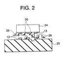
- Fig. 2 is a sectional view showing a state after the semiconductor chip 24 in the conventional flip chip type semiconductor device is removed from the mounting board 25.
- Fig. 2 when a chip is removed from a semiconductor device having an underfill resin, problems arise that the outer solder electrodes 13 remain buried in the underfill resin 26, the underfill resin 26 and the mounting board 25 are damaged and so forth. Therefore, the non-defective semiconductor chip 24 cannot be reused. With the above-described reasons, it is difficult to reuse a non-defective flip chip type semiconductor chip in the conventional technique.
- the passivation film is formed for the purpose of protecting the active region of the semiconductor chip 24 and composed of PI (polyimide) organic material or inorganic material such as an SiO material such as SiO, SiO 2 or the like. Furthermore, thermal and mechanical loads applied to the outer solder electrodes 13 are transmitted to the semiconductor chip 24, and thus a non-defective semiconductor chip 24 may become defective. In this case, peripheral devices including the mounting board 25 may also become defective.
- An object of the present invention is to provide a low-cost flip chip type semiconductor device in which an underfill resin is not used, mounting reliability is excellent since cracks due to a thermal stress can be prevented at the interface between a semiconductor chip and solder bumps and the semiconductor chip can be recovered, and a method of manufacturing the same.
- the flip chip type semiconductor device comprises a semiconductor chip provided with pad electrodes, an insulating resin layer covering a semiconductor chip surface on a side on which the pad electrodes are provided, metallic posts which penetrates through this insulating resin layer and are connected to the pad electrodes and electrodes which are provided on the insulating resin layer surface and connected to the metallic posts.
- the metallic post has a first portion buried in the insulating resin layer and a second portion projected from the insulating resin layer. It is noted that when “metal” is referred to in the present invention, not only pure metals but also alloys are included.
- a mounted semiconductor chip can be recovered since an underfill resin is not provided. Furthermore, since an underfill resin is not provided, there is no problem of a peeling phenomenon due to voids in the underfill resin or defective bonding between the underfill resin and a semiconductor chip or a mounting board. Furthermore, an insulating resin layer and metallic posts are disposed between the pad electrodes of the semiconductor chip and externally exposed electrodes. Ends of the metallic posts are projected from the insulating resin layer surface. Therefore, a layer composed of the metallic posts and the insulating resin layer serves as a stress relaxation layer so that thermal and mechanical loads imposed on the externally exposed electrodes can be prevented from transmitting to a semiconductor chip.
- centroids of the aforementioned first and second portions may be deviated from each other in a plane view. Consequently, the metallic post can be divided into two portions. Therefore, thermal and mechanical loads transmitted to the semiconductor chip via the metallic post can be further reduced and the aforementioned effect can be further enhanced.
- a plurality of recessed portions are formed in the surface of a metallic substrate, and a metallic post is formed on the surface of each recessed portion. Then, this metallic post and a pad electrode of a semiconductor chip are connected, an insulating resin layer is formed by filling an insulating resin into a space between the metallic substrate and the semiconductor chip, the metallic substrate is removed and electrodes are formed on the metallic post.
- a plurality of projected portions on a first surface of a metallic substrate, a plurality of projected portions corresponding to the projected portions formed on the first surface are formed on a second surface of the metallic substrate, and the projected portions formed on the first surface and pad electrodes of a semiconductor chip are connected with each other.
- an insulating resin layer is formed by filling an insulating resin into a space between the metallic substrate and the semiconductor chip, the projected portions are partitioned by removing portions of the metallic substrate other than the projected portions and electrodes are formed on the projected portions formed on the second surface of the metallic substrate.
- the aforementioned flip chip type semiconductor device can be efficiently fabricated.
- the plurality of projected portions may be formed by forming a resist for masking regions where the projected portions are to be formed and etching the metallic substrate by using this resist as a mask.
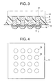
- Fig. 3 is a sectional view showing a flip chip type semiconductor device according to the first embodiment.
- a semiconductor chip 10 is provided with a plurality of pad electrodes 31 on one surface thereof and a solder electrode 9 is connected to each pad electrode 31.
- a metallic post 8 is further connected to each solder electrode 9.
- An insulating resin layer 11 is coated on a surface of the semiconductor chip 10 on a side on which the pad electrodes 31 are formed. And, whole the pad electrode 31 and solder electrode 9 and part of the metallic post 8 are buried in the insulating resin layer 11. The remaining portion of the metallic post 8 is projected from the insulating resin layer 11 to form a protrusion 12.
- a second plating film 7 and first plating film 6 are coated on the protrusion 12 of the metallic post 8.
- An outer solder electrode 13 is connected to the first plating film 6. The outer solder electrode 13 is formed so as to cover the protrusion 12.
- Fig. 4 is a plan view showing the flip chip type semiconductor device of the embodiment viewed from the outer solder electrode 13 side. As shown in Fig. 4, in this flip chip type semiconductor device, the outer solder electrodes 13 are arranged in a matrix on the insulating resin layer 11.
- the height of the solder electrode 9 can be made about 100 ⁇ m
- the height of the metallic post 8 can be made about 100 ⁇ m
- the height of the portion of the metallic post 8 buried in the insulating resin layer 11 can be made about 80 ⁇ m
- the height of the portion projected from the surface of the insulating resin layer 11 can be made about 20 ⁇ m.
- the height of the outer solder electrode 13 can be made about 100 ⁇ m and the diameter of the metallic post 8 can be made, for example, 150 ⁇ m.
- the thickness of the semiconductor chip 10 can be made, for example, about 50 to 725 ⁇ m.
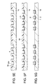
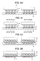
- Figs. 5A to 5K are sectional views showing the method of manufacturing the flip chip type semiconductor device according to the embodiment in the order of manufacturing process steps.
- a resist 2a is formed on a surface of a metallic substrate 1a.
- the material of the metallic substrate 1a is not particularly limited, but copper, nickel, gold, tin, lead, 42 alloy containing these or the like, which can be easily etched later, is preferable.
- the thickness of the metallic substrate 1a is not particularly limited either, but a thickness which affects etching as little as possible and can be easily handled is preferable. Subsequently, as shown in Fig.
- this resist 2a is exposed and developed to form a patterned resist 4a having prescribed apertures. Then, as shown in Fig. 5D, half-etching is selectively performed by using this resist 4a as a mask to form recessed portions 30a at positions at which plating and bumps are to be formed later.
- This recessed portion 30a needs a size enough to have a structure of an outer post later.
- a first plating film 6 is formed in the recessed portion 30a.
- the resist 4a used in the aforementioned half-etching is utilized as a mask as it is.
- a material of the first plating film 6 a metal with which only the metallic substrate 1a can be selectively etched so that the first plating film 6 remains even when the metallic substrate 1a is etched in a later process, for example, Au is used.
- a second plating film 7 may be formed on the first plating film 6. This second plating film 7 is formed, for example, to improve plating stability when a metallic post 8 is formed in the next process.
- metallic posts 8 are formed by plating using the resist 4a as a mask.
- the material of the metallic post 8 is not particularly limited, but a material which has a favorable bonding characteristic with a chip to be mounted onto the metallic post 8 in a later process and has favorable conductivity, for example, Cu can be used. Or, solder plating may be formed on the metallic post 8.
- solder electrodes 9 are provided on pad electrodes 31 of a semiconductor chip 10 and the semiconductor chip 10 is mounted onto the metallic posts 8 by a chip bonder (not shown) and a reflow device (not shown) or the like. Then, the metallic posts 8 and the solder electrodes 9 are bonded by metallic bond by thermal treatment. However, if solder plating is formed on the metallic post 8, the pad electrode of the semiconductor chip 10 does not need to be provided with the solder electrode 9. Then, as shown in Fig. 5J, an insulating resin is filled between the semiconductor chip 10 and metallic substrate 1a to form an insulating resin layer 11 and cover the metallic post 8.
- Methods of filling the insulating resin include a method utilizing a capillary phenomenon, a transfer-sealing method and so forth.
- the insulating resin epoxy resins, silicon resins, polyimide resins, polyolefin resins, cyanate ester resins, phenol resins, naphthalene resins, fluorene resins or the like can be used. Subsequently, as shown in Fig. 5K, only the metallic substrate 1a is removed by etching.
- a solder ball is mounted on the protrusion 12 of the metallic post 8 and bonded to the metallic post 8 by a method such as a reflow treatment or the like to form an outer solder electrode 13.
- the metallic post 8 since the metallic post 8 has the protrusion 12 projected from the surface of the insulating resin layer 11, peeling of the outer solder electrode 13 from the metallic post 8 can be reliably prevented when a shearing stress is applied to the outer solder electrode 13 in the horizontal direction, as compared with a case where a protrusion 12 is not provided. That is, when a shearing stress exceeding a certain level is applied to the outer solder electrode 13, cracks occur at the interface between the first plating film 6 and the outer solder electrode 13. If the metallic post 8 does not have a protrusion 12, the cracks are propagated instantaneously and the outer solder electrode 13 peels from the metallic post 8.
- the metallic post 8 since the metallic post 8 has the protrusion 12 in the embodiment, this propagation of cracks can be prevented. Furthermore, since a contact area between the first plating film 6 and the outer solder electrode 13 is increased due to the presence of the protrusion 12, the solder bond strength is increased. Therefore, the bond strength between the metallic post 8 and the outer solder electrode 13 is improved, and thus mounting reliability of a flip chip type semiconductor device is improved.
- the height of the portion of the metallic post 8 exposed from the surface of the insulating resin layer 11, that is, the height of the protrusion 12 is preferably 7 to 50% of the height of the outer solder electrode 13, that is, the distance from the end of the outer solder electrode 13 to the surface of the insulating resin layer 11.
- the ratio lower than 7% results in insufficient effects of withstanding a shearing stress applied to the interface between the metallic post 8 and the outer solder electrode 13 and preventing propagation of cracks occurring at the interface.
- the contact area between the mounting board and the solder is reduced if the ratio exceeds 50%, the bond strength is unfavorably degraded. It is more preferable that the ratio is 20 to 50%.
- the external terminal is made higher due to the metallic post 8 and the insulating resin layer 11 in the flip chip type semiconductor device of the embodiment. Therefore, when the flip chip type semiconductor device of the the embodiment is mounted onto the multi-layer wiring board on the end user side, the stand-off height between the multi-layer wiring board and the semiconductor chip is increased. Consequently, a buffer effect is provided against a stress which occurs due to a difference between thermal expansion coefficients of the multi-layer wiring board and the flip chip semiconductor device, and thus mounting reliability of the flip chip type semiconductor device can be improved. Also, the passivation film and the active region surface under the passivation film of the semiconductor chip 10 can be protected from thermal and mechanical loads generated when the semiconductor chip 10 is recovered. In order to obtain the aforementioned effects, the height of the metallic post 8 is preferably 100 ⁇ m or higher.
- the metallic post 8 and the insulating resin layer 11 serve as a stress relaxation layer in the flip chip type semiconductor device of the embodiment, the underfill resin filled between semiconductor chip and multi-layer wiring board in the conventional device is not required. Therefore, if the semiconductor chip 10 is mounted and then a defect is detected in a portion other than the semiconductor chip 10, the semiconductor chip 10 can be peeled off from the mounting board, recovered and reused.
- the underfill resin is not provided in the flip chip type semiconductor device of the embodiment, there is no problem of a peeling phenomenon due to voids in the underfill resin or defective bonding between the underfill resin and semiconductor chip or mounting board.
- metal plating can be easily provided to the exposed portion of the metallic post.
- Advantages of providing the metal plating include that an insulating oxide film can be prevented from being formed on the metallic post by providing plating using non-oxidative metal such as Au or the like and that the metallic post can be protected from a thermal stress applied to the exposed portion of the metallic post by providing plating using high-hardness metal such as Ni or the like. Consequently, mounting reliability of the semiconductor device can be further improved.
- Fig. 6 is a sectional view showing a flip chip type semiconductor device according to the embodiment.
- a semiconductor chip 10 provided with a plurality of pad electrodes 31 on one surface thereof is provided and a solder electrode 9 is connected to each pad electrode 31.
- a metallic post 16b is connected to each solder electrode 9.
- the surface of the semiconductor chip 10 on a side on which pad electrodes 31 are formed is coated with an insulating resin layer 11 and whole the pad electrode 31 and solder electrode 9 and part of the metallic post 16b are buried in the insulating resin layer 11.
- the remaining portion of the metallic post 16b is projected from the insulating resin layer 11 to form a protrusion.
- An outer solder electrode 13 is formed so as to cover the protrusion.
- the plan view of this flip chip type semiconductor device viewed from the outer solder electrode 13 side is the same as shown in Fig. 4.
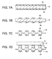
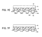
- Figs. 7A to 7F are sectional views showing a method of manufacturing the semiconductor device according to the second embodiment in the order of manufacturing process steps.
- a metallic substrate 1b is fabricated as in the case of the first embodiment.
- a metal of this metallic substrate 1b for example, Cu is used.
- the thickness of the metallic substrate 1b is preferably 100 ⁇ m or more.
- the front surface and the rear surface of the metallic substrate 1b are coated with resists 2b and 3b, respectively.
- the resists 2b and 3b are exposed and developed to form patterned resists 4b and 5b.
- the metallic substrate 1b is etched from both surfaces. Consequently, a temporary substrate 14b is formed.
- the etching amount at this time is not particularly limited, but the etching amount of the front side (resist 4b side) determines the height of the metallic post portion covered by an insulating resin layer to be formed later.
- the etching amount of the rear side (resist 5b side) determines the height of the metallic post portion projected from the insulating resin layer surface. Therefore, the etching amounts are determined in consideration to these heights.
- the semiconductor chip 10 is mounted onto the temporary substrate 14b so that the solder electrode 9 provided on the pad electrode 31 of the semiconductor chip 10 and the projected portion 15b of the temporary substrate 14b are brought into contact, and the solder electrode 9 and the projected portion 15b are bonded by metallic bond by means such as reflow and thermal pressing or the like.
- an insulating resin is filled between the temporary substrate 14b and the semiconductor chip 10 to form an insulating resin layer 11.
- the rear surface of the temporary substrate 14b is etched by using the resist 5b as a mask to remove a metal between the projected portions 15b of the temporary substrate 14b and form metallic posts 16b.
- the resists on both sides are removed in the process shown in Fig. 7D.
- metal portions between the metallic posts 16b are removed by etching whole the rear surface.
- an outer solder electrode 13 is formed on the protrusion of the metallic post 16b by a reflow treatment of a solder paste or solder balls or the like to obtain the flip chip type semiconductor device of the second embodiment.
- the end of the metallic post 16b can be projected highly from the surface of the insulating resin layer 11. Consequently, a structure can be obtained which is resistant to cracks, breaking or the like of solder balls occurring due to thermal and mechanical loads upon mounting of the device on the multi-layer wiring board.
- the metallic post is formed by plating in the first embodiment
- the metallic post is formed from the metallic substrate in the embodiment. Therefore, variations in heights of the metallic posts can be easily prevented and higher metallic posts can be formed by a method such as an etching method, which is relatively easy and inexpensive.
- Fig. 8 is a sectional view showing a flip chip type semiconductor device according to the embodiment.
- a semiconductor chip 10 provided with a plurality of pad electrodes 31 on one surface thereof is provided and a solder electrode 9 is connected to each pad electrode 31.
- a metallic post 16c is connected to each solder electrode 9 via a metal plating film 17.
- the surface of the semiconductor chip 10 on a side on which the pad electrodes 31 are formed is coated with an insulating resin layer 11 and whole the pad electrode 31 and solder electrode 9 and part of the metallic post 16c are buried in the insulating resin layer 11.
- the remaining portion of the metallic post 16c is projected from the insulating resin layer 11 and forms a protrusion.
- This protrusion is coated with a metal plating film 17 and an outer solder electrode 13 is formed so as to cover the metal plating film 17.
- the plan view of this flip chip type semiconductor device viewed from the outer solder electrode 13 side is the same as shown in Fig. 4.
- Figs. 9A and 9B are sectional views showing a method of manufacturing the flip chip type semiconductor device according to the third embodiment in the order of manufacturing process steps.
- the front surface and the rear surface of a metallic substrate 1c are coated with resists and the resists are exposed and developed to form resists 4c and 5c whose patterns are inverted to those of the resists 4b and 5b in the second embodiment.
- a metal plating film 17 is formed on portions on which the resists 4c and 5c are not formed by using the resists 4c and 5c as masks.
- a metal constituting this metal plating film 17 a metal which is resistant to an etchant of the metallic substrate 1c is selected.
- a temporary substrate 14c which is the same as the temporary substrate 14b of the second embodiment shown in Fig. 7C and has a metal plating layer 17 disposed on the surface of the projected portion can be formed.
- a flip chip type semiconductor device can be obtained by the same processes as those shown in Figs. 7D to 7F and Fig. 6 in the second embodiment. That is, the semiconductor chip 10 is mounted onto the temporary substrate 14c so that the solder electrode 9 provided on the pad electrode 31 of the semiconductor chip 10 and the projected portion 15c of the temporary substrate 14c are brought into contact. Then, the solder electrode 9 and the projected portion 15c are bonded by metallic bond by means such as reflow and thermal pressing or the like. Subsequently, an insulating resin is filled between the temporary substrate 14c and semiconductor chip 10 to form an insulating resin layer 11.
- the rear surface of the temporary substrate 14c is etched by using the metal plating film 17 as a mask to remove a metal between the projected portions 15c of the temporary substrate 14c and form metallic posts 16c.
- an outer solder electrode 13 is formed on the portion of the metallic post 16c projected from the insulating resin layer 11 by a reflow treatment of a solder paste or solder balls or the like to obtain the flip chip type semiconductor device of the third embodiment as shown in Fig. 8.
- the resist can be removed in an earlier manufacturing process as compared with the second embodiment. Therefore, the temporary substrate can be maintained for a long period and the temporary substrate can be easily handled. Furthermore, the metal plating layer 17 can be easily formed on the surface of the metallic post 16c.
- Fig. 10 is a sectional view showing a flip chip type semiconductor device according to the embodiment.
- the flip chip type semiconductor device according to the embodiment has a structure in which a portion 18d buried in an insulating resin layer 11 of a metallic post 16d and a portion 19d projected from a surface of the insulating resin layer 11 are deviated from each other.
- Fig. 11 is a plan view of this flip chip type semiconductor device viewed from the outer solder electrode 13 side.
- the portions 18d of the metallic posts 16d (see Fig. 10) are buried in a matrix in the surface of the insulating resin layer 11.
- outer solder electrodes 13 are disposed in a matrix corresponding to the portions 18d. Respective portions 18d and respective outer solder electrodes 13 are deviated from each other.
- the construction of the flip chip type semiconductor device according to the embodiment other than the above is the same as the construction of the flip chip type semiconductor device according to the second embodiment.
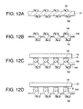
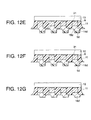
- Figs. 12A to 12G are sectional views showing a method of manufacturing the flip chip type semiconductor device according to the fourth embodiment in the order of manufacturing process steps.
- Fig. 12A both the front surface and the rear surface of a metallic substrate 1d are coated with resists and the resists are exposed and developed to form patterned resists 4d and 5d.
- apertures of the resists in the front surface and the rear surface are deviated.
- Positions of the apertures of the resist 5d need to correspond to positions of the apertures of the resist 4d, but the direction and distance of deviation can be arbitrarily set.
- the front surface and the rear surface of the metallic substrate 1d are selectively etched by using the resists 4d and 5d, respectively, as masks to obtain such a temporary substrate 14d as shown in Fig. 12B.
- the subsequent processes are the same as those in the second and third embodiments. That is, as shown in Fig. 12C, the resist 4d formed on the front surface of the temporary substrate 14d is removed to expose the surface portion of the temporary substrate 14d. Subsequently, a semiconductor chip 10 is mounted onto the temporary substrate 14d so that the solder electrode 9 formed on the pad electrode 31 of the semiconductor chip 10 and the projected portion 15d of the temporary substrate 14d are brought into contact with each other. Subsequently, as shown in Fig. 12D, the solder electrode 9 is bonded by metallic bond to the temporary substrate 14d by means such as reflow and thermal pressing or the like. Then, as shown in Fig.
- an insulating resin is filled between the temporary substrate 14d and semiconductor chip 10 to form an insulating resin layer 11.
- the rear surface of the temporary substrate 14d is etched by using the resist 5d as a mask to remove the metal between the projected portions 15d of the temporary substrate 14d and form metallic posts 16d.
- the resist 5d is removed.
- an outer solder electrode 13 is formed on the exposed portion of the metallic post 16d by a reflow treatment of a solder paste or solder balls to obtain the flip chip type semiconductor device of the embodiment.
- the metallic post 16d is composed of two portions 18d and 19d, which are deviated from each other. Therefore, a stress relaxation property at the time of reflow or the like can be improved. Thus, thermal and mechanical stresses applied to the exposed portion of the metallic post 16d can be prevented from transmitting to the semiconductor chip 10.
- the processes shown in Figs. 12A and 12B until the temporary substrate 14d is formed can be substituted for the processes shown in Figs. 9A and 9B, in which the metal plating film is formed and then etched to form the temporary substrate in the third embodiment.
- Fig. 13 is a sectional view showing a flip chip type semiconductor device according to the embodiment.
- a semiconductor chip 10 provided with a plurality of pad electrodes 31 on one surface thereof is provided and a solder electrode 9 is connected to each pad electrode 31.
- One end of a metallic post 16b is connected to each solder electrode 9 while a metallic post 16e is connected to the other end of the metallic post 16b by a solder 32.
- the surface of the semiconductor chip 10 on a side on which the pad electrodes 31 are formed is coated with an insulating resin layer 11 and whole of the pad electrode 31, solder electrode 9 and metallic post 16b and part of the metallic post 16e are buried in the insulating resin layer 11.
- the remaining portion of the metallic post 16e is projected from the insulating resin layer 11 and forms a protrusion.
- an outer solder electrode 13 is formed so as to cover this protrusion. That is, the pad electrode 31, solder electrode 9, metallic post 16b, metallic post 16e and outer solder electrode 13 are connected in series in this order. Since the metallic post 16e is formed so as to stack on the metallic post 16b in the flip chip type semiconductor device 20e, the distance between the solder electrode 9 and outer solder electrode 13 is increased.
- a plan view of this flip chip type semiconductor device viewed from the outer solder electrode 13 side is the same as the one shown in Fig. 4.
- Figs. 14A to 14C are sectional views showing a method of manufacturing the semiconductor device according to the fifth embodiment in the order of manufacturing process steps.
- a flip chip type semiconductor device shown in the second embodiment is fabricated. That is, as shown in Fig. 7A, the front surface and the rear surface of a metallic substrate 1b are coated with resists 2b and 3b, respectively, and, as shown in Fig. 7B, the resists 2b and 3b are exposed and developed to form patterned resists 4b and 5b. Subsequently, as shown in Fig. 7C, the metallic substrate 1b is etched from both surfaces to form a temporary substrate 14b. Then, as shown in Fig.
- the resist 4b on the front surface is removed to expose the surface portion of the temporary substrate 14b.
- the semiconductor chip 10 is mounted so that the solder electrode 9 on the chip side and the projected portion 15b of the temporary substrate 14b are brought into contact and bonded by metallic bond by means such as reflow and thermal pressing or the like.
- an insulating resin is filled between the temporary substrate 14b and semiconductor chip 10 to form an insulating resin layer 11.
- the rear surface of the temporary substrate 14b is etched by using the resist 5b as a mask to form a metallic post 16b.
- an outer solder electrode 13 is formed on the exposed portion of the metallic post 16b by reflow treatment or the like of a solder paste or solder balls to obtain a flip chip type semiconductor device 20b.
- the temporary substrate 14b is bonded to the flip chip type semiconductor device 20b by utilizing the solder 32 constituting the outer solder electrode 13.
- an insulating resin is filled between the flip chip type semiconductor device 20b and the temporary substrate 14b to form an insulating resin layer 11.
- etching is performed from the temporary substrate 14b side to form a metallic post 16e. Further, the resist 5b on the temporary substrate 14b is removed.
- an outer solder electrode 13 is formed on the protrusion of the metallic post 16e by a reflow treatment or the like of a solder paste or solder balls to obtain the flip chip type semiconductor device 20e of the fifth embodiment.
- the height of the metallic post can be further increased by repeating the manufacturing processes in accordance with the fifth embodiment.
- the flip chip type semiconductor device 20b is first fabricated by the method shown in the second embodiment, but the flip chip type semiconductor device fabricated by the method shown in the first, third or fourth embodiment or the sixth or seventh embodiment described later can also be used.
- the processes of forming the temporary substrate 14b can also be substituted for the processes in the third embodiment shown in Figs. 9A and 9B, in which the metal plating film is formed and then etched to form a temporary substrate.
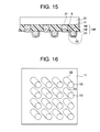
- Fig. 15 is a sectional view showing a flip chip type semiconductor device according to the embodiment.
- a metallic post 16f is constituted by a portion 18f buried in an insulating resin layer 11, a portion 19f projected from the surface of the insulating resin 11 and metal wiring 23 disposed on the surface of the insulating resin 11.
- the side face of the portion 18f is located outside the side face of the portion 19f in a plane view while the portion 18f is connected to the portion 19f by metal wiring 23.
- an outer solder electrode 13 is formed so as to cover the portion 19f.
- Fig. 16 is a plan view of this flip chip type semiconductor device viewed from the outer solder electrode 13 side. As shown in Fig. 16, a plurality of outer solder electrodes 13 are arranged in a matrix on the insulating resin layer 11 in the flip chip type semiconductor device of the embodiment. Metal wiring 23 is connected to each outer solder electrode 13.
- the construction of the flip chip type semiconductor device according to the embodiment other than the above is the same as that of the flip chip type semiconductor device of the above-described second embodiment.
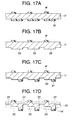
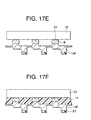
- FIGs. 17A to 17F are sectional views showing a method of manufacturing the semiconductor device according to the sixth embodiment in the order of manufacturing process steps.
- the front surface and the rear surface of a metallic substrate if are coated with resists and the resists are exposed and developed to form patterned resists 4f and 5f as shown in Fig. 17A.
- the rear surface is etched by using the resist 5f as a mask. Consequently, the metallic substrate if is formed in a shape that an island-like projected portion 33 is formed on the rear surface. Subsequently, the resist 5f is removed.
- the same construction can be obtained by forming a resist inverted to the resist pattern of the resist 5f, performing plating on the rear surface, removing the resist of the rear surface and then performing etching by using the plating film as a mask.
- a resist 21 is formed at a position deviated from the resist 4f on the island-like projected portion 33 formed on the rear surface.
- regions 22 on the front surface and the rear surface are etched by using the resists 4f and 21 as masks to obtain a temporary substrate 14f.
- a semiconductor chip 10 is mounted on the temporary substrate 14f and the semiconductor chip 10 is bonded to the temporary substrate 14f.
- an insulating resin layer 11 is provided between the semiconductor chip 10 and temporary substrate 14f.
- the rear surface of the temporary substrate 14f is selectively etched by using the resist 21 as a mask to partition the metallic post 16f. Further, the resist 21 is removed. Then, an outer solder electrode 13 is formed so as to cover the portion 19f of the metallic post 16f projected from the insulating resin layer 11 to obtain the flip chip type semiconductor device 20f of the sixth embodiment.
- the externally exposed portion 19f of the metallic post 16f and the portion 18f buried in the insulating resin are connected via metal wiring 23. Consequently, an effect of relaxing a thermal stress generated at the time of reflow or the like can be further improved. An effect of preventing thermal and mechanical stresses applied to the externally exposed portion from being directly transmitted to the semiconductor chip 10 can also be further improved.
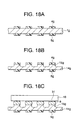
- FIGs. 18A to 18F are sectional views showing a method of manufacturing a flip chip type semiconductor device according to the seventh embodiment in the order of manufacturing process steps. According to the method of the embodiment, various forms of flip chip type semiconductor devices can be fabricated. The method of manufacturing a flip chip type semiconductor device of the seventh embodiment will be described as an example thereof with reference to a case where the flip chip type semiconductor device 20b shown in the second embodiment is fabricated. First, as shown in Fig. 18A, resists 4g and 5g are formed on both sides of a metallic substrate 1g as in the case of the second embodiment.
- a temporary substrate 14g having a projected portion 15g formed on a surface thereof is fabricated as shown in Fig. 18B.
- the semiconductor chip 10 is placed on the surface of the temporary substrate 14g so that a solder electrode 9 formed on a pad electrode 31 of a semiconductor chip 10 is brought into contact with the projected portion 15g.
- the solder electrode 9 is heated so that the semiconductor chip 10 is bonded to the temporary substrate 14g.
- an insulating resin layer 11 is formed between the semiconductor chip 10 and temporary substrate 14g.
- etching is performed from the rear surface by using the resist 5g as a mask. Consequently, metal is removed from the portion other than the projected portion 15g of the metallic substrate 1g to form a metallic post 16g.
- the resist 5g is removed and the outer solder electrode 13 is formed to obtain the flip chip type semiconductor device 20b.
- the construction of the flip chip type semiconductor device obtained by the embodiment is the same as the one obtained by the second embodiment.
- the rear surface of the temporary substrate 14g is etched. Consequently, the strength of the temporary substrate 14g can be maintained until the insulating resin layer 11 is formed. As a result, handling of the temporary substrate 14g can be improved. Furthermore, the etching amount when the temporary substrate 14g is formed does not need to be precisely controlled. As a result, the flip chip type semiconductor device can be easily fabricated and the fabrication time can be shortened.
- fabrication of the flip chip type semiconductor device shown in the second embodiment is exemplified, but the method shown in the embodiment is applicable to a case where the flip chip type semiconductor devices shown in the third to sixth embodiments are fabricated.
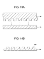
- FIGs. 19A and 19B are sectional views showing a method of manufacturing a semiconductor device according to the eighth embodiment in the order of manufacturing process steps.
- the method of manufacturing a flip chip type semiconductor device according to the eighth embodiment will be described by exemplifying the case where the same flip chip type semiconductor device as shown in the second embodiment is fabricated.
- Fig. 19A the surface of a metallic substrate 1h is pressed by a mold 28 having a recessed portion. Consequently, as shown in Fig. 19B, a temporary substrate 14h having a projected portion 15h is fabricated.
- the semiconductor chip is placed on the surface temporary substrate 14h, heated and bonded and an insulating resin is filled between the semiconductor chip and the temporary substrate 14h to form an insulating resin layer. Subsequently, etching is performed on the whole rear surface and metal is removed from the portion other than the projected' portion 15h of the metallic substrate 1h to form a metallic post. Then, an outer solder electrode is formed to obtain the flip chip type semiconductor device.
- the construction of the flip chip type semiconductor device obtained by the embodiment is the same as the one obtained by the second embodiment shown in Fig. 6.
Landscapes
- Wire Bonding (AREA)
- Encapsulation Of And Coatings For Semiconductor Or Solid State Devices (AREA)
- Structures Or Materials For Encapsulating Or Coating Semiconductor Devices Or Solid State Devices (AREA)
Applications Claiming Priority (2)
| Application Number | Priority Date | Filing Date | Title |
|---|---|---|---|
| JP2000157432A JP2001338947A (ja) | 2000-05-26 | 2000-05-26 | フリップチップ型半導体装置及びその製造方法 |
| JP2000157432 | 2000-05-26 |
Publications (2)
| Publication Number | Publication Date |
|---|---|
| EP1160856A2 true EP1160856A2 (fr) | 2001-12-05 |
| EP1160856A3 EP1160856A3 (fr) | 2003-02-12 |
Family
ID=18662064
Family Applications (1)
| Application Number | Title | Priority Date | Filing Date |
|---|---|---|---|
| EP01113016A Withdrawn EP1160856A3 (fr) | 2000-05-26 | 2001-05-28 | Dispositif semi-conducteur Flip chip et son procédé de fabrication |
Country Status (7)
| Country | Link |
|---|---|
| US (3) | US6503779B2 (fr) |
| EP (1) | EP1160856A3 (fr) |
| JP (1) | JP2001338947A (fr) |
| KR (1) | KR100432643B1 (fr) |
| CN (1) | CN1326225A (fr) |
| SG (1) | SG87930A1 (fr) |
| TW (1) | TW494557B (fr) |
Families Citing this family (94)
| Publication number | Priority date | Publication date | Assignee | Title |
|---|---|---|---|---|
| US6818545B2 (en) | 2001-03-05 | 2004-11-16 | Megic Corporation | Low fabrication cost, fine pitch and high reliability solder bump |
| KR100445072B1 (ko) * | 2001-07-19 | 2004-08-21 | 삼성전자주식회사 | 리드 프레임을 이용한 범프 칩 캐리어 패키지 및 그의제조 방법 |
| US20070108609A1 (en) * | 2001-07-19 | 2007-05-17 | Samsung Electronics Co., Ltd. | Bumped chip carrier package using lead frame and method for manufacturing the same |
| JP2003151981A (ja) * | 2001-11-16 | 2003-05-23 | Shinko Electric Ind Co Ltd | 半導体装置およびその製造方法 |
| JP2003179099A (ja) * | 2001-12-12 | 2003-06-27 | Toshiba Corp | 半導体装置およびその製造方法 |
| TWI245402B (en) * | 2002-01-07 | 2005-12-11 | Megic Corp | Rod soldering structure and manufacturing process thereof |
| JP3829325B2 (ja) | 2002-02-07 | 2006-10-04 | 日本電気株式会社 | 半導体素子およびその製造方法並びに半導体装置の製造方法 |
| KR100439407B1 (ko) * | 2002-04-11 | 2004-07-09 | 삼성전기주식회사 | 반도체소자 패키지 제조방법 |
| US6943056B2 (en) * | 2002-04-16 | 2005-09-13 | Renesas Technology Corp. | Semiconductor device manufacturing method and electronic equipment using same |
| US7071537B2 (en) * | 2002-05-17 | 2006-07-04 | Ixys Corporation | Power device having electrodes on a top surface thereof |
| US20040232562A1 (en) * | 2003-05-23 | 2004-11-25 | Texas Instruments Incorporated | System and method for increasing bump pad height |
| TWI250640B (en) | 2003-06-19 | 2006-03-01 | Samsung Electronics Co Ltd | Bipolar junction transistors and methods of manufacturing the same |
| TWI367566B (en) * | 2004-05-06 | 2012-07-01 | United Test And Assembly Ct | Structurally-enhanced integrated circuit package and method of manufacture |
| JP2006093575A (ja) * | 2004-09-27 | 2006-04-06 | Hitachi Cable Ltd | 半導体装置およびその製造方法 |
| CN100461354C (zh) * | 2004-09-28 | 2009-02-11 | 相丰科技股份有限公司 | 适用集成电路及发光二极管的封装方法 |
| US7246434B1 (en) | 2004-10-11 | 2007-07-24 | Pericom Semiconductor Corp. | Method of making a surface mountable PCB module |
| US7523852B2 (en) * | 2004-12-05 | 2009-04-28 | International Business Machines Corporation | Solder interconnect structure and method using injection molded solder |
| US8033016B2 (en) * | 2005-04-15 | 2011-10-11 | Panasonic Corporation | Method for manufacturing an electrode and electrode component mounted body |
| US7851348B2 (en) | 2005-06-14 | 2010-12-14 | Abhay Misra | Routingless chip architecture |
| US7838997B2 (en) | 2005-06-14 | 2010-11-23 | John Trezza | Remote chip attachment |
| US7767493B2 (en) | 2005-06-14 | 2010-08-03 | John Trezza | Post & penetration interconnection |
| US7534722B2 (en) | 2005-06-14 | 2009-05-19 | John Trezza | Back-to-front via process |
| US7786592B2 (en) | 2005-06-14 | 2010-08-31 | John Trezza | Chip capacitive coupling |
| US7687400B2 (en) | 2005-06-14 | 2010-03-30 | John Trezza | Side stacking apparatus and method |
| US7781886B2 (en) | 2005-06-14 | 2010-08-24 | John Trezza | Electronic chip contact structure |
| US7946331B2 (en) | 2005-06-14 | 2011-05-24 | Cufer Asset Ltd. L.L.C. | Pin-type chip tooling |
| JP5253158B2 (ja) * | 2005-06-14 | 2013-07-31 | キューファー アセット リミテッド. エル.エル.シー. | ポストおよびペネトレーション相互接続 |
| US8456015B2 (en) * | 2005-06-14 | 2013-06-04 | Cufer Asset Ltd. L.L.C. | Triaxial through-chip connection |
| US7521806B2 (en) | 2005-06-14 | 2009-04-21 | John Trezza | Chip spanning connection |
| US7560813B2 (en) | 2005-06-14 | 2009-07-14 | John Trezza | Chip-based thermo-stack |
| JP2007048887A (ja) * | 2005-08-09 | 2007-02-22 | Seiko Epson Corp | 半導体装置およびその製造方法 |
| KR20080049807A (ko) * | 2005-10-03 | 2008-06-04 | 로무 가부시키가이샤 | 반도체 장치 |
| US7687397B2 (en) | 2006-06-06 | 2010-03-30 | John Trezza | Front-end processed wafer having through-chip connections |
| KR101175393B1 (ko) * | 2006-10-17 | 2012-08-20 | 쿠퍼 에셋 엘티디. 엘.엘.씨. | 웨이퍼 비아 형성 |
| US20080135990A1 (en) * | 2006-12-07 | 2008-06-12 | Texas Instruments Incorporated | Stress-improved flip-chip semiconductor device having half-etched leadframe |
| DE102007034402B4 (de) * | 2006-12-14 | 2014-06-18 | Advanpack Solutions Pte. Ltd. | Halbleiterpackung und Herstellungsverfahren dafür |
| US7705613B2 (en) * | 2007-01-03 | 2010-04-27 | Abhay Misra | Sensitivity capacitive sensor |
| CN100539101C (zh) * | 2007-01-18 | 2009-09-09 | 南茂科技股份有限公司 | 一致化凸块接合高度的高频集成电路封装构造及制造方法 |
| US7705632B2 (en) * | 2007-02-15 | 2010-04-27 | Wyman Theodore J Ted | Variable off-chip drive |
| US7803693B2 (en) * | 2007-02-15 | 2010-09-28 | John Trezza | Bowed wafer hybridization compensation |
| US7598163B2 (en) * | 2007-02-15 | 2009-10-06 | John Callahan | Post-seed deposition process |
| US7670874B2 (en) * | 2007-02-16 | 2010-03-02 | John Trezza | Plated pillar package formation |
| EP1968109A3 (fr) * | 2007-03-08 | 2012-08-01 | Nissan Motor Co., Ltd. | Dispositif semi-conducteur et son procédé de fabrication |
| US7850060B2 (en) * | 2007-04-05 | 2010-12-14 | John Trezza | Heat cycle-able connection |
| US7748116B2 (en) * | 2007-04-05 | 2010-07-06 | John Trezza | Mobile binding in an electronic connection |
| US7960210B2 (en) * | 2007-04-23 | 2011-06-14 | Cufer Asset Ltd. L.L.C. | Ultra-thin chip packaging |
| US20080261392A1 (en) * | 2007-04-23 | 2008-10-23 | John Trezza | Conductive via formation |
| US8390107B2 (en) * | 2007-09-28 | 2013-03-05 | Intel Mobile Communications GmbH | Semiconductor device and methods of manufacturing semiconductor devices |
| US7993979B2 (en) * | 2007-12-26 | 2011-08-09 | Stats Chippac Ltd. | Leadless package system having external contacts |
| US8492883B2 (en) * | 2008-03-14 | 2013-07-23 | Advanced Semiconductor Engineering, Inc. | Semiconductor package having a cavity structure |
| US20100044850A1 (en) * | 2008-08-21 | 2010-02-25 | Advanced Semiconductor Engineering, Inc. | Advanced quad flat non-leaded package structure and manufacturing method thereof |
| US8124447B2 (en) | 2009-04-10 | 2012-02-28 | Advanced Semiconductor Engineering, Inc. | Manufacturing method of advanced quad flat non-leaded package |
| US20110163430A1 (en) * | 2010-01-06 | 2011-07-07 | Advanced Semiconductor Engineering, Inc. | Leadframe Structure, Advanced Quad Flat No Lead Package Structure Using the Same, and Manufacturing Methods Thereof |
| US8264089B2 (en) | 2010-03-17 | 2012-09-11 | Maxim Integrated Products, Inc. | Enhanced WLP for superior temp cycling, drop test and high current applications |
| US8476772B2 (en) * | 2010-09-09 | 2013-07-02 | Stats Chippac, Ltd. | Semiconductor device and method of forming base substrate with recesses for capturing bumped semiconductor die |
| US8304277B2 (en) | 2010-09-09 | 2012-11-06 | Stats Chippac, Ltd. | Semiconductor device and method of forming base substrate with cavities formed through etch-resistant conductive layer for bump locking |
| CN101976663B (zh) * | 2010-09-27 | 2012-07-25 | 清华大学 | 一种无基板的倒装芯片的芯片尺寸封装结构 |
| CN101976662B (zh) * | 2010-09-27 | 2012-07-25 | 清华大学 | 一种无基板的输出端扇出型倒装芯片封装结构 |
| US9165795B2 (en) * | 2010-12-09 | 2015-10-20 | Cypress Semiconductor Corporation | High performance low profile QFN/LGA |
| KR101048427B1 (ko) | 2010-12-23 | 2011-07-11 | 주식회사 고려반도체시스템 | 플립칩 본딩용 기판 이송 장치 및 이를 이용한 플립칩 본딩 방법 |
| JP2012169440A (ja) * | 2011-02-14 | 2012-09-06 | Fujitsu Semiconductor Ltd | 半導体装置及びその製造方法 |
| KR101161204B1 (ko) | 2011-04-21 | 2012-07-02 | 주식회사 고려반도체시스템 | 플립칩 본딩용 기판 이송 장치 |
| KR101182575B1 (ko) | 2011-04-21 | 2012-09-18 | 주식회사 고려반도체시스템 | 플립칩 본딩 방법 |
| KR101182576B1 (ko) | 2011-04-21 | 2012-09-18 | 주식회사 고려반도체시스템 | 플립칩 본딩 방법 |
| CN102891131B (zh) | 2011-07-22 | 2017-07-14 | 先进封装技术私人有限公司 | 用于制造半导体封装元件的半导体结构及其制造方法 |
| TWI508241B (zh) | 2011-10-20 | 2015-11-11 | 先進封裝技術私人有限公司 | 封裝基板、封裝基板製程、半導體元件之封裝結構及其製程 |
| TWI500124B (zh) | 2011-11-29 | 2015-09-11 | 先進封裝技術私人有限公司 | 基板結構、半導體封裝元件及基板結構之製造方法 |
| KR101255954B1 (ko) | 2011-12-22 | 2013-04-23 | 삼성전기주식회사 | 인쇄회로기판 및 인쇄회로기판 제조 방법 |
| US8952413B2 (en) | 2012-03-08 | 2015-02-10 | Micron Technology, Inc. | Etched trenches in bond materials for die singulation, and associated systems and methods |
| US9293402B2 (en) | 2012-04-13 | 2016-03-22 | Lapis Semiconductor Co., Ltd. | Device with pillar-shaped components |
| JP5128712B1 (ja) * | 2012-04-13 | 2013-01-23 | ラピスセミコンダクタ株式会社 | 半導体装置 |
| TWI459517B (zh) * | 2012-06-14 | 2014-11-01 | 矽品精密工業股份有限公司 | 封裝基板暨半導體封裝件及其製法 |
| CN104425396A (zh) * | 2013-09-02 | 2015-03-18 | 日月光半导体制造股份有限公司 | 半导体封装结构及其制造方法 |
| KR20150072846A (ko) * | 2013-12-20 | 2015-06-30 | 삼성전기주식회사 | 반도체 패키지 모듈 |
| KR101947251B1 (ko) * | 2014-03-28 | 2019-02-12 | 인텔 코포레이션 | Emib 칩 상호접속을 위한 방법, 전자 어셈블리 및 장치 |
| CN105097758B (zh) | 2014-05-05 | 2018-10-26 | 日月光半导体制造股份有限公司 | 衬底、其半导体封装及其制造方法 |
| JP6453625B2 (ja) * | 2014-11-27 | 2019-01-16 | 新光電気工業株式会社 | 配線基板及びその製造方法と電子部品装置 |
| CN104810331B (zh) * | 2015-03-10 | 2017-11-28 | 株洲南车时代电气股份有限公司 | 功率器件和生产其的方法 |
| US9570381B2 (en) | 2015-04-02 | 2017-02-14 | Advanced Semiconductor Engineering, Inc. | Semiconductor packages and related manufacturing methods |
| TWI562255B (en) * | 2015-05-04 | 2016-12-11 | Chipmos Technologies Inc | Chip package structure and manufacturing method thereof |
| CN107615166B (zh) | 2015-08-21 | 2020-12-25 | 旭化成株式会社 | 感光性树脂组合物、聚酰亚胺的制造方法及半导体装置 |
| US11233031B2 (en) * | 2015-12-09 | 2022-01-25 | Texas Instruments Incorporated | Flip-chip on leadframe having partially etched landing sites |
| CN113820920B (zh) | 2016-03-31 | 2023-07-04 | 旭化成株式会社 | 感光性树脂组合物、固化浮雕图案的制造方法和半导体装置 |
| WO2019107250A1 (fr) | 2017-11-28 | 2019-06-06 | 旭化成株式会社 | Composition de résine photosensible de type négative ainsi que procédé de fabrication de celle-ci, et procédé de fabrication de motif en relief durci |
| WO2020026840A1 (fr) | 2018-07-31 | 2020-02-06 | 旭化成株式会社 | Composition de résine photosensible de type négatif et procédé de formation de motif en polyimide et en relief durci à l'aide de celle-ci |
| US11569141B2 (en) * | 2018-08-08 | 2023-01-31 | Mitsubishi Electric Corporation | Semiconductor device including a groove within a resin insulating part positioned between and covering parts of a first electrode and a second electrode |
| TWI736859B (zh) * | 2019-03-18 | 2021-08-21 | 矽品精密工業股份有限公司 | 電子封裝件及其製法 |
| JP7592393B2 (ja) | 2019-04-09 | 2024-12-02 | 旭化成株式会社 | ネガ型感光性樹脂組成物、ポリイミドの製造方法および硬化レリーフパターンの製造方法 |
| JP7431241B2 (ja) | 2019-07-29 | 2024-02-14 | 旭化成株式会社 | ネガ型感光性樹脂組成物、ポリイミドの製造方法、硬化レリーフパターンの製造方法、及び半導体装置 |
| US11164844B2 (en) * | 2019-09-12 | 2021-11-02 | Taiwan Semiconductor Manufacturing Company, Ltd. | Double etch stop layer to protect semiconductor device layers from wet chemical etch |
| US11018056B1 (en) * | 2019-11-01 | 2021-05-25 | Micron Technology, Inc. | Encapsulated solder TSV insertion interconnect |
| US11088114B2 (en) | 2019-11-01 | 2021-08-10 | Micron Technology, Inc. | High density pillar interconnect conversion with stack to substrate connection |
| US10998271B1 (en) | 2019-11-01 | 2021-05-04 | Micron Technology, Inc. | High density pillar interconnect conversion with stack to substrate connection |
| CN115285930B (zh) * | 2022-07-25 | 2024-07-23 | 武汉衷华脑机融合科技发展有限公司 | 一种微针与排线倒焊连接结构及其制备工艺 |
Family Cites Families (21)
| Publication number | Priority date | Publication date | Assignee | Title |
|---|---|---|---|---|
| EP0476664B1 (fr) * | 1990-09-20 | 1995-07-05 | Dainippon Screen Mfg. Co., Ltd. | Méthode de formation de petits trous traversant une fine plaque métallique |
| JPH06310563A (ja) * | 1993-01-20 | 1994-11-04 | Toshiba Corp | 半導体装置および半導体装置の製造方法 |
| JPH08115989A (ja) * | 1994-08-24 | 1996-05-07 | Fujitsu Ltd | 半導体装置及びその製造方法 |
| JP3264147B2 (ja) * | 1995-07-18 | 2002-03-11 | 日立電線株式会社 | 半導体装置、半導体装置用インターポーザ及びその製造方法 |
| US5847458A (en) * | 1996-05-21 | 1998-12-08 | Shinko Electric Industries Co., Ltd. | Semiconductor package and device having heads coupled with insulating material |
| JPH10163368A (ja) * | 1996-12-02 | 1998-06-19 | Fujitsu Ltd | 半導体装置の製造方法及び半導体装置 |
| JP3381593B2 (ja) * | 1997-12-22 | 2003-03-04 | 松下電器産業株式会社 | バンプ付電子部品の実装方法 |
| US6933594B2 (en) * | 1998-06-10 | 2005-08-23 | Asat Ltd. | Leadless plastic chip carrier with etch back pad singulation |
| US6031282A (en) * | 1998-08-27 | 2000-02-29 | Advantest Corp. | High performance integrated circuit chip package |
| JP4030200B2 (ja) * | 1998-09-17 | 2008-01-09 | 株式会社ルネサステクノロジ | 半導体パッケージおよびその製造方法 |
| US6667541B1 (en) * | 1998-10-21 | 2003-12-23 | Matsushita Electric Industrial Co., Ltd. | Terminal land frame and method for manufacturing the same |
| JP3314757B2 (ja) * | 1999-05-07 | 2002-08-12 | 日本電気株式会社 | 半導体回路装置の製造方法 |
| JP3690199B2 (ja) * | 1999-08-06 | 2005-08-31 | 凸版印刷株式会社 | 半導体装置及びその製造方法 |
| US6451627B1 (en) * | 1999-09-07 | 2002-09-17 | Motorola, Inc. | Semiconductor device and process for manufacturing and packaging a semiconductor device |
| JP3629178B2 (ja) * | 2000-02-21 | 2005-03-16 | Necエレクトロニクス株式会社 | フリップチップ型半導体装置及びその製造方法 |
| US6238952B1 (en) * | 2000-02-29 | 2001-05-29 | Advanced Semiconductor Engineering, Inc. | Low-pin-count chip package and manufacturing method thereof |
| EP1143509A3 (fr) * | 2000-03-08 | 2004-04-07 | Sanyo Electric Co., Ltd. | Méthode de fabrication d'un dispositif de circuit et dispositif de circuit |
| US6348399B1 (en) * | 2000-07-06 | 2002-02-19 | Advanced Semiconductor Engineering, Inc. | Method of making chip scale package |
| US6762118B2 (en) * | 2000-10-10 | 2004-07-13 | Walsin Advanced Electronics Ltd. | Package having array of metal pegs linked by printed circuit lines |
| US20020094683A1 (en) * | 2001-01-17 | 2002-07-18 | Walsin Advanced Electronics Ltd | Method for manufacturing chip size package and its structure |
| US6380062B1 (en) * | 2001-03-09 | 2002-04-30 | Walsin Advanced Electronics Ltd. | Method of fabricating semiconductor package having metal peg leads and connected by trace lines |
-
2000
- 2000-05-26 JP JP2000157432A patent/JP2001338947A/ja active Pending
-
2001
- 2001-05-25 CN CN01116178A patent/CN1326225A/zh active Pending
- 2001-05-25 KR KR10-2001-0029044A patent/KR100432643B1/ko not_active Expired - Fee Related
- 2001-05-25 TW TW090112749A patent/TW494557B/zh not_active IP Right Cessation
- 2001-05-25 US US09/866,404 patent/US6503779B2/en not_active Expired - Fee Related
- 2001-05-26 SG SG200103185A patent/SG87930A1/en unknown
- 2001-05-28 EP EP01113016A patent/EP1160856A3/fr not_active Withdrawn
-
2002
- 2002-08-29 US US10/233,219 patent/US6759271B2/en not_active Expired - Fee Related
- 2002-11-12 US US10/292,201 patent/US20030057568A1/en not_active Abandoned
Also Published As
| Publication number | Publication date |
|---|---|
| SG87930A1 (en) | 2002-04-16 |
| US20030057568A1 (en) | 2003-03-27 |
| KR100432643B1 (ko) | 2004-05-22 |
| TW494557B (en) | 2002-07-11 |
| CN1326225A (zh) | 2001-12-12 |
| US6503779B2 (en) | 2003-01-07 |
| US6759271B2 (en) | 2004-07-06 |
| EP1160856A3 (fr) | 2003-02-12 |
| JP2001338947A (ja) | 2001-12-07 |
| US20020195720A1 (en) | 2002-12-26 |
| KR20010107767A (ko) | 2001-12-07 |
| US20010048166A1 (en) | 2001-12-06 |
Similar Documents
| Publication | Publication Date | Title |
|---|---|---|
| EP1160856A2 (fr) | Dispositif semi-conducteur Flip chip et son procédé de fabrication | |
| US7314817B2 (en) | Microelectronic device interconnects | |
| US6329222B1 (en) | Interconnect for packaging semiconductor dice and fabricating BGA packages | |
| US6605525B2 (en) | Method for forming a wafer level package incorporating a multiplicity of elastomeric blocks and package formed | |
| JP3345541B2 (ja) | 半導体装置及びその製造方法 | |
| US6597070B2 (en) | Semiconductor device and method of manufacturing the same | |
| KR100671921B1 (ko) | 반도체 장치 및 그 제조 방법 | |
| US6924173B2 (en) | Semiconductor device and method for the fabrication thereof | |
| KR100979497B1 (ko) | 웨이퍼 레벨 패키지 및 그 제조방법 | |
| US20040232562A1 (en) | System and method for increasing bump pad height | |
| JP3450238B2 (ja) | 半導体装置及びその製造方法 | |
| US20020171152A1 (en) | Flip-chip-type semiconductor device and manufacturing method thereof | |
| US20070200251A1 (en) | Method of fabricating ultra thin flip-chip package | |
| JP5942823B2 (ja) | 電子部品装置の製造方法、電子部品装置及び電子装置 | |
| US6649507B1 (en) | Dual layer photoresist method for fabricating a mushroom bumping plating structure | |
| US20110316157A1 (en) | Semiconductor device and a method for manufacturing the same | |
| CN117558689A (zh) | 电子封装件及其制法与电子结构及其制法 | |
| KR100693207B1 (ko) | 플립 칩 기법을 이용한 이미지 센서 패키지 및 그 제조 방법 | |
| JP3296344B2 (ja) | 半導体装置およびその製造方法 | |
| JP3424164B2 (ja) | 半導体装置の製造方法 | |
| JP3836449B2 (ja) | 半導体装置の製造方法 | |
| JPH11186309A (ja) | 半導体装置および半導体装置の製造方法 | |
| JPH10321750A (ja) | 半導体装置および半導体チップを搭載する配線基板の製造方法 | |
| JP2003037210A (ja) | 半導体装置およびその製造方法 | |
| KR100596797B1 (ko) | 웨이퍼 레벨 패키지의 제조방법 |
Legal Events
| Date | Code | Title | Description |
|---|---|---|---|
| PUAI | Public reference made under article 153(3) epc to a published international application that has entered the european phase |
Free format text: ORIGINAL CODE: 0009012 |
|
| AK | Designated contracting states |
Kind code of ref document: A2 Designated state(s): AT BE CH CY DE DK ES FI FR GB GR IE IT LI LU MC NL PT SE TR |
|
| AX | Request for extension of the european patent |
Free format text: AL;LT;LV;MK;RO;SI |
|
| PUAL | Search report despatched |
Free format text: ORIGINAL CODE: 0009013 |
|
| AK | Designated contracting states |
Designated state(s): AT BE CH CY DE DK ES FI FR GB GR IE IT LI LU MC NL PT SE TR |
|
| AX | Request for extension of the european patent |
Extension state: AL LT LV MK RO SI |
|
| RAP1 | Party data changed (applicant data changed or rights of an application transferred) |
Owner name: NEC ELECTRONICS CORPORATION |
|
| 17P | Request for examination filed |
Effective date: 20030521 |
|
| STAA | Information on the status of an ep patent application or granted ep patent |
Free format text: STATUS: THE APPLICATION HAS BEEN WITHDRAWN |
|
| AKX | Designation fees paid |
Designated state(s): DE FR GB |
|
| 18W | Application withdrawn |
Effective date: 20030908 |