EP1164206A2 - Procédé cvd pour la production de silicium amorphe et film ainsi obtenu - Google Patents
Procédé cvd pour la production de silicium amorphe et film ainsi obtenu Download PDFInfo
- Publication number
- EP1164206A2 EP1164206A2 EP01108183A EP01108183A EP1164206A2 EP 1164206 A2 EP1164206 A2 EP 1164206A2 EP 01108183 A EP01108183 A EP 01108183A EP 01108183 A EP01108183 A EP 01108183A EP 1164206 A2 EP1164206 A2 EP 1164206A2
- Authority
- EP
- European Patent Office
- Prior art keywords
- amorphous silicon
- chamber
- film
- flow rate
- plasma
- Prior art date
- Legal status (The legal status is an assumption and is not a legal conclusion. Google has not performed a legal analysis and makes no representation as to the accuracy of the status listed.)
- Granted
Links
Images


Classifications
-
- H—ELECTRICITY
- H10—SEMICONDUCTOR DEVICES; ELECTRIC SOLID-STATE DEVICES NOT OTHERWISE PROVIDED FOR
- H10P—GENERIC PROCESSES OR APPARATUS FOR THE MANUFACTURE OR TREATMENT OF DEVICES COVERED BY CLASS H10
- H10P14/00—Formation of materials, e.g. in the shape of layers or pillars
- H10P14/20—Formation of materials, e.g. in the shape of layers or pillars of semiconductor materials
- H10P14/34—Deposited materials, e.g. layers
- H10P14/3402—Deposited materials, e.g. layers characterised by the chemical composition
- H10P14/3404—Deposited materials, e.g. layers characterised by the chemical composition being Group IVA materials
- H10P14/3411—Silicon, silicon germanium or germanium
-
- H—ELECTRICITY
- H10—SEMICONDUCTOR DEVICES; ELECTRIC SOLID-STATE DEVICES NOT OTHERWISE PROVIDED FOR
- H10F—INORGANIC SEMICONDUCTOR DEVICES SENSITIVE TO INFRARED RADIATION, LIGHT, ELECTROMAGNETIC RADIATION OF SHORTER WAVELENGTH OR CORPUSCULAR RADIATION
- H10F71/00—Manufacture or treatment of devices covered by this subclass
- H10F71/10—Manufacture or treatment of devices covered by this subclass the devices comprising amorphous semiconductor material
- H10F71/103—Manufacture or treatment of devices covered by this subclass the devices comprising amorphous semiconductor material including only Group IV materials
-
- C—CHEMISTRY; METALLURGY
- C23—COATING METALLIC MATERIAL; COATING MATERIAL WITH METALLIC MATERIAL; CHEMICAL SURFACE TREATMENT; DIFFUSION TREATMENT OF METALLIC MATERIAL; COATING BY VACUUM EVAPORATION, BY SPUTTERING, BY ION IMPLANTATION OR BY CHEMICAL VAPOUR DEPOSITION, IN GENERAL; INHIBITING CORROSION OF METALLIC MATERIAL OR INCRUSTATION IN GENERAL
- C23C—COATING METALLIC MATERIAL; COATING MATERIAL WITH METALLIC MATERIAL; SURFACE TREATMENT OF METALLIC MATERIAL BY DIFFUSION INTO THE SURFACE, BY CHEMICAL CONVERSION OR SUBSTITUTION; COATING BY VACUUM EVAPORATION, BY SPUTTERING, BY ION IMPLANTATION OR BY CHEMICAL VAPOUR DEPOSITION, IN GENERAL
- C23C16/00—Chemical coating by decomposition of gaseous compounds, without leaving reaction products of surface material in the coating, i.e. chemical vapour deposition [CVD] processes
- C23C16/22—Chemical coating by decomposition of gaseous compounds, without leaving reaction products of surface material in the coating, i.e. chemical vapour deposition [CVD] processes characterised by the deposition of inorganic material, other than metallic material
- C23C16/24—Deposition of silicon only
-
- C—CHEMISTRY; METALLURGY
- C23—COATING METALLIC MATERIAL; COATING MATERIAL WITH METALLIC MATERIAL; CHEMICAL SURFACE TREATMENT; DIFFUSION TREATMENT OF METALLIC MATERIAL; COATING BY VACUUM EVAPORATION, BY SPUTTERING, BY ION IMPLANTATION OR BY CHEMICAL VAPOUR DEPOSITION, IN GENERAL; INHIBITING CORROSION OF METALLIC MATERIAL OR INCRUSTATION IN GENERAL
- C23C—COATING METALLIC MATERIAL; COATING MATERIAL WITH METALLIC MATERIAL; SURFACE TREATMENT OF METALLIC MATERIAL BY DIFFUSION INTO THE SURFACE, BY CHEMICAL CONVERSION OR SUBSTITUTION; COATING BY VACUUM EVAPORATION, BY SPUTTERING, BY ION IMPLANTATION OR BY CHEMICAL VAPOUR DEPOSITION, IN GENERAL
- C23C16/00—Chemical coating by decomposition of gaseous compounds, without leaving reaction products of surface material in the coating, i.e. chemical vapour deposition [CVD] processes
- C23C16/44—Chemical coating by decomposition of gaseous compounds, without leaving reaction products of surface material in the coating, i.e. chemical vapour deposition [CVD] processes characterised by the method of coating
- C23C16/4401—Means for minimising impurities, e.g. dust, moisture or residual gas, in the reaction chamber
-
- C—CHEMISTRY; METALLURGY
- C23—COATING METALLIC MATERIAL; COATING MATERIAL WITH METALLIC MATERIAL; CHEMICAL SURFACE TREATMENT; DIFFUSION TREATMENT OF METALLIC MATERIAL; COATING BY VACUUM EVAPORATION, BY SPUTTERING, BY ION IMPLANTATION OR BY CHEMICAL VAPOUR DEPOSITION, IN GENERAL; INHIBITING CORROSION OF METALLIC MATERIAL OR INCRUSTATION IN GENERAL
- C23C—COATING METALLIC MATERIAL; COATING MATERIAL WITH METALLIC MATERIAL; SURFACE TREATMENT OF METALLIC MATERIAL BY DIFFUSION INTO THE SURFACE, BY CHEMICAL CONVERSION OR SUBSTITUTION; COATING BY VACUUM EVAPORATION, BY SPUTTERING, BY ION IMPLANTATION OR BY CHEMICAL VAPOUR DEPOSITION, IN GENERAL
- C23C16/00—Chemical coating by decomposition of gaseous compounds, without leaving reaction products of surface material in the coating, i.e. chemical vapour deposition [CVD] processes
- C23C16/44—Chemical coating by decomposition of gaseous compounds, without leaving reaction products of surface material in the coating, i.e. chemical vapour deposition [CVD] processes characterised by the method of coating
- C23C16/50—Chemical coating by decomposition of gaseous compounds, without leaving reaction products of surface material in the coating, i.e. chemical vapour deposition [CVD] processes characterised by the method of coating using electric discharges
-
- C—CHEMISTRY; METALLURGY
- C23—COATING METALLIC MATERIAL; COATING MATERIAL WITH METALLIC MATERIAL; CHEMICAL SURFACE TREATMENT; DIFFUSION TREATMENT OF METALLIC MATERIAL; COATING BY VACUUM EVAPORATION, BY SPUTTERING, BY ION IMPLANTATION OR BY CHEMICAL VAPOUR DEPOSITION, IN GENERAL; INHIBITING CORROSION OF METALLIC MATERIAL OR INCRUSTATION IN GENERAL
- C23C—COATING METALLIC MATERIAL; COATING MATERIAL WITH METALLIC MATERIAL; SURFACE TREATMENT OF METALLIC MATERIAL BY DIFFUSION INTO THE SURFACE, BY CHEMICAL CONVERSION OR SUBSTITUTION; COATING BY VACUUM EVAPORATION, BY SPUTTERING, BY ION IMPLANTATION OR BY CHEMICAL VAPOUR DEPOSITION, IN GENERAL
- C23C16/00—Chemical coating by decomposition of gaseous compounds, without leaving reaction products of surface material in the coating, i.e. chemical vapour deposition [CVD] processes
- C23C16/44—Chemical coating by decomposition of gaseous compounds, without leaving reaction products of surface material in the coating, i.e. chemical vapour deposition [CVD] processes characterised by the method of coating
- C23C16/52—Controlling or regulating the coating process
-
- H—ELECTRICITY
- H10—SEMICONDUCTOR DEVICES; ELECTRIC SOLID-STATE DEVICES NOT OTHERWISE PROVIDED FOR
- H10F—INORGANIC SEMICONDUCTOR DEVICES SENSITIVE TO INFRARED RADIATION, LIGHT, ELECTROMAGNETIC RADIATION OF SHORTER WAVELENGTH OR CORPUSCULAR RADIATION
- H10F77/00—Constructional details of devices covered by this subclass
- H10F77/10—Semiconductor bodies
- H10F77/16—Material structures, e.g. crystalline structures, film structures or crystal plane orientations
- H10F77/162—Non-monocrystalline materials, e.g. semiconductor particles embedded in insulating materials
- H10F77/166—Amorphous semiconductors
- H10F77/1662—Amorphous semiconductors including only Group IV materials
-
- H—ELECTRICITY
- H10—SEMICONDUCTOR DEVICES; ELECTRIC SOLID-STATE DEVICES NOT OTHERWISE PROVIDED FOR
- H10P—GENERIC PROCESSES OR APPARATUS FOR THE MANUFACTURE OR TREATMENT OF DEVICES COVERED BY CLASS H10
- H10P14/00—Formation of materials, e.g. in the shape of layers or pillars
- H10P14/20—Formation of materials, e.g. in the shape of layers or pillars of semiconductor materials
- H10P14/34—Deposited materials, e.g. layers
- H10P14/3451—Structure
- H10P14/3452—Microstructure
- H10P14/3454—Amorphous
-
- H—ELECTRICITY
- H10—SEMICONDUCTOR DEVICES; ELECTRIC SOLID-STATE DEVICES NOT OTHERWISE PROVIDED FOR
- H10P—GENERIC PROCESSES OR APPARATUS FOR THE MANUFACTURE OR TREATMENT OF DEVICES COVERED BY CLASS H10
- H10P14/00—Formation of materials, e.g. in the shape of layers or pillars
- H10P14/60—Formation of materials, e.g. in the shape of layers or pillars of insulating materials
- H10P14/63—Formation of materials, e.g. in the shape of layers or pillars of insulating materials characterised by the formation processes
- H10P14/6326—Deposition processes
- H10P14/6328—Deposition from the gas or vapour phase
- H10P14/6334—Deposition from the gas or vapour phase using decomposition or reaction of gaseous or vapour phase compounds, i.e. chemical vapour deposition
- H10P14/6336—Deposition from the gas or vapour phase using decomposition or reaction of gaseous or vapour phase compounds, i.e. chemical vapour deposition in the presence of a plasma [PECVD]
-
- H—ELECTRICITY
- H10—SEMICONDUCTOR DEVICES; ELECTRIC SOLID-STATE DEVICES NOT OTHERWISE PROVIDED FOR
- H10P—GENERIC PROCESSES OR APPARATUS FOR THE MANUFACTURE OR TREATMENT OF DEVICES COVERED BY CLASS H10
- H10P14/00—Formation of materials, e.g. in the shape of layers or pillars
- H10P14/60—Formation of materials, e.g. in the shape of layers or pillars of insulating materials
- H10P14/66—Formation of materials, e.g. in the shape of layers or pillars of insulating materials characterised by the type of materials
- H10P14/668—Formation of materials, e.g. in the shape of layers or pillars of insulating materials characterised by the type of materials the materials being characterised by the deposition precursor materials
- H10P14/6681—Formation of materials, e.g. in the shape of layers or pillars of insulating materials characterised by the type of materials the materials being characterised by the deposition precursor materials the precursor containing a compound comprising Si
- H10P14/6682—Formation of materials, e.g. in the shape of layers or pillars of insulating materials characterised by the type of materials the materials being characterised by the deposition precursor materials the precursor containing a compound comprising Si the compound being a silane, e.g. disilane, methylsilane or chlorosilane
-
- Y—GENERAL TAGGING OF NEW TECHNOLOGICAL DEVELOPMENTS; GENERAL TAGGING OF CROSS-SECTIONAL TECHNOLOGIES SPANNING OVER SEVERAL SECTIONS OF THE IPC; TECHNICAL SUBJECTS COVERED BY FORMER USPC CROSS-REFERENCE ART COLLECTIONS [XRACs] AND DIGESTS
- Y02—TECHNOLOGIES OR APPLICATIONS FOR MITIGATION OR ADAPTATION AGAINST CLIMATE CHANGE
- Y02E—REDUCTION OF GREENHOUSE GAS [GHG] EMISSIONS, RELATED TO ENERGY GENERATION, TRANSMISSION OR DISTRIBUTION
- Y02E10/00—Energy generation through renewable energy sources
- Y02E10/50—Photovoltaic [PV] energy
- Y02E10/548—Amorphous silicon PV cells
-
- Y—GENERAL TAGGING OF NEW TECHNOLOGICAL DEVELOPMENTS; GENERAL TAGGING OF CROSS-SECTIONAL TECHNOLOGIES SPANNING OVER SEVERAL SECTIONS OF THE IPC; TECHNICAL SUBJECTS COVERED BY FORMER USPC CROSS-REFERENCE ART COLLECTIONS [XRACs] AND DIGESTS
- Y02—TECHNOLOGIES OR APPLICATIONS FOR MITIGATION OR ADAPTATION AGAINST CLIMATE CHANGE
- Y02P—CLIMATE CHANGE MITIGATION TECHNOLOGIES IN THE PRODUCTION OR PROCESSING OF GOODS
- Y02P70/00—Climate change mitigation technologies in the production process for final industrial or consumer products
- Y02P70/50—Manufacturing or production processes characterised by the final manufactured product
Definitions
- the present invention relates generally to chemical vapor deposition processes, and more specifically, to a chemical vapor deposition method for amorphous silicon and the resulting film.
- a plasma-enhanced chemical vapor deposition (PECVD) process is a process widely used in the manufacture of semiconductor devices for depositing layers of electronic materials on various substrates.
- PECVD plasma-enhanced chemical vapor deposition
- a substrate is placed in a vacuum deposition chamber equipped with a pair of parallel plate electrodes or other means of coupling electrical energy into the chamber, such as a helical coil.
- the substrate is generally mounted on a susceptor which is also the lower electrode.
- a flow of a reactant gas is provided in the deposition chamber through a gas inlet manifold which also serves as the upper electrode.
- a radio frequency (RF) voltage is applied between the two electrodes which generates RF power sufficient to cause the reactant gas to form a plasma.
- RF radio frequency
- the plasma causes the reactant gas to vigorously react and deposit a layer of the desired material on the surface of the substrate body. Additional layers of other electronic materials can be deposited on the first layer by providing in the deposition chamber a flow of a reactant gas containing the material of the additional layer to be deposited. Each reactant gas is subjected to a plasma which results in the deposition of a layer of the desired material.
- the plasma-enhanced chemical vapor deposition (PECVD) process can be utilized to deposit an amorphous silicon film that can be used in a variety of different applications.
- PECVD plasma-enhanced chemical vapor deposition
- One such application is the manufacture of amorphous silicon-based circuit elements where the deposition of a-Si:H film on the silicon wafer is first necessary.
- a typical deposition rate used by conventional processes in the industry is approximately 1 to 10 Angstroms/s.
- the substrate manufacturing process is very inefficient. For example, it may take two to three hours just to deposit a one micron thick a-Si:H film at these low deposition rates. As can be appreciated, these slow process times are unacceptable for high volume integrated circuit manufacturing.
- the deposition rate is increased, conventional processes produce films of unacceptable quality.
- U.S. Pat. No. 5,648,293 is directed to a method of depositing amorphous silicon by utilizing an improved high frequency discontinuous discharge.
- controlling the high frequency discontinuous discharge requires additional overhead and is more complex to monitor, thereby injecting inefficiencies into the manufacturing process.
- the discontinuous discharge can damage devices that are on the silicon substrate.
- the present invention provides a method of depositing a layer of amorphous silicon film on a substrate at a very fast deposition rate while maintaining superior film quality.
- a plasma volume in a process chamber is defined.
- a total flow rate of a mixture of gases introduced into the chamber is also defined. The total flow rate is the sum of the flow rates of the respective gases in the mixture.
- a process parameter that includes the plasma volume and total flow rate is defined. The process parameter is then maintained in a first predetermined relationship with a predetermined value during the deposition of the amorphous silicon film.
- circuit devices e.g., diodes or thin film transistors
- the processing method of the present invention can be applied whenever a layer (doped or non-doped) of amorphous silicon is needed.
- the present invention is directed to a high quality amorphous silicon film that has elements of silicon and hydrogen, a smooth and glassy appearance when viewed at 50,000x magnification on a scanning electron microscope (SEM), and, when cleaved, a void-free morphology in the cross sectional view and plan views.
- the high quality amorphous silicon film of the present invention also has a density of states versus the depth in energy from the conduction edge of the bandgap plot substantially as shown in FIG. 5 and a photocapacitance versus photon energy graph substantially as shown in FIG. 6.
- FIG. 1 is a schematic sectional view of a plasma-enhanced chemical vapor deposition chamber in which the method in accordance with the present invention can be carried out.
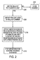
- FIG. 2 is a flow chart illustrating the processing steps in accordance with one embodiment of the present invention.
- FIG. 3 is an x-ray diffractometer plot of the amorphous silicon film manufactured in accordance with one embodiment of the present invention.
- FIGS. 4 is an infrared spectrum plot of the amorphous silicon film manufactured in accordance with one embodiment of the present invention.
- FIG. 5 illustrates a density of states versus the depth in energy from the conduction edge of the bandgap plot of an amorphous silicon film manufactured in accordance with the processing method of the present invention.
- FIG. 6 is a photocapacitance versus photon energy graph of an amorphous silicon film manufactured in accordance with the processing method of the present invention.
- the inventors of the present invention have identified the following three factors that contribute to the problems encountered with the various prior art approaches to forming a-Si:H films at high deposition rates.
- these prior art approaches utilize low flow rates of silicon-containing precursors into the chamber, thereby increasing the number and rate of particles generated in the process chamber.
- the present invention provides a high deposition rate method for forming a-Si:H films and a resulting a-Si:H film that exhibits a low defect density.
- the present invention provides novel techniques and mechanisms to (1) reduce the number of particles generated in the chamber; and (2) to remove particles that have been generated in the chamber.
- the present invention reduces the number of particles generated in the chamber by defining a novel processing parameter and enforcing the parameter in the process.
- This processing parameter relates to the plasma in the chamber and the flow rate of the gas provided into the chamber.
- the present invention defines a plasma volume in the chamber.
- the present invention defines a flow rate of the gas entering the chamber.
- the present invention specifies a process parameter (K) that defines a predetermined relationship between the plasma volume to pumping speed.
- the predetermined relationship can be the ratio between the plasma volume and the pumping speed (e.g., the flow rate of the gas).
- the processing method of the present invention specifies a high flow rate of silicon-containing precursors with a low partial pressure of these silicon-containing precursors. Furthermore, the processing method of the present invention specifies a high plasma power to fragment the silicon-containing precursors efficiently. Last, the temperature of the wafer, the amount of hydrogen in the chamber, and the amount of hydrogen in the film are controlled by the present invention in order to produce a-Si:H material or film with minimum defect density.
- the present invention also teaches the removal of particles generated in the chamber.
- the removal of particles can be accomplished by utilizing a process chamber that can be easily and readily cleaned or by using a self-cleaning chamber.
- FIG. 1 there is shown a schematic sectional view of a plasma-enhanced chemical vapor deposition (PECVD) apparatus 10 (referred to herein also as a plasma reactor 10) in which the method in accordance with the present invention can be performed.
- the apparatus 10 has a deposition chamber 12 which includes a top wall 14, side walls 32 and a bottom wall 22.
- the top wall 12 defines an opening therethrough.
- the apparatus 10 also has a first electrode or a gas inlet manifold 16 within the opening defined by the top wall 12.
- the top wall 14 can be solid with the electrode 16 being adjacent to the inner surface thereof.
- Within chamber 12 is a susceptor 18 in the form of a plate which extends parallel to the first electrode 16.
- the susceptor 18 can be connected to ground so that it serves as a second electrode.
- the susceptor 18 is mounted on the end of a shaft 20 which extends vertically through the bottom wall 22 of the deposition chamber 12.
- the shaft 20 is movable vertically so as to permit the movement of the susceptor 18 vertically toward and away from the first electrode 16.
- a gas outlet 30 extends through the side wall 32 of the deposition chamber 12 and is connected to means (not shown) for evacuating the deposition chamber 12.
- a gas inlet pipe 42 extends through the first electrode or the gas inlet manifold 16 of the deposition chamber 12, and is connected through a gas switching network (not shown) to sources (not shown) of various gases. It is noted that more than one gas inlet 42 may be employed, and the gas inlet 42 may extend through one of the other walls of the chamber 12.
- the first electrode 16 is connected to an RF power source 36.
- a substrate 38 (e.g., a silicon substrate) is first loaded into the deposition chamber 12 and is placed on the susceptor 18 by the transfer plate (not shown).
- a commonly used size for a silicon transistor substrate is approximately 100 mm by 300 mm.
- the susceptor 18 lifts the substrate 38 to position the substrate 38 relatively close to the first electrode 16.
- the preferred electrode spacing or the distance between the substrate surface and the discharge surface of the gas inlet manifold 16 is between about 250 to about 800 mils.
- FIG. 2 is a flow chart illustrating the processing steps in accordance with one embodiment of the present invention.
- the deposition chamber 12 is first evacuated through the gas outlet 30.
- step 200 a determination is made whether the walls of the chamber 12 are clean (e.g., do the walls have an unacceptable level of impurities).
- This level of impurities is predetermined and can vary across different processes and applications. Preferably, the level of impurities is limited to less than 10 15 /cm 3 or below the detectability by SIMS for most applications.
- impurities can include silicon residue or dopants (e.g., phosphorous, boron, aluminum, or arsenic).
- One such impurity detection method is to utilize secondary ion mass spectroscopy (SIMS).
- SIMS secondary ion mass spectroscopy
- Another impurity detection method is to grow some film on the wall and examine the impurities therein.
- step 204 the walls of the chamber 12 are cleaned. After the cleaning step, processing then proceeds to step 208. If in step 200, it is determined that the level of impurities is at an acceptable level, the processing proceeds directly to step 208 without cleaning step 204.
- the processing chamber can self-clean without leaving particles behind.
- An in-situ cleaning process of the interior of the chamber can be carried out after each deposition, when changing dopant type, or when particle generation may be at issue.
- the cleaning process effectively removes the contaminants and particles from the chamber walls that can be the source of unwanted impurities in the film.
- the frequency of such in-situ cleaning depends on many processing parameters which are determined in each deposition process.
- a vacuum system can be coupled to the chamber to allow for vacuum transfer of wafers to a holding area so that the chamber may be cleaned without the wafer in it.
- the wafer can be moved in and out of the chamber several times.
- a pre-coat layer optionally can be deposited on the walls of the chamber 12. It is important to note that the wafer or substrate is not in the chamber 12 at this point in the process.
- the pre-coat layer which can be a SiN film or SiO 2 film, is deposited on the walls of the chamber 12 by utilizing techniques that are well known in the art. For example, the introduction of nitrous oxide and silane through a plasma is effective for creating a SiO 2 film on the walls of the chamber 12. Similarly, the introduction of silane with nitrogen and/or ammonia through a plasma is effective for creating a SiN film on the walls of the chamber 12.
- a substrate 38 e.g., a silicon substrate
- amorphous silicon is deposited while maintaining a process parameter (K) in a predetermined relationship between a predetermined value.
- the process parameter (K) can include a plasma volume and a flow rate of gas into the chamber 12.
- the deposition can be performed by creating a plasma with the plasma volume in the chamber subject to a process parameter (K).
- the process parameter (K) is a ratio of the plasma volume to the total flow rate of the mixture of gases, and the process parameter is maintained in a first predetermined relationship with a first predetermined ratio.
- Creating a plasma in the chamber 12 can include introducing gas, which can include a reactant gas and an inert gas into the chamber 12 at a total flow rate that is subject to the process parameter (K) (e.g., a plasma volume-to-flow rate ratio) and allowing the flow rate to stabilize.
- the flow rate is the sum of the flow rates of all gases in the mixture 56 of gas.
- the flow rate is given in units of "sccm", which stands for "standard cubic centimeter per minute".
- standard temperature and pressure (STP) is 298°K at 1 atm.
- the reactant gas is a silicon-containing pre-cursor, that can be, but is not limited to, silane, disilane, trisilane, other halogenated silane, florinated silane, or dichlorosilane.
- the flow rate of the inert gas is maintained at a high level in order to (1) move the silicon pre-cursor quickly through the plasma volume 50 to increase the silicon deposition rate, and (2) dilute the silicon pre-cursor.
- the inert gas is one of the noble gases, such as helium (He), neon (Ne), argon (Ar), krypton (Kr), or xenon (Xe).
- the step of creating a plasma also includes the step of applying power to the first electrode 16 to create the plasma near the wafer.
- the plasma has a plasma volume 50 that can be controlled by the amount of power applied. It is noted that the plasma is localized in the chamber and not diffuse.
- One method to determine the plasma volume 50 in a two parallel plate configuration is by visual inspection of the glow of the plasma and how far it extends in the chamber 12. The visually derived dimensions can then be utilized to calculate an estimate of the plasma volume 50. It is noted that other methods can be utilized and may be more suited for certain configurations.
- the power density is the amount of power applied divided by the area of the electrode over which the power is applied.
- the power density is preferably in the range of about 0.2 W/cm 2 to about 1 W/cm 2 , but may be higher in other configurations. It is noted that in this case the power density employed by the present invention is much higher (about an order of magnitude higher) than conventional power density measures which typically range from 0.01 W/cm 2 to about 0.1 W/cm 2 .
- the power can be first applied to the first electrode 16 and then the gas can be introduced into the chamber 12 to create a plasma or vis-versa.
- a process parameter (K) e.g., a plasma volume to flow rate ratio
- K a plasma volume to flow rate ratio
- the mean transit time is the average time needed for a gas molecule to travel through the plasma region (e.g., the region from the injector to outside the glow region).
- the mean transit time for the process of the present invention is less than 1.5s. In one embodiment, the mean transit time of approximately 0.5s provides good process results.
- the deposition is stopped after a desired film thickness is achieved.
- the plasma can be stopped by shutting off the power after a particular thickness of the a-Si:H is achieved.
- an alternative way to stop the plasma is to shut off the supply of reactant gas (e.g., the silicon containing precursor).
- the deposition rate is known, after a predetermined amount of time, the deposition can be stopped.
- a measuring device such as a deposition rate monitor, can be employed to measure the thickness of the a-Si:H film, and the power can be shut-off after a predetermined thickness has been achieved.
- a quartz balance can be utilized for measuring the thickness of the a-Si:H film.
- the chamber 12 can be vented, and the wafer removed from the chamber 12.
- the wafer can be transferred directly to an evacuated chamber for further processing after step 218.
- high quality a-Si:H films are achieved by depositing gas (e.g., a mixture of silicon pre-cursor and inert gas) while maintaining the pressure in the CVD chamber at between about 2 to about 9 Torr, and the substrate setpoint temperature at about 225 degrees to 330 degrees Celsius.
- gas e.g., a mixture of silicon pre-cursor and inert gas
- the actual temperature of the substrate is different from the setpoint temperature and typically may be about 30 degrees less than the setpoint temperature.
- a preferred way to establish the deposition temperature is to grow material or film at several different temperatures and obtain an infrared spectrum plot (e.g., the FTIR spectrum plot of FIG. 4). Referring to FIG. 4, the temperature is determined by maximizing the amount of total hydrogen, but at the same time minimizing the shoulder or peak at 2100 cm -1 .
- Gas flow rates are regulated to maintain adequate reactant gas levels and in accordance with the processing parameter (K) that relates plasma volume with the flow rate.
- K processing parameter
- silane at between 150 and 300 sccm and Argon at between 3000 and 7000 sccm are employed to deposit a-Si:H film on the substrate.
- a suitable thickness of the a-Si:H film is between about 10 nm to 2000 nm.
- the preferred processing conditions for the deposition of the a-Si:H film is shown below in Table I.
- the gas spends a minimum time in the plasma, thereby decreasing the formation of particles that may fall onto the silicon wafer or attach onto the walls of the chamber.
- the deposition rate (also referred to herein as the "dep. rate”) is usually proportional to the flow rate (Q).
- the dep. rate In the prior art, it was thought that in order to deposit a high quality material, the dep. rate had to be kept low. Since the dep. rate is usually proportional to the flow rate (Q), it was thought that in order to deposit a high quality amorphous silicon layer, the flow rate (Q) must be kept low as well.
- the present invention increases the flow rate (Q), thereby increasing the deposition rate while maintaining the quality of the resultant product.
- the present invention increases the pumping speed (S) as well.
- the other steps of the method of the present invention such as a localized low-energy plasma and cleaning of the chamber, address the particle generation issue, and produce a high quality layer of amorphous silicon.
- the a-Si:H film that is produced by the process of the present invention has a deposition rate of at least 25 Angstroms per second across the wafer and has a defect density of no more than 1.3 x 10 16 cm -3 . It is noted that defect densities of 2 x 10 15 cm -3 to 3 x 10 15 cm -3 may be achieved by the process of the present invention. Also, deposition rates of 30 to 40 Angstroms per second have been achieved by the present invention. It is believed that as higher pumping speeds are utilized, the defect density can be further reduced.
- the amorphous silicon film is deposited by a chemical vapor deposition process conducted at a high deposition rate being selected from the respective range of between 25 and 40 Angstroms/s.
- the processing method of the present invention specifies a small plasma volume to pumping speed ratio, utilizes a CVD chamber that can be easily and readily cleaned, specifies a high flow rate of silicon-containing precursors with a low partial pressure of these silicon-containing precursors, and specifies a high plasma power to fragment the silicon-containing precursors efficiently.
- non-doped amorphous silicon is equally applicable to doped films of amorphous silicon.
- doped amorphous silicon e.g., diborane or phosphine
- the processing equipment can include a mechanism to flow controlled amounts of gases containing dopant atoms to be incorporated in the doped film.
- dopants include, but are not limited to, the following: B, Al, Ga, In, C, Sn , Ge, Pb, P, N, As, Sb, Ti, Bi, Se, S, Te, and O.
- the doped silicon film can then be made under similar process conditions as described above with the addition of small amounts of dopant.
- the hydrogenated amorphous silicon manufactured in accordance with one embodiment of the present invention can be identified by utilizing one or more measurements of the properties of the hydrogenated amorphous silicon. These properties are now described with reference to FIGS. 3-6.
- FIG. 3 is an x-ray diffractometer plot of the hydrogenated amorphous silicon manufactured in accordance with one embodiment of the present invention.
- the measurement set-up to obtain this plot is well-known by those of ordinary skill in the art and includes an x-ray source for generating and directing an x-ray beam at a sample (i.e., material under measurement) and a detector positioned to receive x-rays that are diffracted from the sample.
- the vertical axis represents a relative intensity that may be expressed in any arbitrary units. The intensity is a relative measure of the number of x-rays that received by the detector.
- the horizontal axis represents the angle formed by the incoming x-ray beam and the x-ray beam diffracted by the sample.
- the angle is given in units of two-theta. It is noted that there is a peak 310 at approximate 27 degrees, and a harmonic 320 thereof at approximately 54 degrees, which is one unique signature of the amorphous silicon layer deposited by the method of the present invention.
- the peak 310 represents the amorphous band that shows scattering based on average Si-Si atom spacing. The x-ray diffractometry does not detect a significant fraction of crystalline material.
- FIG. 4 is an infrared spectrum plot of the hydrogenated amorphous silicon manufactured in accordance with one embodiment of the present invention.
- the measurement set-up to obtain this plot is well-known by those of ordinary skill in the art and includes an infrared source for generating and directing an infrared light at a sample (i.e., the material under measurement) and a detector positioned to receive infrared light that passes through the sample.
- the horizontal axis represents a wave number, which is a relative measure that simply is the inverse of the wavelength of the incident infrared light.
- the vertical axis represents the absorbance (i.e., a measure of the amount of light that does not pass through the material.
- FIG. 4 illustrates five curves that correspond to five different temperatures.
- a first curve 400 corresponds to 3.00 degrees Celsius.
- a second curve 402 corresponds to 275 degrees Celsius.
- a third curve 404 corresponds to 250 degrees Celsius.
- a fourth curve 406 corresponds to 225 degrees Celsius.
- a fifth curve 408 corresponds to 200 degrees Celsius.
- the first curve 400 and the second curve 402 exhibit a slight shoulder at approximately 2100 cm -1 .
- the number of hydrogen atoms can be increased or decreased to achieve an optimal number of hydrogen atoms.
- the optimal condition is when the number of hydrogen atoms closely matches the number of dangling bonds in the silicon.
- the infrared spectrum plot exhibits a shoulder (e.g., curves 400 and 402).
- the a-Si:H material of the present invention features an infrared spectrum plot of either the fourth curve 406 (225 degrees Celsius) or the fifth curve 408 (200 degrees Celsius) that both do not exhibit a shoulder, thereby indicating that the number of hydrogen atoms closely matches the number needed to bond with the dangling bonds of the silicon.
- the preferred manner of determining the process temperature is through the use of infrared spectrum plot of FIG. 4.
- the a-Si:H deposited film manufactured by the processing method of the present invention has a smooth and glassy appearance when viewed at 50,000x magnification on a scanning electron microscope (SEM).
- SEM scanning electron microscope
- the cross sectional view and plan view of the a-Si:H deposited film manufactured by the processing method of the present invention reveal a void-free morphology.
- FIG. 5 illustrates a density of states versus the depth in energy from the conduction edge of the bandgap plot (referred to herein as the density of states plot) of the hydrogenated amorphous silicon manufactured in accordance with one embodiment of the present invention.
- This density of states plot provides a fingerprint of the hydrogenated amorphous silicon of the present invention.
- the density of states plot indicates the quality of the material and generally reveals the extent of leakage of devices that are manufacture in the film. This plot also indicates the extent of dangling bond defects, which can contribute to leakage, and is an indicator of quality of the material. It is noted that the integrated DOS is less than about 6 x 10 15 cm -3 .
- the thermal carrier generation activation energy (E a ) is about 0.9eV
- the Urbach energy (E U ) is about 56meV.
- FIG. 6 is a photocapacitance versus photon energy graph of the hydrogenated amorphous silicon manufactured in accordance with one embodiment of the present invention.
- the slope 604 of the straight portion 608 of the curve represents density of states (DOS) along the valence band edge.
- the slope 604 and the shoulder 612 that is defined between approximately 0.8eV and 1.4eV provide a signature of a-Si:H film manufactured by the process of the present invention.
- the slope 604 of the steep portion of the a-Si:H film manufactured by the process of the present invention indicates that the film has more order in the atomic structure of the film than a material having a higher slope.
- the increased order improves mobility (i.e., there is less stored charge), thereby lowering the capacitance in the film.
- the faster devices manufactured therein exhibit a faster response (i.e., the speed of the devices increases).
- the slope of the steep portion is about 56 meV.
- low quality materials have a much higher slope of about 70 to 80 meV indicating greater disorder.
- FIGS. 3 to 6 These plots or graphs provide a unique signature of the a-Si:H so that when these measurements are taken for a given sample material, a determination may be made whether the sample material is the a-Si:H manufactured by the process of the present invention.
Landscapes
- Chemical & Material Sciences (AREA)
- Engineering & Computer Science (AREA)
- Materials Engineering (AREA)
- General Chemical & Material Sciences (AREA)
- Chemical Kinetics & Catalysis (AREA)
- Mechanical Engineering (AREA)
- Metallurgy (AREA)
- Organic Chemistry (AREA)
- Plasma & Fusion (AREA)
- Physics & Mathematics (AREA)
- Inorganic Chemistry (AREA)
- Chemical Vapour Deposition (AREA)
- Photovoltaic Devices (AREA)
Applications Claiming Priority (2)
| Application Number | Priority Date | Filing Date | Title |
|---|---|---|---|
| US591815 | 1990-10-02 | ||
| US09/591,815 US6436488B1 (en) | 2000-06-12 | 2000-06-12 | Chemical vapor deposition method for amorphous silicon and resulting film |
Publications (3)
| Publication Number | Publication Date |
|---|---|
| EP1164206A2 true EP1164206A2 (fr) | 2001-12-19 |
| EP1164206A3 EP1164206A3 (fr) | 2003-11-05 |
| EP1164206B1 EP1164206B1 (fr) | 2006-11-15 |
Family
ID=24368059
Family Applications (1)
| Application Number | Title | Priority Date | Filing Date |
|---|---|---|---|
| EP01108183A Expired - Lifetime EP1164206B1 (fr) | 2000-06-12 | 2001-03-30 | Procédé cvd pour la production de silicium amorphe |
Country Status (6)
| Country | Link |
|---|---|
| US (1) | US6436488B1 (fr) |
| EP (1) | EP1164206B1 (fr) |
| JP (1) | JP2002047568A (fr) |
| KR (1) | KR100762063B1 (fr) |
| CN (2) | CN1238555C (fr) |
| DE (1) | DE60124452T2 (fr) |
Cited By (4)
| Publication number | Priority date | Publication date | Assignee | Title |
|---|---|---|---|---|
| WO2004088710A3 (fr) * | 2003-04-02 | 2005-12-08 | Nkt Res & Innovation As | Procede et appareil de traitement au plasma gazeux a longueur controlee de plasma gazeux et utilisation correspondante |
| EP1524703A3 (fr) * | 2003-10-17 | 2007-10-10 | Sharp Kabushiki Kaisha | Procédé de fabrication d'une cellule solaire à base de Si |
| WO2010054164A3 (fr) * | 2008-11-07 | 2010-07-29 | United Solar Ovonic Llc | Matériau semi-conducteur de grande qualité |
| CN110970287A (zh) * | 2018-09-28 | 2020-04-07 | 长鑫存储技术有限公司 | 制备非晶硅薄膜的方法 |
Families Citing this family (14)
| Publication number | Priority date | Publication date | Assignee | Title |
|---|---|---|---|---|
| US6786968B2 (en) * | 2002-10-31 | 2004-09-07 | Agilent Technologies, Inc. | Method for low temperature photonic crystal structures |
| US6747773B2 (en) * | 2002-10-31 | 2004-06-08 | Agilent Technologies, Inc. | Method and structure for stub tunable resonant cavity for photonic crystals |
| US20100147379A1 (en) * | 2005-10-03 | 2010-06-17 | Katsushi Kishimoto | Silicon-based thin-film photoelectric conversion device, and method and apparatus for manufacturing the same |
| US20100178017A1 (en) * | 2006-10-06 | 2010-07-15 | Boris Kharas | Method for Improving Refractive Index Control in PECVD Deposited a-SiNy Films |
| KR20100033091A (ko) * | 2008-09-19 | 2010-03-29 | 한국전자통신연구원 | 화학기상증착법에 의한 비정질 실리콘 박막의 증착방법 |
| JP5793398B2 (ja) * | 2011-10-28 | 2015-10-14 | 東京エレクトロン株式会社 | シード層の形成方法及びシリコン含有薄膜の成膜方法 |
| CN102637780B (zh) * | 2012-04-27 | 2014-04-02 | 保定天威薄膜光伏有限公司 | 一种提高产业化硅薄膜电池组件性能的制备方法 |
| CN103774116B (zh) * | 2012-10-19 | 2016-09-21 | 陕西拓日新能源科技有限公司 | 用于非晶硅电池沉积的等离子体气相沉积设备与方法 |
| KR101489306B1 (ko) * | 2013-10-21 | 2015-02-11 | 주식회사 유진테크 | 어모퍼스 실리콘막의 증착 방법 및 증착 장치 |
| CN104681639A (zh) * | 2013-12-02 | 2015-06-03 | 北京有色金属研究总院 | 一种基于柔性基底的多晶硅薄膜太阳能电池及其制备方法 |
| CN104152864B (zh) * | 2014-08-22 | 2016-11-16 | 中国科学院宁波材料技术与工程研究所 | 硅薄膜的制备方法 |
| CN109935640B (zh) * | 2019-04-02 | 2021-11-05 | 江苏微导纳米科技股份有限公司 | 一种晶体硅太阳能电池的镀膜方法 |
| CN110779849B (zh) * | 2019-12-05 | 2022-05-03 | 成都中医药大学 | 一种非晶态二氧化硅比表面积的测定方法 |
| CN112481606A (zh) * | 2020-11-10 | 2021-03-12 | 江苏杰太光电技术有限公司 | 一种pecvd沉积太阳能电池掺杂层的气源和系统 |
Family Cites Families (12)
| Publication number | Priority date | Publication date | Assignee | Title |
|---|---|---|---|---|
| DE3429899A1 (de) * | 1983-08-16 | 1985-03-07 | Canon K.K., Tokio/Tokyo | Verfahren zur bildung eines abscheidungsfilms |
| US4792460A (en) * | 1986-07-15 | 1988-12-20 | Electric Power Research Institute, Inc. | Method for production of polysilanes and polygermanes, and deposition of hydrogenated amorphous silicon, alloys thereof, or hydrogenated amorphous germanium |
| US5126169A (en) * | 1986-08-28 | 1992-06-30 | Canon Kabushiki Kaisha | Process for forming a deposited film from two mutually reactive active species |
| US5082696A (en) * | 1986-10-03 | 1992-01-21 | Dow Corning Corporation | Method of forming semiconducting amorphous silicon films from the thermal decomposition of dihalosilanes |
| US5338580A (en) * | 1988-11-15 | 1994-08-16 | Canon Kabushiki Kaisha | Method of preparation of functional deposited film by microwave plasma chemical vapor deposition |
| US5324360A (en) * | 1991-05-21 | 1994-06-28 | Canon Kabushiki Kaisha | Method for producing non-monocrystalline semiconductor device and apparatus therefor |
| US5670224A (en) * | 1992-11-13 | 1997-09-23 | Energy Conversion Devices, Inc. | Modified silicon oxide barrier coatings produced by microwave CVD deposition on polymeric substrates |
| US5648293A (en) | 1993-07-22 | 1997-07-15 | Nec Corporation | Method of growing an amorphous silicon film |
| DE69424759T2 (de) * | 1993-12-28 | 2001-02-08 | Applied Materials, Inc. | Gasphasenabscheidungsverfahren in einer einzigen Kammer für Dünnfilmtransistoren |
| JP3851686B2 (ja) * | 1996-06-08 | 2006-11-29 | キヤノンアネルバ株式会社 | プラズマcvdによる薄膜形成方法 |
| KR19980055934A (ko) * | 1996-12-28 | 1998-09-25 | 김영환 | 반도체 소자의 층간 절연막 |
| AUPP055497A0 (en) * | 1997-11-26 | 1997-12-18 | Pacific Solar Pty Limited | High rate deposition of amorphous silicon films |
-
2000
- 2000-06-12 US US09/591,815 patent/US6436488B1/en not_active Expired - Lifetime
-
2001
- 2001-03-30 EP EP01108183A patent/EP1164206B1/fr not_active Expired - Lifetime
- 2001-03-30 DE DE60124452T patent/DE60124452T2/de not_active Expired - Fee Related
- 2001-06-11 KR KR1020010032585A patent/KR100762063B1/ko not_active Expired - Fee Related
- 2001-06-12 CN CNB01121189XA patent/CN1238555C/zh not_active Expired - Fee Related
- 2001-06-12 CN CNB2005100559064A patent/CN100557076C/zh not_active Expired - Fee Related
- 2001-06-12 JP JP2001176532A patent/JP2002047568A/ja active Pending
Cited By (4)
| Publication number | Priority date | Publication date | Assignee | Title |
|---|---|---|---|---|
| WO2004088710A3 (fr) * | 2003-04-02 | 2005-12-08 | Nkt Res & Innovation As | Procede et appareil de traitement au plasma gazeux a longueur controlee de plasma gazeux et utilisation correspondante |
| EP1524703A3 (fr) * | 2003-10-17 | 2007-10-10 | Sharp Kabushiki Kaisha | Procédé de fabrication d'une cellule solaire à base de Si |
| WO2010054164A3 (fr) * | 2008-11-07 | 2010-07-29 | United Solar Ovonic Llc | Matériau semi-conducteur de grande qualité |
| CN110970287A (zh) * | 2018-09-28 | 2020-04-07 | 长鑫存储技术有限公司 | 制备非晶硅薄膜的方法 |
Also Published As
| Publication number | Publication date |
|---|---|
| CN1657648A (zh) | 2005-08-24 |
| EP1164206B1 (fr) | 2006-11-15 |
| JP2002047568A (ja) | 2002-02-15 |
| CN1238555C (zh) | 2006-01-25 |
| KR20010111632A (ko) | 2001-12-19 |
| DE60124452T2 (de) | 2007-03-15 |
| CN100557076C (zh) | 2009-11-04 |
| KR100762063B1 (ko) | 2007-10-01 |
| CN1339617A (zh) | 2002-03-13 |
| EP1164206A3 (fr) | 2003-11-05 |
| DE60124452D1 (de) | 2006-12-28 |
| US6436488B1 (en) | 2002-08-20 |
Similar Documents
| Publication | Publication Date | Title |
|---|---|---|
| US6436488B1 (en) | Chemical vapor deposition method for amorphous silicon and resulting film | |
| KR101050377B1 (ko) | 반도체 박막 증착을 위한 개선된 공정 | |
| US5632821A (en) | Post treatment method for in-situ cleaning | |
| US20040033674A1 (en) | Deposition of amorphous silicon-containing films | |
| US20090142878A1 (en) | Plasma treatment between deposition processes | |
| US7943463B2 (en) | Methods of semiconductor processing involving forming doped polysilicon on undoped polysilicon | |
| KR20080016988A (ko) | Cvd를 이용한 치환형 탄소가 높게 도핑된 결정질 실리콘층의 제조 방법 | |
| EP0488112B1 (fr) | Procédé de fabrication d'une couche mince de silicium amorphe, par dépôt chimique en phase vapeur assisté par un plasma | |
| Nunomura et al. | Precursor flux-dependent microstructure of thin-film silicon prepared by hydrogen diluted silane discharge plasmas | |
| JP3606426B2 (ja) | 堆積膜形成方法及び堆積膜形成装置 | |
| JPH04342121A (ja) | 水素化非晶質シリコン薄膜の製造方法 | |
| Hapke et al. | Structural investigation and growth of< n>-type microcrystalline silicon prepared at different plasma excitation frequencies | |
| Zhang et al. | Silicon‐based narrow‐bandgap thin‐film semiconductor materials: polycrystalline SiGe prepared by reactive thermal CVD | |
| JP3024543B2 (ja) | 結晶性シリコン膜及びその製造方法 | |
| Lin et al. | Low-temperature growth of poly-crystalline silicon films using SiCl/sub 4/and H/sub 2/mixture | |
| Oh et al. | Growth of very low temperature polysilicon film by remote plasma-enhanced chemical-vapor deposition | |
| Flückiger | Microcrystalline silicon thin films deposited by VHF plasmas for solar cells applications | |
| Sawado et al. | Contributions of Silicon-Hydride Radicals to Hydrogenated Amorphous Silicon Film Formation in Windowless Photochemical Vapor Deposition System | |
| Kakiuchi et al. | High-rate and low-temperature film growth technology using stable glow plasma at atmospheric pressure | |
| Boldyryeva et al. | Characterization of hydrogen contained in passivated poly‐Si and microcrystalline‐Si by ERDA technique | |
| Tsuchida et al. | Structure of Polycrystalline Silicon Films by Glow-Discharge Decomposition using SiH4/H2/SiF4 at Low Temperature | |
| JP2000232073A (ja) | 多結晶シリコン膜 | |
| Wank et al. | Manipulating the hydrogen-bonding configuration in ETP-CVD a-Si: H | |
| Okitsu et al. | Electron Beam Excited Plasma CVD for Silicon Growth | |
| Chae et al. | Evaluation of Microcrystalline Silicon Films Deposited by Ultrafast Thermal Plasma CVD |
Legal Events
| Date | Code | Title | Description |
|---|---|---|---|
| PUAI | Public reference made under article 153(3) epc to a published international application that has entered the european phase |
Free format text: ORIGINAL CODE: 0009012 |
|
| AK | Designated contracting states |
Kind code of ref document: A2 Designated state(s): AT BE CH CY DE DK ES FI FR GB GR IE IT LI LU MC NL PT SE TR |
|
| AX | Request for extension of the european patent |
Free format text: AL;LT;LV;MK;RO;SI |
|
| PUAL | Search report despatched |
Free format text: ORIGINAL CODE: 0009013 |
|
| AK | Designated contracting states |
Kind code of ref document: A3 Designated state(s): AT BE CH CY DE DK ES FI FR GB GR IE IT LI LU MC NL PT SE TR |
|
| AX | Request for extension of the european patent |
Extension state: AL LT LV MK RO SI |
|
| 17P | Request for examination filed |
Effective date: 20040430 |
|
| AKX | Designation fees paid |
Designated state(s): DE FR GB IT NL |
|
| GRAP | Despatch of communication of intention to grant a patent |
Free format text: ORIGINAL CODE: EPIDOSNIGR1 |
|
| RTI1 | Title (correction) |
Free format text: CHEMICAL VAPOR DEPOSITION METHOD FOR AMORPHOUS SILICON |
|
| GRAS | Grant fee paid |
Free format text: ORIGINAL CODE: EPIDOSNIGR3 |
|
| GRAA | (expected) grant |
Free format text: ORIGINAL CODE: 0009210 |
|
| AK | Designated contracting states |
Kind code of ref document: B1 Designated state(s): DE FR GB IT NL |
|
| REG | Reference to a national code |
Ref country code: GB Ref legal event code: FG4D |
|
| RAP2 | Party data changed (patent owner data changed or rights of a patent transferred) |
Owner name: AVAGO TECHNOLOGIES GENERAL IP (SINGAPORE) PTE. LTD |
|
| REF | Corresponds to: |
Ref document number: 60124452 Country of ref document: DE Date of ref document: 20061228 Kind code of ref document: P |
|
| NLT2 | Nl: modifications (of names), taken from the european patent patent bulletin |
Owner name: AVAGO TECHNOLOGIES GENERAL IP (SINGAPORE) PTE. LTD Effective date: 20061227 |
|
| REG | Reference to a national code |
Ref country code: GB Ref legal event code: 732E |
|
| ET | Fr: translation filed | ||
| PGFP | Annual fee paid to national office [announced via postgrant information from national office to epo] |
Ref country code: DE Payment date: 20070430 Year of fee payment: 7 |
|
| PLBE | No opposition filed within time limit |
Free format text: ORIGINAL CODE: 0009261 |
|
| STAA | Information on the status of an ep patent application or granted ep patent |
Free format text: STATUS: NO OPPOSITION FILED WITHIN TIME LIMIT |
|
| 26N | No opposition filed |
Effective date: 20070817 |
|
| NLV4 | Nl: lapsed or anulled due to non-payment of the annual fee |
Effective date: 20071001 |
|
| REG | Reference to a national code |
Ref country code: FR Ref legal event code: ST Effective date: 20071130 |
|
| PG25 | Lapsed in a contracting state [announced via postgrant information from national office to epo] |
Ref country code: NL Free format text: LAPSE BECAUSE OF NON-PAYMENT OF DUE FEES Effective date: 20071001 |
|
| PG25 | Lapsed in a contracting state [announced via postgrant information from national office to epo] |
Ref country code: FR Free format text: LAPSE BECAUSE OF NON-PAYMENT OF DUE FEES Effective date: 20070402 |
|
| PG25 | Lapsed in a contracting state [announced via postgrant information from national office to epo] |
Ref country code: DE Free format text: LAPSE BECAUSE OF NON-PAYMENT OF DUE FEES Effective date: 20081001 |
|
| PG25 | Lapsed in a contracting state [announced via postgrant information from national office to epo] |
Ref country code: IT Free format text: LAPSE BECAUSE OF NON-PAYMENT OF DUE FEES Effective date: 20070330 |
|
| PGFP | Annual fee paid to national office [announced via postgrant information from national office to epo] |
Ref country code: GB Payment date: 20100322 Year of fee payment: 10 |
|
| GBPC | Gb: european patent ceased through non-payment of renewal fee |
Effective date: 20110330 |
|
| PG25 | Lapsed in a contracting state [announced via postgrant information from national office to epo] |
Ref country code: GB Free format text: LAPSE BECAUSE OF NON-PAYMENT OF DUE FEES Effective date: 20110330 |