EP1164707A2 - Verfahren zur Dämpfung unerwünchten Frequenzen während der Abtastung eines Nachrichtensignals - Google Patents
Verfahren zur Dämpfung unerwünchten Frequenzen während der Abtastung eines Nachrichtensignals Download PDFInfo
- Publication number
- EP1164707A2 EP1164707A2 EP01000143A EP01000143A EP1164707A2 EP 1164707 A2 EP1164707 A2 EP 1164707A2 EP 01000143 A EP01000143 A EP 01000143A EP 01000143 A EP01000143 A EP 01000143A EP 1164707 A2 EP1164707 A2 EP 1164707A2
- Authority
- EP
- European Patent Office
- Prior art keywords
- signal
- analog signal
- capacitor
- filter
- coupled
- Prior art date
- Legal status (The legal status is an assumption and is not a legal conclusion. Google has not performed a legal analysis and makes no representation as to the accuracy of the status listed.)
- Granted
Links
Images



Classifications
-
- H—ELECTRICITY
- H03—ELECTRONIC CIRCUITRY
- H03M—CODING; DECODING; CODE CONVERSION IN GENERAL
- H03M1/00—Analogue/digital conversion; Digital/analogue conversion
- H03M1/06—Continuously compensating for, or preventing, undesired influence of physical parameters
- H03M1/0617—Continuously compensating for, or preventing, undesired influence of physical parameters characterised by the use of methods or means not specific to a particular type of detrimental influence
- H03M1/0626—Continuously compensating for, or preventing, undesired influence of physical parameters characterised by the use of methods or means not specific to a particular type of detrimental influence by filtering
-
- H—ELECTRICITY
- H03—ELECTRONIC CIRCUITRY
- H03M—CODING; DECODING; CODE CONVERSION IN GENERAL
- H03M3/00—Conversion of analogue values to or from differential modulation
- H03M3/30—Delta-sigma modulation
- H03M3/322—Continuously compensating for, or preventing, undesired influence of physical parameters
- H03M3/324—Continuously compensating for, or preventing, undesired influence of physical parameters characterised by means or methods for compensating or preventing more than one type of error at a time, e.g. by synchronisation or using a ratiometric arrangement
- H03M3/344—Continuously compensating for, or preventing, undesired influence of physical parameters characterised by means or methods for compensating or preventing more than one type of error at a time, e.g. by synchronisation or using a ratiometric arrangement by filtering other than the noise-shaping inherent to delta-sigma modulators, e.g. anti-aliasing
-
- H—ELECTRICITY
- H03—ELECTRONIC CIRCUITRY
- H03M—CODING; DECODING; CODE CONVERSION IN GENERAL
- H03M1/00—Analogue/digital conversion; Digital/analogue conversion
- H03M1/12—Analogue/digital converters
- H03M1/124—Sampling or signal conditioning arrangements specially adapted for A/D converters
- H03M1/1245—Details of sampling arrangements or methods
-
- H—ELECTRICITY
- H03—ELECTRONIC CIRCUITRY
- H03M—CODING; DECODING; CODE CONVERSION IN GENERAL
- H03M3/00—Conversion of analogue values to or from differential modulation
- H03M3/30—Delta-sigma modulation
- H03M3/458—Analogue/digital converters using delta-sigma modulation as an intermediate step
- H03M3/494—Sampling or signal conditioning arrangements specially adapted for delta-sigma type analogue/digital conversion systems
Definitions
- This invention relates generally to frequency channel communications and, more particularly, to attenuation of undesired frequencies in frequency channel communications.
- the energy in the desired frequency channel can be much lower than the energy in adjacent, undesired frequency channels. Accordingly, in order to extract communication signals from the desired frequency channel, communication receiver architectures must address the interference caused by adjacent frequency channels, particularly those of higher energy than the desired frequency channel.
- Some conventional RF receiver architectures such as superheterodyne and direct conversion architectures, utilize high "Q" band-pass SAW filters (channel select filters) to attenuate the interferers.
- SAW filters channel select filters
- Such filters produce a relatively clean channel signal that can then be converted to digital format using conventional low-resolution analog-to-digital converters (ADCs).
- ADCs analog-to-digital converters
- these filters are typically ceramic or crystal electromechanical filters which are disadvantageously large and costly, and which impose an undesirably large signal power loss.
- direct conversion architectures are typically preferred because they permit elimination of SAW filters and hence component count reduction. These architectures also permit the desired channel selection to be performed in the digital domain using digital filters.
- An exemplary direct conversion architecture is illustrated diagrammatically in FIGURE 1.
- the RF communication signal is mixed down at 11, and applied to an anti-aliasing filter at 13.
- the output of the anti-aliasing filter 13 is applied to a high frequency analog-to-digital converter (e.g., a ⁇ modulator) 15.
- the analog-to-digital converter (ADC) works at a selected sampling rate to digitize the entire frequency band including the interferers.
- the interferers are then attenuated by digital filtering at 17.
- the respective signal outputs from each of the components 11, 13, 15 and 17 are also graphically illustrated in FIGURE 1.
- Direct conversion architectures provide high integration capability by trading off analog filter complexity (eliminating the external analog SAW filter) for increases in the oversampling rate and dynamic range of the ADC.
- analog filter complexity eliminating the external analog SAW filter
- dynamic range of the ADC eliminating the external analog SAW filter
- One advantage of this approach is the cost reduction due to elimination of external components, but the drawback is, in general, increased power consumption.
- the increased dynamic range requirement of the ADC is due to the higher interferer energy (relative to the desired signal) caused by the relaxed front-end filter.
- ADC automatic gain control
- the invention incorporates switched capacitor filtering into the process of sampling the analog signal at the input of the ADC. Merging the switched capacitor filter with the ADC advantageously eliminates the need for a large, costly analog filter, while still avoiding complicated ADC design features described above.
- FIGURE 2 diagrammatically illustrates pertinent portions of exemplary embodiments of a communication receiver (e.g., GSM or CDMA) according to the invention.
- a baseband portion of the communication receiver example of FIGURE 2 includes an ADC 23 (e.g. a ⁇ modulator) coupled to receive an analog input from, for example, an anti-aliasing filter such as illustrated at 13 in FIGURE 1.
- the ADC 23 is coupled to a switched capacitor filter bank (or a plurality of such filter banks) at 21.
- the filter bank 21 is also coupled to receive the output of the anti-aliasing filter 13.
- the switched capacitor filter bank 21 is cooperable with the ADC 23 for attenuating interferers in conjunction with the sampling operation of the ADC 23.
- the interfering frequencies have been attenuated by operation of the switched capacitor filter bank 21.
- the signal 24, containing digitized information indicative of the desired communication on the desired frequency channel, is applied to a digital processing section 25 which can process the signal, for example, in any desired conventional manner.
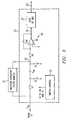
- FIGURE 3 diagrammatically illustrates pertinent portions of exemplary embodiments of the ADC 23 of FIGURE 2.
- FIGURE 3 illustrates one example of a single ended input sampling network for a switched capacitor circuit.
- the switches S1 and S2 are controlled by a switch controller 33 for sampling the analog input signal V IN by storing the associated charge in capacitor C IN .
- Switches S3 and S4 are cooperable under control of the switch controller 33 for dumping the charge stored in capacitor C IN in order to drive an integrator 30 including an operational amplifier 35 and an integrating capacitor C INT .
- the output 36 of the integrator is provided to further portions 37 of the ADC 23. These further portions are well known in the art, and are therefore not explicitly detailed in FIGURE 3.
- the switched capacitor arrangement at S1-S4 and C IN in FIGURE 3 is also conventional (other standard arrangements could also be used), as is the integrator 30.
- the input signal V IN is applied to the switched capacitor filter bank(s) 21 which provide(s) an output signal at a charge summing node 32 of modulator 23.
- FIGURE 4 illustrates an exemplary embodiment of a switched capacitor filter bank 21 according to the invention.
- the filter bank example of FIGURE 4 includes five sections designated generally by K0, K1, K2, K3 and K4. Each of these sections includes an associated pair of switches, S1 K0 and S3 K0 , S1 K1 and S3 K1 , etc.
- Each of the switch pairs of FIGURE 4 corresponds operationally with the switch pair S1 and S3 in FIGURE 3.
- switch S1 K0 of FIGURE 4 cooperates with switch S2 of FIGURE 3 to sample the input signal V IN by storing charge in capacitor C K0 .
- the switch S3 K0 of FIGURE 4 cooperates with the switch S4 of FIGURE 3 for dumping charge from the capacitor C K0 to drive the integrator 30.
- the switch pairs of the remaining sections K1 through K4 of FIGURE 4 also cooperate with switches S2 and S4 of FIGURE 3 to perform sample and dump operations analogous to those described above with respect to section K0.
- the switches of FIGURE 4 are controlled by the switch controller 33 of FIGURE 3 so as to implement a finite impulse response (FIR) filter, for example a filter having the impulse response illustrated in FIGURE 5.
- FIR finite impulse response
- the switch controller 33 controls the switches of FIGURE 4 such that, during each sample and dump cycle performed by switches S1 - S4 of FIGURE 3, one of the switches S1 K0 -S1 K4 of one of the filter sections of FIGURE 4 cooperates with switch S2 of FIGURE 3 to store charge (sample) in its associated capacitor, and one of the switches S3 K0 -S3 K4 of another of the filter sections of FIGURE 4 cooperates with switch S4 of FIGURE 3 to dump charge from its associated capacitor.
- switch S1 K0 of FIGURE 4 also cooperates with switch S2 of FIGURE 3 to sample the input signal V IN at capacitor C K0 .
- switch S3 K1 of FIGURE 4 cooperates with switch S 4 of FIGURE 3 to dump the charge from capacitor C K1 while the charge from capacitor C IN of FIGURE 3 is also being dumped via switches S3 and S4 of FIGURE 3.
- switch S1 K1 of FIGURE 4 cooperates with switch S2 of FIGURE 3 to perform a sample operation with respect to capacitor C K1 .
- switch S3 K2 of FIGURE 4 cooperates with switch S4 of FIGURE 3 to dump the charge from capacitor C K2 .
- switch S1 K2 of FIGURE 4 cooperates with swtich S2 of FIGURE 3 to perform a sample operation with respect to capicitor C K2 .
- switch S3 K3 of FIGURE 4 cooperates with switch S4 of FIGURE 3 to dump the charge from capacitor C K3 .
- switch S1 K3 of FIGURE 4 cooperates with switch S2 of FIGURE 3 to perform a sample operation with respect to capacitor C K3 .
- switch S3 K4 of FIGURE 4 cooperates with switch S4 of FIGURE 3 to dump the charge from capacitor C K4 .
- switch S1 K4 of FIGURE 4 cooperates with switch S2 of FIGURE 3 to perform a sample operation with respect to capacitor C K4 .
- switch S3 K0 of FIGURE 4 cooperates with switch S4 of FIGURE 3 to dump the charge from capacitor C K0 .
- switch S1 K0 of FIGURE 4 again cooperates with switch S2 of FIGURE 3 to perform another sample operation with respect to capacitor C K0 , whereby it can be seen that step (1) above is performed again, and steps (1) - (5) are repeated.
- one or more capacitors can be charged at the same time, and the charge from one or more capacitors can be dumped at the same time during a given dump phase.
- the above-described operation of the filter bank of FIGURE 4 in response to the switch controller 33 causes the charge corresponding to the (i-4)th sample (input that was sampled four clock periods before the current period) to be dumped from a capacitor in FIGURE 4 in parallel with the dumping of the charge corresponding to the ith (current) sample from capacitor C IN of FIGURE 3.
- This operation implements the filter characteristic of FIGURE 5.
- a plurality of filter banks can be provided at 21 in order to provide an FIR filter having any desired number of taps.
- the filter bank(s) at 21 can implement very simple FIRs that can be used to attenuate the desired interferer at the desired frequency. Undesirable phase distortion can be avoided by using linear phase FIR filters, such as illustrated in FIGURE 4.
- the capacitors in the filter bank(s), for example capacitors C K0 - C K4 can of course be scaled to produce the desired filter characteristics. Such capacitor scaling in order to obtain a desired filter characteristic is well known in the art of switched capacitor filter design.
- An automatic gain control (AGC) function can be easily provided, for example, by switching the integrating capacitor C INT in FIGURE 3 from one value to another, thereby effectively scaling the signal. Because this signal scaling occurs after the interferers have been attenuated by the filter at 21, distortion is reduced in the integrator output 36.
- the exemplary bank of capacitors in FIGURE 4 can implement one or more FIR responses, depending on the operation of the switch controller 33 of FIGURE 3. Different FIR responses can implement different filters, or also different scalings of the same filter.
- the FIR filter to be implemented determines which capacitors will be used for sampling and which capacitors will be used for dumping in each cycle.
- the switch controller 33 can be designed to implement the switching sequence necessary to produce the desired FIR response.
- the switched capacitor filter 21 can be designed together with the anti-aliasing filter 13 (see also FIGURE 1) to provide optimization of the overall performance.
- the goal of this optimization is to attenuate the interferers according to the communication channel specifications while minimizing the power consumption in the analog anti-aliasing filter, the FIR filter, and the ADC.
- FIR filters with negative coefficients can be readily obtained in differential implementations by cross-coupling those capacitors which sample the positive input such that they are dumped to the negative summing node, and vice versa.
- FIGURE 6 graphically illustrates the impulse response of an exemplary switched capacitor FIR filter according to the invention.
- the filter characteristic of FIGURE 6 is suitable, for example, for use in a communication receiver in a GSM system.
- FIGURE 7 graphically illustrates the performance associated with the filter characteristic of FIGURE 6.
- the curve at 71 illustrates the performance when only the FIR filter of FIGURE 6 is utilized, and the curve at 72 illustrates the performance when the FIR filter characteristic of FIGURE 6 is combined with a third order anti-aliasing filter.
- the curve 72 demonstrates better than 25 dB rejection of interferers.
- FIGURE 8 graphically illustrates the impulse response of another exemplary switched capacitor FIR filter according to the invention.
- the filter characteristic of FIGURE 8 is suitable, for example, for use in communication receivers operating in WCDMA systems.
- FIGURE 9 graphically illustrates the performance obtained using the filter characteristic of FIGURE 8 with a third order anti-aliasing filter (92) and with the filter of FIGURE 8 only (91).
- FIGURE 10 illustrates exemplary operations which can be performed by the communication receiver embodiments of FIGURES 2-4.
- the analog signal including interferers
- the above-described sampling operation incorporating the filter function for removing the interferers
- the result of the sampling operation is provided (dumped) for conversion to digital format.
- the present invention provides a highly linear, low power technique for filtering out-of-band interferers, while still enabling a fully integrated communication receiver by eliminating external filter components.
- the design complexity of the ADC is reduced as compared to prior art arrangements wherein all of the interferers are converted into digital format and then filtered digitally.
- the invention can utilize a simple, passive FIR switched capacitor network (merged with the functionality of the ADC) with a very small number of non-zero coefficients, and the filter can be optimized to produce band-stop regions in alignment with the most critical interferers.
- ADCs having a dynamic range that is lower by more than 12 to 20 dB relative to ADCs used in direct conversion receivers.
- Such lower dynamic range ADCs have lower size and power requirements, and also require less noise isolation.
- the small number of non-zero coefficients in the FIR filter, and its application at the sampling input of the ADC provide for a simple implementation. It can be shown that simple integer ratios for the non-zero coefficients provides still more reductions in the size and dynamic range required by the ADC.
- the filter can be programmed to meet different band requirements as needed.
Landscapes
- Engineering & Computer Science (AREA)
- Theoretical Computer Science (AREA)
- Filters That Use Time-Delay Elements (AREA)
- Analogue/Digital Conversion (AREA)
- Circuits Of Receivers In General (AREA)
- Compression, Expansion, Code Conversion, And Decoders (AREA)
- Transmission Systems Not Characterized By The Medium Used For Transmission (AREA)
Applications Claiming Priority (2)
| Application Number | Priority Date | Filing Date | Title |
|---|---|---|---|
| US20490200P | 2000-05-15 | 2000-05-15 | |
| US204902P | 2000-05-15 |
Publications (3)
| Publication Number | Publication Date |
|---|---|
| EP1164707A2 true EP1164707A2 (de) | 2001-12-19 |
| EP1164707A3 EP1164707A3 (de) | 2004-12-01 |
| EP1164707B1 EP1164707B1 (de) | 2007-10-24 |
Family
ID=22759956
Family Applications (1)
| Application Number | Title | Priority Date | Filing Date |
|---|---|---|---|
| EP01000143A Expired - Lifetime EP1164707B1 (de) | 2000-05-15 | 2001-05-15 | Verfahren zur Dämpfung unerwünchten Frequenzen während der Abtastung eines Nachrichtensignals |
Country Status (6)
| Country | Link |
|---|---|
| US (1) | US6621441B2 (de) |
| EP (1) | EP1164707B1 (de) |
| JP (1) | JP2002064380A (de) |
| CN (1) | CN1263318C (de) |
| AT (1) | ATE376719T1 (de) |
| DE (1) | DE60131048T2 (de) |
Cited By (3)
| Publication number | Priority date | Publication date | Assignee | Title |
|---|---|---|---|---|
| US6952594B2 (en) | 2002-11-22 | 2005-10-04 | Agilent Technologies, Inc. | Dual-mode RF communication device |
| CN101490956B (zh) * | 2006-10-23 | 2012-02-08 | 松下电器产业株式会社 | 采样滤波器装置以及无线通信装置 |
| CN101331682B (zh) * | 2005-12-13 | 2012-02-08 | 松下电器产业株式会社 | 采样滤波器设备 |
Families Citing this family (16)
| Publication number | Priority date | Publication date | Assignee | Title |
|---|---|---|---|---|
| US6961746B1 (en) * | 2001-06-12 | 2005-11-01 | Analog Devices, Inc. | Current integration circuit with course quantization and small integration capacitor |
| JP4662826B2 (ja) * | 2005-08-05 | 2011-03-30 | 三洋電機株式会社 | スイッチ制御回路、δς変調回路、及びδς変調型adコンバータ |
| KR100828271B1 (ko) * | 2005-08-05 | 2008-05-07 | 산요덴키가부시키가이샤 | 스위치 제어 회로, δ∑ 변조 회로, 및 δ∑ 변조형 ad컨버터 |
| JP5022672B2 (ja) * | 2005-11-22 | 2012-09-12 | パナソニック株式会社 | サンプリングミキサおよび受信機 |
| US8779956B2 (en) * | 2006-12-01 | 2014-07-15 | Intersil Americas Inc. | Sigma-delta converter system and method |
| US7605732B2 (en) * | 2007-01-29 | 2009-10-20 | Texas Instruments Incorporated | Systems and methods for kickback reduction in an ADC |
| US7904048B2 (en) * | 2007-06-29 | 2011-03-08 | Texas Instruments Incorporated | Multi-tap direct sub-sampling mixing system for wireless receivers |
| US7489263B1 (en) | 2007-09-28 | 2009-02-10 | Cirrus Logic, Inc. | Discrete-time programmable-gain analog-to-digital converter (ADC) input circuit with multi-phase reference application |
| US7492296B1 (en) * | 2007-09-28 | 2009-02-17 | Cirrus Logic, Inc. | Discrete-time programmable-gain analog-to-digital converter (ADC) input circuit with input signal and common-mode current nulling |
| US9119572B2 (en) | 2007-10-24 | 2015-09-01 | Josef Gorek | Monitoring trajectory of surgical instrument during the placement of a pedicle screw |
| US8195221B2 (en) * | 2008-06-30 | 2012-06-05 | Intel Corporation | Loop delay compensation for continuous time sigma delta analog to digital converter |
| US8818761B2 (en) * | 2008-08-22 | 2014-08-26 | Nxp B.V. | Device and method for offset compensation based on hysteresis tracking |
| US8768997B2 (en) * | 2009-02-05 | 2014-07-01 | Qualcomm Incorporated | Passive switched-capacitor filters conforming to power constraint |
| EP2477418B1 (de) * | 2011-01-12 | 2014-06-04 | Nxp B.V. | Signalverarbeitungsverfahren |
| US10224757B2 (en) | 2016-12-28 | 2019-03-05 | Texas Instruments Incorporated | Methods and apparatus for antenna signal limiter for radio frequency identification transponder |
| US10038579B1 (en) * | 2017-03-15 | 2018-07-31 | Texas Instruments Incorporated | Integrated circuits and transponder circuitry with shared modulation capacitor for 3D transponder uplink modulation |
Family Cites Families (5)
| Publication number | Priority date | Publication date | Assignee | Title |
|---|---|---|---|---|
| US4939516B1 (en) * | 1988-06-13 | 1993-10-26 | Crystal Semiconductor Corporation | Chopper stabilized delta-sigma analog-to-digital converter |
| US5079550A (en) * | 1989-10-27 | 1992-01-07 | Crystal Semiconductor Corporation | Combining continuous time and discrete time signal processing in a delta-sigma modulator |
| US5477481A (en) * | 1991-02-15 | 1995-12-19 | Crystal Semiconductor Corporation | Switched-capacitor integrator with chopper stabilization performed at the sampling rate |
| US6005506A (en) * | 1997-12-09 | 1999-12-21 | Qualcomm, Incorporated | Receiver with sigma-delta analog-to-digital converter for sampling a received signal |
| US6285311B1 (en) * | 1999-04-19 | 2001-09-04 | National Semiconductor Corporation | Switched capacitor filter circuit having reduced offsets and allowing for offset compensation without a closed feedback loop |
-
2001
- 2001-05-07 US US09/850,435 patent/US6621441B2/en not_active Expired - Lifetime
- 2001-05-15 AT AT01000143T patent/ATE376719T1/de not_active IP Right Cessation
- 2001-05-15 JP JP2001184089A patent/JP2002064380A/ja not_active Abandoned
- 2001-05-15 DE DE60131048T patent/DE60131048T2/de not_active Expired - Lifetime
- 2001-05-15 CN CN01121269.1A patent/CN1263318C/zh not_active Expired - Lifetime
- 2001-05-15 EP EP01000143A patent/EP1164707B1/de not_active Expired - Lifetime
Cited By (3)
| Publication number | Priority date | Publication date | Assignee | Title |
|---|---|---|---|---|
| US6952594B2 (en) | 2002-11-22 | 2005-10-04 | Agilent Technologies, Inc. | Dual-mode RF communication device |
| CN101331682B (zh) * | 2005-12-13 | 2012-02-08 | 松下电器产业株式会社 | 采样滤波器设备 |
| CN101490956B (zh) * | 2006-10-23 | 2012-02-08 | 松下电器产业株式会社 | 采样滤波器装置以及无线通信装置 |
Also Published As
| Publication number | Publication date |
|---|---|
| US6621441B2 (en) | 2003-09-16 |
| CN1263318C (zh) | 2006-07-05 |
| JP2002064380A (ja) | 2002-02-28 |
| EP1164707B1 (de) | 2007-10-24 |
| CN1324194A (zh) | 2001-11-28 |
| EP1164707A3 (de) | 2004-12-01 |
| US20020030617A1 (en) | 2002-03-14 |
| DE60131048T2 (de) | 2008-08-07 |
| ATE376719T1 (de) | 2007-11-15 |
| DE60131048D1 (de) | 2007-12-06 |
Similar Documents
| Publication | Publication Date | Title |
|---|---|---|
| US6621441B2 (en) | Attenuating undesired frequencies while sampling a communication signal | |
| US7079826B2 (en) | Digitally controlled analog RF filtering in subsampling communication receiver architecture | |
| US5557642A (en) | Direct conversion receiver for multiple protocols | |
| Burger et al. | A 13.5-mW 185-Msample/s/spl Delta//spl Sigma/modulator for UMTS/GSM dual-standard IF reception | |
| EP2119005B1 (de) | Vorrichtung mit einer frequenzselektiven schaltung und verfahren | |
| JP3392670B2 (ja) | サンプリング装置 | |
| CN101322315B (zh) | 具有最优内置滤波功能的前馈∑-△模/数转换器 | |
| WO2007044749A2 (en) | Direct bandpass sampling receivers and related methods | |
| KR20010072299A (ko) | 무선 주파수 샘플링에 의한 디지털 수신 | |
| US7003276B2 (en) | Subsampling communication receiver architecture with gain control and RSSI generation | |
| CA2229737A1 (en) | Analog to digital converter for radio applications | |
| US20100093301A1 (en) | Heterodyne receiver using analog discrete-time signal processing and signal receiving method thereof | |
| US6963732B2 (en) | Subsampling communication receiver architecture with relaxed IFA readout timing | |
| US7356069B2 (en) | Spread spectrum demodulation using a subsampling communication receiver architecture | |
| US7979047B2 (en) | Sampling filter | |
| US7239183B2 (en) | Active current mode sampling circuit | |
| WO2008007328A1 (en) | Rf signal sampling apparatus and method | |
| US8116715B2 (en) | Filter circuit and communication semiconductor device using the same | |
| EP1981175A1 (de) | Kommunikationssytem über Energieversorgungsleitungen | |
| US20130202067A1 (en) | Heterodyne Receiver Structure, Multi Chip Module, Multi Integrated Circuit Module, and Method for Processing a Radio Frequency Signal | |
| Colin et al. | On baseband considerations for multistandard RF receivers | |
| Ghazel et al. | Design of down-sampling processors for radio communications | |
| KR100711824B1 (ko) | 능동 전류 모드 샘플링 회로 | |
| Manai et al. | A wide-band CMOS switched capacitor filter for UMTS direct conversion receiver | |
| Malki et al. | Design of triple-mode digital down converter for WCDMA, CDMA2000 and GSM of software defined radio |
Legal Events
| Date | Code | Title | Description |
|---|---|---|---|
| PUAI | Public reference made under article 153(3) epc to a published international application that has entered the european phase |
Free format text: ORIGINAL CODE: 0009012 |
|
| AK | Designated contracting states |
Kind code of ref document: A2 Designated state(s): AT BE CH CY DE DK ES FI FR GB GR IE IT LI LU MC NL PT SE TR |
|
| AX | Request for extension of the european patent |
Free format text: AL;LT;LV;MK;RO;SI |
|
| PUAL | Search report despatched |
Free format text: ORIGINAL CODE: 0009013 |
|
| AK | Designated contracting states |
Kind code of ref document: A3 Designated state(s): AT BE CH CY DE DK ES FI FR GB GR IE IT LI LU MC NL PT SE TR |
|
| AX | Request for extension of the european patent |
Extension state: AL LT LV MK RO SI |
|
| 17P | Request for examination filed |
Effective date: 20050601 |
|
| AKX | Designation fees paid |
Designated state(s): AT BE CH CY DE DK ES FI FR GB GR IE IT LI LU MC NL PT SE TR |
|
| GRAP | Despatch of communication of intention to grant a patent |
Free format text: ORIGINAL CODE: EPIDOSNIGR1 |
|
| GRAS | Grant fee paid |
Free format text: ORIGINAL CODE: EPIDOSNIGR3 |
|
| GRAA | (expected) grant |
Free format text: ORIGINAL CODE: 0009210 |
|
| AK | Designated contracting states |
Kind code of ref document: B1 Designated state(s): AT BE CH CY DE DK ES FI FR GB GR IE IT LI LU MC NL PT SE TR |
|
| REG | Reference to a national code |
Ref country code: GB Ref legal event code: FG4D |
|
| REG | Reference to a national code |
Ref country code: CH Ref legal event code: EP |
|
| REG | Reference to a national code |
Ref country code: IE Ref legal event code: FG4D |
|
| REF | Corresponds to: |
Ref document number: 60131048 Country of ref document: DE Date of ref document: 20071206 Kind code of ref document: P |
|
| NLV1 | Nl: lapsed or annulled due to failure to fulfill the requirements of art. 29p and 29m of the patents act | ||
| ET | Fr: translation filed | ||
| PG25 | Lapsed in a contracting state [announced via postgrant information from national office to epo] |
Ref country code: SE Free format text: LAPSE BECAUSE OF FAILURE TO SUBMIT A TRANSLATION OF THE DESCRIPTION OR TO PAY THE FEE WITHIN THE PRESCRIBED TIME-LIMIT Effective date: 20080124 Ref country code: NL Free format text: LAPSE BECAUSE OF FAILURE TO SUBMIT A TRANSLATION OF THE DESCRIPTION OR TO PAY THE FEE WITHIN THE PRESCRIBED TIME-LIMIT Effective date: 20071024 Ref country code: CH Free format text: LAPSE BECAUSE OF FAILURE TO SUBMIT A TRANSLATION OF THE DESCRIPTION OR TO PAY THE FEE WITHIN THE PRESCRIBED TIME-LIMIT Effective date: 20071024 Ref country code: ES Free format text: LAPSE BECAUSE OF FAILURE TO SUBMIT A TRANSLATION OF THE DESCRIPTION OR TO PAY THE FEE WITHIN THE PRESCRIBED TIME-LIMIT Effective date: 20080204 Ref country code: LI Free format text: LAPSE BECAUSE OF FAILURE TO SUBMIT A TRANSLATION OF THE DESCRIPTION OR TO PAY THE FEE WITHIN THE PRESCRIBED TIME-LIMIT Effective date: 20071024 |
|
| REG | Reference to a national code |
Ref country code: CH Ref legal event code: PL |
|
| PG25 | Lapsed in a contracting state [announced via postgrant information from national office to epo] |
Ref country code: PT Free format text: LAPSE BECAUSE OF FAILURE TO SUBMIT A TRANSLATION OF THE DESCRIPTION OR TO PAY THE FEE WITHIN THE PRESCRIBED TIME-LIMIT Effective date: 20080324 |
|
| PG25 | Lapsed in a contracting state [announced via postgrant information from national office to epo] |
Ref country code: AT Free format text: LAPSE BECAUSE OF FAILURE TO SUBMIT A TRANSLATION OF THE DESCRIPTION OR TO PAY THE FEE WITHIN THE PRESCRIBED TIME-LIMIT Effective date: 20071024 |
|
| PG25 | Lapsed in a contracting state [announced via postgrant information from national office to epo] |
Ref country code: DK Free format text: LAPSE BECAUSE OF FAILURE TO SUBMIT A TRANSLATION OF THE DESCRIPTION OR TO PAY THE FEE WITHIN THE PRESCRIBED TIME-LIMIT Effective date: 20071024 |
|
| PG25 | Lapsed in a contracting state [announced via postgrant information from national office to epo] |
Ref country code: BE Free format text: LAPSE BECAUSE OF FAILURE TO SUBMIT A TRANSLATION OF THE DESCRIPTION OR TO PAY THE FEE WITHIN THE PRESCRIBED TIME-LIMIT Effective date: 20071024 |
|
| PLBE | No opposition filed within time limit |
Free format text: ORIGINAL CODE: 0009261 |
|
| STAA | Information on the status of an ep patent application or granted ep patent |
Free format text: STATUS: NO OPPOSITION FILED WITHIN TIME LIMIT |
|
| 26N | No opposition filed |
Effective date: 20080725 |
|
| PG25 | Lapsed in a contracting state [announced via postgrant information from national office to epo] |
Ref country code: MC Free format text: LAPSE BECAUSE OF NON-PAYMENT OF DUE FEES Effective date: 20080531 |
|
| PG25 | Lapsed in a contracting state [announced via postgrant information from national office to epo] |
Ref country code: GR Free format text: LAPSE BECAUSE OF FAILURE TO SUBMIT A TRANSLATION OF THE DESCRIPTION OR TO PAY THE FEE WITHIN THE PRESCRIBED TIME-LIMIT Effective date: 20080125 |
|
| PG25 | Lapsed in a contracting state [announced via postgrant information from national office to epo] |
Ref country code: FI Free format text: LAPSE BECAUSE OF FAILURE TO SUBMIT A TRANSLATION OF THE DESCRIPTION OR TO PAY THE FEE WITHIN THE PRESCRIBED TIME-LIMIT Effective date: 20071024 |
|
| PG25 | Lapsed in a contracting state [announced via postgrant information from national office to epo] |
Ref country code: IE Free format text: LAPSE BECAUSE OF NON-PAYMENT OF DUE FEES Effective date: 20080515 |
|
| PG25 | Lapsed in a contracting state [announced via postgrant information from national office to epo] |
Ref country code: CY Free format text: LAPSE BECAUSE OF FAILURE TO SUBMIT A TRANSLATION OF THE DESCRIPTION OR TO PAY THE FEE WITHIN THE PRESCRIBED TIME-LIMIT Effective date: 20071024 |
|
| PG25 | Lapsed in a contracting state [announced via postgrant information from national office to epo] |
Ref country code: LU Free format text: LAPSE BECAUSE OF NON-PAYMENT OF DUE FEES Effective date: 20080515 |
|
| PG25 | Lapsed in a contracting state [announced via postgrant information from national office to epo] |
Ref country code: TR Free format text: LAPSE BECAUSE OF FAILURE TO SUBMIT A TRANSLATION OF THE DESCRIPTION OR TO PAY THE FEE WITHIN THE PRESCRIBED TIME-LIMIT Effective date: 20071024 |
|
| PG25 | Lapsed in a contracting state [announced via postgrant information from national office to epo] |
Ref country code: IT Free format text: LAPSE BECAUSE OF NON-PAYMENT OF DUE FEES Effective date: 20080531 |
|
| REG | Reference to a national code |
Ref country code: FR Ref legal event code: PLFP Year of fee payment: 16 |
|
| REG | Reference to a national code |
Ref country code: FR Ref legal event code: PLFP Year of fee payment: 17 |
|
| REG | Reference to a national code |
Ref country code: FR Ref legal event code: PLFP Year of fee payment: 18 |
|
| PGFP | Annual fee paid to national office [announced via postgrant information from national office to epo] |
Ref country code: GB Payment date: 20180328 Year of fee payment: 18 |
|
| PGFP | Annual fee paid to national office [announced via postgrant information from national office to epo] |
Ref country code: DE Payment date: 20180507 Year of fee payment: 18 |
|
| PGFP | Annual fee paid to national office [announced via postgrant information from national office to epo] |
Ref country code: FR Payment date: 20180416 Year of fee payment: 18 |
|
| REG | Reference to a national code |
Ref country code: DE Ref legal event code: R119 Ref document number: 60131048 Country of ref document: DE |
|
| GBPC | Gb: european patent ceased through non-payment of renewal fee |
Effective date: 20190515 |
|
| PG25 | Lapsed in a contracting state [announced via postgrant information from national office to epo] |
Ref country code: GB Free format text: LAPSE BECAUSE OF NON-PAYMENT OF DUE FEES Effective date: 20190515 Ref country code: DE Free format text: LAPSE BECAUSE OF NON-PAYMENT OF DUE FEES Effective date: 20191203 |
|
| PG25 | Lapsed in a contracting state [announced via postgrant information from national office to epo] |
Ref country code: FR Free format text: LAPSE BECAUSE OF NON-PAYMENT OF DUE FEES Effective date: 20190531 |