EP1168236A2 - Transpondeur en forme de pièce de monnaie et son procédé de fabrication - Google Patents
Transpondeur en forme de pièce de monnaie et son procédé de fabrication Download PDFInfo
- Publication number
- EP1168236A2 EP1168236A2 EP01304997A EP01304997A EP1168236A2 EP 1168236 A2 EP1168236 A2 EP 1168236A2 EP 01304997 A EP01304997 A EP 01304997A EP 01304997 A EP01304997 A EP 01304997A EP 1168236 A2 EP1168236 A2 EP 1168236A2
- Authority
- EP
- European Patent Office
- Prior art keywords
- tag
- coin
- shaped
- specific gravity
- resin material
- Prior art date
- Legal status (The legal status is an assumption and is not a legal conclusion. Google has not performed a legal analysis and makes no representation as to the accuracy of the status listed.)
- Withdrawn
Links
Images




Classifications
-
- G—PHYSICS
- G06—COMPUTING OR CALCULATING; COUNTING
- G06K—GRAPHICAL DATA READING; PRESENTATION OF DATA; RECORD CARRIERS; HANDLING RECORD CARRIERS
- G06K19/00—Record carriers for use with machines and with at least a part designed to carry digital markings
- G06K19/04—Record carriers for use with machines and with at least a part designed to carry digital markings characterised by the shape
- G06K19/041—Constructional details
- G06K19/047—Constructional details the record carrier being shaped as a coin or a gambling token
-
- G—PHYSICS
- G06—COMPUTING OR CALCULATING; COUNTING
- G06K—GRAPHICAL DATA READING; PRESENTATION OF DATA; RECORD CARRIERS; HANDLING RECORD CARRIERS
- G06K19/00—Record carriers for use with machines and with at least a part designed to carry digital markings
- G06K19/04—Record carriers for use with machines and with at least a part designed to carry digital markings characterised by the shape
- G06K19/041—Constructional details
-
- G—PHYSICS
- G06—COMPUTING OR CALCULATING; COUNTING
- G06K—GRAPHICAL DATA READING; PRESENTATION OF DATA; RECORD CARRIERS; HANDLING RECORD CARRIERS
- G06K19/00—Record carriers for use with machines and with at least a part designed to carry digital markings
- G06K19/06—Record carriers for use with machines and with at least a part designed to carry digital markings characterised by the kind of the digital marking, e.g. shape, nature, code
- G06K19/067—Record carriers with conductive marks, printed circuits or semiconductor circuit elements, e.g. credit or identity cards also with resonating or responding marks without active components
- G06K19/07—Record carriers with conductive marks, printed circuits or semiconductor circuit elements, e.g. credit or identity cards also with resonating or responding marks without active components with integrated circuit chips
- G06K19/077—Constructional details, e.g. mounting of circuits in the carrier
- G06K19/07718—Constructional details, e.g. mounting of circuits in the carrier the record carrier being manufactured in a continuous process, e.g. using endless rolls
-
- G—PHYSICS
- G06—COMPUTING OR CALCULATING; COUNTING
- G06K—GRAPHICAL DATA READING; PRESENTATION OF DATA; RECORD CARRIERS; HANDLING RECORD CARRIERS
- G06K19/00—Record carriers for use with machines and with at least a part designed to carry digital markings
- G06K19/06—Record carriers for use with machines and with at least a part designed to carry digital markings characterised by the kind of the digital marking, e.g. shape, nature, code
- G06K19/067—Record carriers with conductive marks, printed circuits or semiconductor circuit elements, e.g. credit or identity cards also with resonating or responding marks without active components
- G06K19/07—Record carriers with conductive marks, printed circuits or semiconductor circuit elements, e.g. credit or identity cards also with resonating or responding marks without active components with integrated circuit chips
- G06K19/077—Constructional details, e.g. mounting of circuits in the carrier
- G06K19/07745—Mounting details of integrated circuit chips
-
- G—PHYSICS
- G06—COMPUTING OR CALCULATING; COUNTING
- G06K—GRAPHICAL DATA READING; PRESENTATION OF DATA; RECORD CARRIERS; HANDLING RECORD CARRIERS
- G06K19/00—Record carriers for use with machines and with at least a part designed to carry digital markings
- G06K19/06—Record carriers for use with machines and with at least a part designed to carry digital markings characterised by the kind of the digital marking, e.g. shape, nature, code
- G06K19/067—Record carriers with conductive marks, printed circuits or semiconductor circuit elements, e.g. credit or identity cards also with resonating or responding marks without active components
- G06K19/07—Record carriers with conductive marks, printed circuits or semiconductor circuit elements, e.g. credit or identity cards also with resonating or responding marks without active components with integrated circuit chips
- G06K19/077—Constructional details, e.g. mounting of circuits in the carrier
- G06K19/07749—Constructional details, e.g. mounting of circuits in the carrier the record carrier being capable of non-contact communication, e.g. constructional details of the antenna of a non-contact smart card
Definitions
- This invention relates to an IC tag which can record data based on communications and transmit recorded data. More particularly, it relates to a coin-shaped IC tag which is usable as a medium (a substitute for money) for paying out, for example, gaming mobile objects such as "pachinko (Japanese upright pinball game) " balls or medals for use in the game of a pachinko machine or a slot machine in a gaming hall, and a method of manufacturing the coin-shaped IC tag.
- gaming mobile objects such as "pachinko (Japanese upright pinball game) " balls or medals for use in the game of a pachinko machine or a slot machine in a gaming hall
- this IC tag In the ordinary use of the IC tag, this IC tag is held by appropriate holding means, and hence, no fault is caused in the operation of communications .
- the IC tag In a case where the IC tag is used as a substitute for a coin (cash), namely, as a value medium, and where it is thrown in and rolled in the use likewise to the coin, it cannot be stably rolled on account of its light weight. This poses the problem that inferior operations occur in the transmission and reception of data.
- Another problem is that, when the IC tag is used as the substitute for the coin (cash), the feeling of valuableness thereof degrades due to the light weight.
- a predetermined weight is bestowed by embedding a metal plate in the IC tag or by snugly fitting a metal crown on the outer peripheral part of the IC tag . Since, however, the IC tag includes a coiled antenna as communication means, the above metal plate or metal crown hinders the transmission and reception of electromagnetic waves and is ineffective for the solution.
- This invention has for its object to provide a coin-shaped IC tag which can be endowed with a predetermined weight, thereby to ensure a normal operation and to afford a satisfactory feeling of weightiness as a value medium, and a method of manufacturing the coin-shaped IC tag.
- This invention is characterized by a coin-shaped IC tag comprising an IC packaging base member in which an electronic circuit for communicating data and for recording data is mounted on a base material, the tag also having a high specific gravity resin material formed by mixing a material of high specific gravity into a resin material.
- the resin material may be formed into a flat shape.
- There may also be an IC tag core which is formed by joining the high specific gravity resin material in the flat shape and the IC packaging base member, and a covering which is formed of a resin material at, at least, an outer peripheral edge of a surface of the IC tag core so as to present a coin shape.
- the base material of the IC packaging base member may include any of an ordinary substrate, a resinous substrate, a resinous film, and other base materials each of which can count the electronic circuit including an antenna.
- the flat shape of the high specific gravity resin material may include, not only a disc shape, but also any of the shape of a triangle, a tetragon, and a polygon having five or more sides.
- the IC tag core can also be formed by joining the IC packaging base member onto one surface of the high specific gravity resin material in the flat shape.
- the outer peripheral edge can be covered with the resin material so as to present the coin shape (for example, a circular shape or an oval shape).
- one surface of the IC tag core can be covered in addition to the above covering of the outer peripheral edge.
- a literal graphic for example, the amount of money, the name of a hall, or a logogram
- the covering resin material can be formed of the covering resin material.
- the resin material for covering the surface of the IC tag core so as to present the coin shape can be set a colorable resin material so as to prevent the appearance of design of the coin-shaped IC tag from being spoilt due to the color of the IC tag core.
- the IC tag core may be worked by heating under pressure, whereby the interfaces of the two members of the high specific gravity resin material are brought into touch and are bonded by fusion bonding. More specifically, in a case where the base material of the IC packaging base member is formed of a resinous film and where the IC tag core is worked by heating under pressure, the resinous film of the IC packaging base member is fused and removed from the interfaces . When the heating under pressure is further continued, the interfaces of the two members of the high specific gravity resin material can be brought into touch and be bonded by fusion bonding.
- the IC packaging base member and the high specific gravity resin material can be bonded by fusion bonding in such a way that ultrasonic waves are projected onto the IC tag core.
- the IC packaging base member may be formed by coating both surfaces of the resinous film with a binder and mounting the electronic circuit on both the surface of the resinous film, and the IC packaging base member is interposed between two molded compacts formed of the high specific gravity resin material in the flat shape, whereby the IC packaging base member and the two molded compacts can be bonded by the binder so as to form the IC tag core . That is, when the binder for mounting the electronic circuit on the resinous film being the base material is applied onto both the surfaces of the resinous film, it can be utilized also for bonding the high specific gravity resin material.
- the IC packaging base members may be formed by successively mounting and arraying the electronic circuits on a resinous film of tape shape, and the respective pairs of molded compacts are opposed to each other in correspondence with the mounted and arrayed electronic circuits from above and below the resinous film and are heated under pressure, whereby the pairs of molded compacts and the correspondent IC packaging base members can be bonded so as to form the IC tag cores and also to separate the IC tag cores from the tape-shaped resinous film. That is, the IC tag cores are separated from the tape-shaped resinous base material simultaneously with the bonding working based on the heating under pressure, whereby working for the separation can be dispensed with.
- the IC packaging base members of the tape shape may be continuously conveyed, and the respective pairs of molded compacts are supplied during the conveyance, whereby the IC tag cores can be successively manufactured. That is, the IC tag cores can be mass-produced.
- the coin-shaped IC tag according to this invention can be manufactured by injection molding in such a way that the IC tag core is inserted in a metal mold into which the covering resin material is poured.
- each of the two molded compacts made of the high specific gravity resin material may be covered with the covering resin material by, for example, injection molding (dichroic molding), and the IC packaging base member is interposed between the two molded compacts, whereupon the molded compacts and the IC packaging base member can be bonded.
- injection molding dichroic molding
- the coin-shaped IC tag of this invention since the coin-shaped IC tag can be endowed with a set weight, it is possible to ensure a normal operation without an inferior operation ascribable to an insufficient weight, even in its use as a substitute for cash. Moreover, since the coin-shaped IC tag can afford a satisfactory feeling of weightiness as a value aediua, it does not degrade the feeling of valuableness as the substitute for cash. Accordingly, the coin-shaped IC tag can attain the satisfactory functions as the substitute for cash.
- the drawings show a coin-shaped IC tag which is used as a substitute for cash in a gaming hall, and which is used as a value medium by storing value data therein, and a method of manufacturing the coin-shaped IC tag.
- Fig. 1 shows the coin-shaped IC tag 10 mentioned above.
- the IC tag 10 is formed of an IC tag core 20, and a colorable covering resin 30 which covers the IC tag core 20.
- the shape of the coin-shaped IC tag 10 is set at an outside diameter of, for example, 30mm ⁇ and a thickness of, for example, 2mm.
- the above IC tag core 20 is formed of two members of high specific gravity resin material 21, 21 each of which is formed in a disc shape ( a flat example), and an IC packaging film 22 which is interposed and joined between the resin material members 21, 21.
- a resinous film will be exemplified as a base material for packaging the electronic circuit (such as IC) of the above IC packaging film 22.
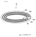
- Fig. 2 shows the above IC packaging film 22.
- the IC packaging film. 22 is fabricated in such a way that an antenna coil 22a which is formed in a spiral shape by etching Cu (copper) , for example, 9 ⁇ m thick is formed on one surface of a film 22b made of a PET (poly ethylene terephthalate) resin, for example, 38 ⁇ m thick, and that an electronic module 22e in which a bare chip IC 22d is packaged on a PET film.
- base material 22c for example, 25,. thick is mounted on the upper surface of the above antenna coil 22a.
- FIG. 3 shows the circuit arrangement (electronic circuit) of the above electronic module 22e.
- a control circuit 23 is one which is formed of, for example, a CPU, a ROM, a RAM etc. and which drives and controls individual circuit devices, a rectification circuit 23a rectifies the signal of an electromagnetic wave received by the antenna coil 22a, and a regulated voltage circuit 23b generates a DC supply voltage of regulated voltage on the basis of an electromotive force produced across the antenna coil 22a and feeds the supply voltage to individual circuits.
- a demodulation circuit 23c demodulates a signal from. the rectification circuit 23a, into digital data, a clock generation circuit 23d generates clock pulses for use in data processing, and a modulation circuit 23e modulates digital data to-be-transmitted, into a transmissible signal.
- An EEPROM 23f is a non-volatile storage medium, in which data are stored so as to be readable.
- the above control circuit 23 decodes the data demodulated by the demodulation circuit 23c.
- the control circuit 23 stores or reads out the data in or from the EEPROM 23f, and it performs the control of transmitting the data to-be-transmitted through the antenna 22a after the modulation thereof by the modulation circuit 23e.
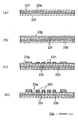
- Figs. 4(a) through 4(d) show the manufacturing steps of the antenna coil 22a included in the IC packaging film 22.
- both the surfaces of the PET film 22b being, for example, 25 ⁇ m thick are coated with layers of a urethane-based binder 22f, 22f by a roll coater method or the like so that each may be about 10 ⁇ m thick.
- the above binder layers 22f, 22f serve, not only for bonding a copper foil 22g, but also for bonding the high specific gravity resin material 21 as will be explained later.
- the copper foil 22g being, for example, 9 ⁇ m thick is put on one surface of the PET film 22b, and it is stacked and bonded there onto via a thermal lamination performed under the conditions of a temperature of 150°C and a pressure of 5kg/cm2.
- an etching resist pattern for the coil antenna 22a is printed and formed on the surface of the above stacked copper foil member. More specifically, an insulating etching resist ink 22h is printed on the copper foil 22g in a foil shape which has the number of turns, a line width, a pitch, and inside and outside diameters for attaining an L-value and a Q-value required as the characteristics of the antenna coil 22a, by employing, for example, gravure printing.
- etching resist ink 22h Used as the above etching resist ink 22h is an ink which is cured by heat or an active energy radiation.
- the active energy radiation may be ultraviolet radiation or electron rays.
- a photopolymerizer is mixed into the resist ink in use .
- the copper foil 22g is removed using Fecl 2 (120gr./lit.) as an etchant under the condition of a temperature of 50°C.
- the etching resist ink 22h is removed by a known process, whereby the film bearing the antenna coil can be obtained.
- the electron module 22e explained before is mounted on the film so as to form the IC packaging film 22.
- the etching resist ink 22h lying between electrical connection terminals is removed by mechanical friction based on the ultrasonic waves. Therefore, the IC packaging film 22 can be fabricated without the etching resist removal process.
- Figs. 5 (a) and 5 (b) show the manufacturing steps of the IC tag core 20 explained before.
- the high specific gravity resin material 21 is a material in which the powder of tungsten (W) or stainless steel (such as "SUS304") is dispersed and packed using, for example, a nylon 6 (polya8ide) resin as a binder.
- the molded compacts 21a, 21a are 8ade by subjecting the resin material 21 to injection molding which is performed under the conditions of, for example, a cylinder temperature of 270 - 280°C and a metal sold temperature of 80°C.
- the molded compacts 21a, 21a can be made by cutting them out of the high specific gravity resin material 21 which is formed in the shape of a bar. This method, however, is not suited for mass production.
- one molded compact 21a is formed with a recess 21b for accommodating the bare chip IC 22d of the electronic module 22e (refer to Fig. 2), at the same time as the molding thereof.
- the IC packaging film 22 is sandwiched in between the two molded compacts 21a, 21a as shown in Fig. 5(a), and it is sealed as shown in Fig. 5(b). Then, the IC tag core 20 is fabricated. More specifically, the IC packaging film 22 is arranged between the molded compacts 21a, 21a, and the resulting structure is loaded with a pressure of 20kg/cm2 for about 5 seconds in a state where it is held at a temperature of 120 - 200°C. Owing to this treatment, the urethane-based binder layers 22f, 22f at both the surfaces of the IC packaging film 22 are melted and are caused to flow under pressure. Besides, they are cured by subsequent cooling . Therefore, the three constituents of the upper and lower molded compacts 21a, 21a and the IC packaging film 22 are bonded, whereby the IC tag core 20 is fabricated.
- the working is carried out with the bare chip IC 22d of the electronic module 22e received in the recess 21b, so that the breakage of the bare chip IC 22d attributed to the pressure load can be avoided.
- Figs. 6(a) through 6(c) show a concept for the mass production of the IC tag cores 20.
- the IC packaging films 22 are fabricated in such a way that the antenna coils 22a and the electronic modules 22e are successively arrayed and mounted at predetermined intervals on the tape-shaped film 22b made of the PET resin.
- the antenna coils 22a can be formed by employing a method in which an etching mask is formed by gravure printing, followed by the etching of the copper foil 22g, and the electronic modules 22e are thereafter mounted.
- the copper foil 22g is left behind in the shape of stripes on both the sides of the tape 22b.
- the tension limit of the tape-shaped PET resin film 22b can be increased by the stripes of the copper foil 22g, and stable successive working can be realized.
- the molded compacts 21a, 21a formed of the high specific gravity resin material 21 beforehand are supplied from above and below the tape-shaped PET resin film 22b under positioned conditions, and the three constituents of the molded compacts 21a, 21a and the tape-shaped PET resin film 22b are joined.
- a treatment is performed by heating and pressing under the conditions explained with reference to Fig. 5(a), whereby the three constituents of the upper and lower molded compacts 21a, 21a and the IC packaging films 22 are bonded to fabricate the IC tag cores 20.
- IC packaging films 22 can be pulled out downwards without a post-working, for example, separation by a tool such as cutter .
- symbol 22i denotes a trace (or hole) formed after the pulling-out of the IC packaging film 22.
- Fig. 7 shows the schematic construction of an equipment for mass-producing the IC tag cores 20.
- the tape-shaped PET resin film. 22b is conveyed from a delivery drum 41 to a take-up drum 42 by roll feeders 43 ... intermittently at intervals permitting the molded compacts 21a, 21a to be joined, until it is taken up, and the molded compacts 21a, 21a are supplied during the conveyance of the tape 22b.
- Each pair of molded compacts 21a, 21a mentioned above are respectively held by holders 44, 45 disposed above and below, and are respectively supplied to the positions of the tape-shaped film. 22b corresponding to the IC packaging film 22.
- Each of the holders 44,45 includes heating means (not shown).
- the upper holder 44 performs vertical movements by a suitable cylinder mechanism (not shown) and presses the tape-shaped film 22b under a predetermined pressure.
- the mass production of the IC tag cores 20 as shown in Figs. 6 (a) through 6 (c) can be realized by such an aspect of the equipment .
- Figs. 8(a) through 8(c) show working steps for manufacturing the coin-shaped IC tag 10 in such a way that the whole surface of the IC tag core 20 produced by the above process is covered with the colorable covering resin 30.
- the molded compacts 21a, 21a for forming the IC tag core 20 is made of the high specific gravity resin material 21 in which the metal powder of tungsten (W) or stainless steel (such as "SUS304") is dispersed and mixed. Accordingly, even when the binder resin of the resin material 21 is colored, a desired tint is difficult to be obtained. Therefore, the covering resin 30 is formed by covering the surface of the IC tag core 20 with a colorable resin in accordance with a method explained below.
- a hard material for example, an urethane-acrylate-based UV curable resin
- nylon polyamide resin
- the whole surface of the IC tag core 20 formed of the resin 21 is processed by the plasma.. of oxygen, nitrogen, an inert gas or the like so as to be endowed with a critical surface tension of at least 55dynes/cm.
- the surface of the IC tag core 20 is coated with the hard coat material 30a by spraying, dipping, a roll coater method or the like.
- the hard coat material 30a is dried at 60°C for about 1 - 3 minutes so as to sufficiently volatilize its solvent . Then, subsequent cracking can be suppressed, and the coating of high hardness can be obtained.
- the above applied hard coat material 30a is irradiated with UV radiation so as to perfectly cure a coating film.
- the UV irradiation on this occasion is carried out by, for example, a high-pressure mercury vapor lamp of 80W/cm located at a distance of 15 - 20cm, for 2 seconds.
- the covering resin 30 can be obtained.
- the coin-shaped IC tag 10 is finished up. Since, in this case, the covering resin 30 is colorable, the appearance of design of the coin-shaped IC tag 10 can be enhanced by selecting a tint.
- the thickness of the layer of the covering resin 30 is about 0. 2mm. Therefore, in the case where the geometries of the coin are limited to the diameter of 30mm ⁇ and the thickness of 2- as explained before, the high specific gravity resin material 21 can be used in a sufficient amount. It is accordingly possible to obtain the coin-shaped IC tag 10 affording a satisfactory feeling of weightiness.
- the PET resin film 22b can be replaced with the film material of a polyimide resin (PI), a polyphenylene sulfite resin (PPS), polyethylene naphthalate (PEN) or the like.
- the copper foil 22g can be replaced with an aluminium foil.
- the resin binder of the high specific gravity resin material 21 for .mixing the metal powder it is possible to use any of various resins such as a polyphenylene sulfite resin (PPS), a polycarbonate resin (PC), an acrylonitrile-butadiene styrene resin (ABS), a polymethyl methacrylate resin (PMMA), a polybutylene terephthalate resin (PBT), and "Nolyl” or a polyphenylene oxide resin (PPO) .
- PPS polyphenylene sulfite resin
- PC polycarbonate resin
- ABS acrylonitrile-butadiene styrene resin
- PMMA polymethyl methacrylate resin
- PBT polybutylene terephthalate resin
- PPO polyphenylene oxide resin
- the urethane-based binder 22f at both the surfaces of the IC packaging film 22 is used for bonding the three constituents of this IC packaging fil8 22 and the two molded compacts 21a, 21a formed of the high specific gravity resin material 21.
- the three constituents can be joined by utilizing a bonding power which is possessed by the binder resin itself for forming the two molded compacts 21a, 21a.
- Figs. 9(a) and 9(b) show the above example in which the three constituents are joined by utilizing the bonding power of the binder resin itself.
- the PPS is employed as the binder resin constituting the high specific gravity resin material 21
- the PET resin is employed for the film 22b of the IC packaging film 22.
- the IC packaging film 22 one surface of which has had the urethane-based binder 22f removed there from is interposed between the two molded compacts 21a, 21a made of the high specific gravity resin material 21.
- the resulting structure is heated to a temperature of at least 240°C, it is loaded with a pressure of 20kg/cm2 for about 2 seconds.
- the PET being the film material is melted and is partially removed from the interfaces between the IC packaging film 22 and the molded compacts 21a, 21a.
- the IC tag core 20 can be manufactured.
- the binder resin components of the molded compacts 21a, 21a are fused and bonded by the heating in the above example, the fusion bonding may well be performed by projecting ultrasonic waves of, for example, 40kHz.
- the covering resin 30 can be thickened by forming the resin layer 30 in accordance with injection molding.
- protrusions 20b ... each of which is set at a height corresponding to the thickness of the layer of the covering resin 30 are formed on the upper and lower surfaces of the IC tag core 20.
- the protrusions 20b ... may be simultaneously formed at the formation of the molded compacts 21a, 21a of the high specific gravity resin material 21.
- the IC tag core 20 with the protrusions 20b ... prepared as explained above is set in the cavity 51 of a metal mold 50, and the starting resin of the covering resin 30 is poured into the metal mold 50.
- the protrusions 20b ... serve as the supporter of the IC tag core 20, and hence, the injection molding can be performed.
- each protrusion 20b becomes the thickness of the layer of the covering resin 30, and a sufficient thickness can be attained.
- the bonding strength between the IC tag core 20 and the covering resin 30 is heightened.
- Figs. 11(a) and 11(b) show another example of the manufacture of the coin-shaped IC tag 10.
- the .molded compacts 21a, 21a are formed of the high specific gravity resin material 21 by injection molding, each molded compact 21a and the covering resin 30 are simultaneously formed by dichroic molding, thereby to make the molded compact 21a with the covering resin 30.
- the IC packaging film 22 is sandwiched in between the pair of molded compacts 21a, 21a with the covering resin 30 prepared as explained above. Subsequently, as shown in Fig. 11(b), the three constituents are bonded .
- the bonding here can be done by any of the layers of the binder 22f applied at both the surfaces of the IC packaging film. 22, fusion bonding, and ultrasonic waves.
- the coin-shaped IC tag 10 can be manufactured in this way.
- Fig. 12 shows another example of the coin-shaped IC tag 10.
- the IC packaging film 22 is joined onto either surface of one molded compact 21a formed of the high specific gravity resin material 21, and the whole surface of the resulting structure is covered with the covering resin 30.
- the circumferential part of this tag 10 is thickened in the radial direction thereof.
- Fig. 13 shows still another example of the coin-shaped IC tag 10.
- the outer peripheral edge of the IC tag core 20 is covered with the covering resin 30.
- Fig. 14 shows yet another example of the coin-shaped IC tag 10.
- one surface and the outer peripheral edge of the IC tag core 20 are covered with the covering resin 30.
- the coin-shaped IC tag 10 can be endowed with a predetermined weight, it ensures a normal operation without an inferior operation ascribable to an insufficient weight, even in its use as a substitute for cash . Moreover, since the coin-shaped IC tag 10 can afford a satisfactory feeling of weightiness as a value medium, it does not degrade the feeling of valuableness as the substitute for cash. Accordingly, the coin-shaped IC tag 10 can attain the satisfactory functions as the substitute for cash.
- the "IC packaging base member” of this invention corresponds to the IC packaging film 22 of the embodiments.
- the “base material” corresponds to the PET film 22b.
- the “electronic circuit” corresponds to the antenna coil 22a and the electronic module 22e.
- this invention is not restricted only to the construction disclosed in the aspect of performance, but it can take different aspects of performance along the technical idea thereof.
Landscapes
- Engineering & Computer Science (AREA)
- Physics & Mathematics (AREA)
- General Physics & Mathematics (AREA)
- Theoretical Computer Science (AREA)
- Computer Hardware Design (AREA)
- Microelectronics & Electronic Packaging (AREA)
- Credit Cards Or The Like (AREA)
- Control Of Vending Devices And Auxiliary Devices For Vending Devices (AREA)
Applications Claiming Priority (2)
| Application Number | Priority Date | Filing Date | Title |
|---|---|---|---|
| JP2000186423A JP3534042B2 (ja) | 2000-06-21 | 2000-06-21 | コイン形icタグおよびその製造方法 |
| JP2000186423 | 2000-06-21 |
Publications (2)
| Publication Number | Publication Date |
|---|---|
| EP1168236A2 true EP1168236A2 (fr) | 2002-01-02 |
| EP1168236A3 EP1168236A3 (fr) | 2002-07-24 |
Family
ID=18686587
Family Applications (1)
| Application Number | Title | Priority Date | Filing Date |
|---|---|---|---|
| EP01304997A Withdrawn EP1168236A3 (fr) | 2000-06-21 | 2001-06-08 | Transpondeur en forme de pièce de monnaie et son procédé de fabrication |
Country Status (4)
| Country | Link |
|---|---|
| US (2) | US6621153B2 (fr) |
| EP (1) | EP1168236A3 (fr) |
| JP (1) | JP3534042B2 (fr) |
| AU (1) | AU782215B2 (fr) |
Cited By (3)
| Publication number | Priority date | Publication date | Assignee | Title |
|---|---|---|---|---|
| WO2003069012A1 (fr) * | 2002-02-14 | 2003-08-21 | National Institute Of Water & Atmospheric Research Limited | Procede de fabrication d'etiquette et appareil |
| US8202238B2 (en) | 2003-12-15 | 2012-06-19 | Semiconductor Energy Laboratory Co., Ltd. | Method for manufacturing thin film integrated circuit device, noncontact thin film integrated circuit device and method for manufacturing the same, and idtag and coin including the noncontact thin film integrated circuit device |
| US8360327B2 (en) | 2002-02-14 | 2013-01-29 | Ensid Investments Ltd. | Animal transponder tag |
Families Citing this family (48)
| Publication number | Priority date | Publication date | Assignee | Title |
|---|---|---|---|---|
| JP4564136B2 (ja) * | 2000-06-23 | 2010-10-20 | マクセル精器株式会社 | 非接触式のicカード |
| JP4620303B2 (ja) * | 2001-09-20 | 2011-01-26 | 株式会社東海理化電機製作所 | 半導体装置及びその製造方法 |
| JP4143340B2 (ja) * | 2002-06-17 | 2008-09-03 | 日立マクセル株式会社 | 非接触通信式情報担体 |
| CN1697187B (zh) | 2003-12-19 | 2011-05-04 | 株式会社半导体能源研究所 | 半导体集成电路、半导体器件和半导体集成电路的制造方法 |
| JP4554195B2 (ja) * | 2003-12-24 | 2010-09-29 | 本田技研工業株式会社 | 車両管理システム |
| US7566010B2 (en) * | 2003-12-26 | 2009-07-28 | Semiconductor Energy Laboratory Co., Ltd. | Securities, chip mounting product, and manufacturing method thereof |
| US7632721B2 (en) * | 2004-02-06 | 2009-12-15 | Semiconductor Energy Laboratory Co., Ltd. | Method for manufacturing thin film integrated circuit, and element substrate |
| US7820529B2 (en) | 2004-03-22 | 2010-10-26 | Semiconductor Energy Laboratory Co., Ltd. | Method for manufacturing integrated circuit |
| JP4491539B2 (ja) | 2004-06-11 | 2010-06-30 | オムロン株式会社 | コイン型記録媒体、記録媒体処理装置 |
| US7927971B2 (en) | 2004-07-30 | 2011-04-19 | Semiconductor Energy Laboratory Co., Ltd. | Method for manufacturing semiconductor device |
| ES2617675T3 (es) * | 2004-10-28 | 2017-06-19 | Assa Abloy Ab | Dispositivo de sellado de seguridad que comprende una etiqueta RFID |
| CN101073297A (zh) * | 2004-12-03 | 2007-11-14 | 哈里斯股份有限公司 | 电子部件的制造方法及电子部件的制造装置 |
| DE602005024861D1 (de) * | 2004-12-03 | 2010-12-30 | Hallys Corp | Zwischenglied-bondierungseinrichtung |
| JP4709989B2 (ja) * | 2004-12-28 | 2011-06-29 | 旭精工株式会社 | Icトークン、icトークンの射出成型型装置及びicトークンの製造方法 |
| US20080138889A1 (en) * | 2005-02-10 | 2008-06-12 | Semiconductor Energy Laboratory Co., Ltd. | Semiconductor Device |
| JP4810531B2 (ja) | 2005-04-06 | 2011-11-09 | 株式会社 ハリーズ | 電子部品の製造装置 |
| JP4880291B2 (ja) * | 2005-11-24 | 2012-02-22 | トッパン・フォームズ株式会社 | アンテナシート |
| US20080074271A1 (en) * | 2006-09-27 | 2008-03-27 | Science Applications International Corporation | Radio frequency transponders having three-dimensional antennas |
| US20100144449A1 (en) * | 2006-11-13 | 2010-06-10 | Elixir Gaming Technologies Inc. | Gaming token |
| JP2008246103A (ja) * | 2007-03-30 | 2008-10-16 | Angel Shoji Kk | Rfidを内包した遊戯用代用貨幣およびその製造方法 |
| JP2008250847A (ja) * | 2007-03-30 | 2008-10-16 | Angel Shoji Kk | Rfidを内蔵した遊戯用代用貨幣およびその製造方法 |
| JP2009170476A (ja) * | 2008-01-11 | 2009-07-30 | Panasonic Corp | 半導体装置および半導体装置の製造方法 |
| JP5586920B2 (ja) * | 2008-11-20 | 2014-09-10 | 株式会社半導体エネルギー研究所 | フレキシブル半導体装置の作製方法 |
| JP5427401B2 (ja) * | 2008-12-19 | 2014-02-26 | 株式会社ユニバーサルエンターテインメント | Idタグ内蔵型遊技媒体 |
| DE102009015579A1 (de) * | 2009-03-30 | 2010-10-07 | Soheil Hamedani | Münze mit integrierter RFID-Identifiziervorrichtung und Verfahren zu dessen Herstellung |
| JP5482300B2 (ja) * | 2010-03-03 | 2014-05-07 | Nok株式会社 | Icタグの製造方法 |
| SG11201402561PA (en) * | 2011-12-28 | 2014-08-28 | Nhk Spring Co Ltd | Contactless information medium, contactless information medium bobbin member, main body member for contactless information medium, manufacturing method for contactless information medium |
| WO2013172847A1 (fr) * | 2012-05-17 | 2013-11-21 | Intel Corporation | Moulage d'insert de film pour la fabrication de dispositifs |
| US9147149B2 (en) * | 2013-06-13 | 2015-09-29 | L'oreal | RFID tag for a personal care appliance |
| US11074780B2 (en) | 2015-08-03 | 2021-07-27 | Angel Playing Cards Co., Ltd. | Management system of substitute currency for gaming |
| US10970962B2 (en) | 2015-08-03 | 2021-04-06 | Angel Playing Cards Co., Ltd. | Management system of substitute currency for gaming |
| EP4234053B1 (fr) | 2015-08-03 | 2025-05-21 | Angel Playing Cards Co., Ltd. | Système de gestion de devise de substitution pour jeux |
| ES2985532T3 (es) | 2015-08-03 | 2024-11-06 | Angel Playing Cards Co Ltd | Sistema de detección de fraude en sala de juegos |
| AU2016356233A1 (en) | 2015-11-19 | 2018-06-07 | Angel Group Co., Ltd. | Table game management system, substitute currency for gaming, and inspection device |
| DE102015120396B8 (de) * | 2015-11-25 | 2025-04-10 | Infineon Technologies Austria Ag | Halbleiterchip-Package umfassend Seitenwandkennzeichnung |
| JP2017202169A (ja) * | 2016-05-12 | 2017-11-16 | 旭化工株式会社 | カジノ用プラーク |
| US11671807B2 (en) * | 2016-11-11 | 2023-06-06 | Carnival Corporation | Wireless device and methods for making and using the same |
| US10499228B2 (en) | 2016-11-11 | 2019-12-03 | Carnival Corporation | Wireless guest engagement system |
| US10045184B2 (en) | 2016-11-11 | 2018-08-07 | Carnival Corporation | Wireless guest engagement system |
| US10817768B1 (en) | 2019-12-20 | 2020-10-27 | Capital One Services, Llc | Systems and methods for preventing chip fraud by inserts in chip pocket |
| US10888940B1 (en) | 2019-12-20 | 2021-01-12 | Capital One Services, Llc | Systems and methods for saw tooth milling to prevent chip fraud |
| US10810475B1 (en) | 2019-12-20 | 2020-10-20 | Capital One Services, Llc | Systems and methods for overmolding a card to prevent chip fraud |
| US10977539B1 (en) | 2019-12-20 | 2021-04-13 | Capital One Services, Llc | Systems and methods for use of capacitive member to prevent chip fraud |
| US11049822B1 (en) | 2019-12-20 | 2021-06-29 | Capital One Services, Llc | Systems and methods for the use of fraud prevention fluid to prevent chip fraud |
| JP7198862B2 (ja) | 2020-04-20 | 2023-01-04 | エンゼルグループ株式会社 | 遊技用代用貨幣及びその製造方法 |
| US11715103B2 (en) | 2020-08-12 | 2023-08-01 | Capital One Services, Llc | Systems and methods for chip-based identity verification and transaction authentication |
| KR20230109563A (ko) * | 2022-01-13 | 2023-07-20 | 엔제루 구루푸 가부시키가이샤 | 관리 시스템 및 게임용 화폐 |
| JP7732929B2 (ja) * | 2022-03-16 | 2025-09-02 | 日本発條株式会社 | 非接触情報媒体 |
Family Cites Families (10)
| Publication number | Priority date | Publication date | Assignee | Title |
|---|---|---|---|---|
| JPH03500033A (ja) * | 1988-06-21 | 1991-01-10 | ダブリュー アンド ティー エイヴァリー リミテッド | ポータブル電子トークンの製造法 |
| JPH02101599A (ja) | 1988-10-11 | 1990-04-13 | Matsushita Electric Ind Co Ltd | コイン状の情報媒体 |
| FR2723228B1 (fr) * | 1994-07-26 | 1996-09-20 | Bourgogne Grasset | Jeton de jeu perfectionne |
| US5906863A (en) * | 1994-08-08 | 1999-05-25 | Lombardi; John | Methods for the preparation of reinforced three-dimensional bodies |
| DE69812919T2 (de) * | 1997-03-10 | 2003-11-13 | Etablissements Bourgogne Et Grasset, Savigny Les Beaune | Marke mit elektronischen chip |
| FR2760330B1 (fr) * | 1997-03-10 | 1999-05-07 | Bourgogne Grasset | Jeton composite |
| FR2760331B1 (fr) * | 1997-03-10 | 1999-04-30 | Bourgogne Grasset | Jeton a puce electronique |
| JPH111083A (ja) * | 1997-06-13 | 1999-01-06 | Dainippon Printing Co Ltd | 非接触icカード及びその製造方法 |
| JP3491670B2 (ja) | 1998-04-08 | 2004-01-26 | 三菱マテリアル株式会社 | 盗難防止用タグ及びその製造方法 |
| EP0964361A1 (fr) * | 1998-06-08 | 1999-12-15 | International Business Machines Corporation | Protection d'information sensible contenue dans les cartes à puce |
-
2000
- 2000-06-21 JP JP2000186423A patent/JP3534042B2/ja not_active Expired - Lifetime
-
2001
- 2001-06-08 EP EP01304997A patent/EP1168236A3/fr not_active Withdrawn
- 2001-06-20 AU AU53935/01A patent/AU782215B2/en not_active Ceased
- 2001-06-20 US US09/884,464 patent/US6621153B2/en not_active Expired - Lifetime
-
2003
- 2003-08-08 US US10/636,583 patent/US6873033B2/en not_active Expired - Lifetime
Non-Patent Citations (1)
| Title |
|---|
| None * |
Cited By (4)
| Publication number | Priority date | Publication date | Assignee | Title |
|---|---|---|---|---|
| WO2003069012A1 (fr) * | 2002-02-14 | 2003-08-21 | National Institute Of Water & Atmospheric Research Limited | Procede de fabrication d'etiquette et appareil |
| AU2003206473B2 (en) * | 2002-02-14 | 2008-08-28 | Ensid Investments Ltd | Method and apparatus for the manufacture of a tag |
| US8360327B2 (en) | 2002-02-14 | 2013-01-29 | Ensid Investments Ltd. | Animal transponder tag |
| US8202238B2 (en) | 2003-12-15 | 2012-06-19 | Semiconductor Energy Laboratory Co., Ltd. | Method for manufacturing thin film integrated circuit device, noncontact thin film integrated circuit device and method for manufacturing the same, and idtag and coin including the noncontact thin film integrated circuit device |
Also Published As
| Publication number | Publication date |
|---|---|
| AU782215B2 (en) | 2005-07-14 |
| JP3534042B2 (ja) | 2004-06-07 |
| US6621153B2 (en) | 2003-09-16 |
| EP1168236A3 (fr) | 2002-07-24 |
| US6873033B2 (en) | 2005-03-29 |
| AU5393501A (en) | 2002-01-03 |
| US20040026520A1 (en) | 2004-02-12 |
| JP2002007989A (ja) | 2002-01-11 |
| US20020024439A1 (en) | 2002-02-28 |
Similar Documents
| Publication | Publication Date | Title |
|---|---|---|
| EP1168236A2 (fr) | Transpondeur en forme de pièce de monnaie et son procédé de fabrication | |
| JP2002007989A5 (fr) | ||
| CN109273210B (zh) | 线圈装置 | |
| CN100403462C (zh) | 薄型变压器及其制造方法 | |
| JP6462780B2 (ja) | 無線電力受信装置及びその製造方法 | |
| US5880934A (en) | Data carrier having separately provided integrated circuit and induction coil | |
| US7345645B2 (en) | Method of manufacturing substrate for circuit board and smart label having the substrate | |
| WO1999004365A1 (fr) | Module a circuit integre, procede de fabrication dudit module et carte a circuit integre dotee dudit module | |
| JP2003524811A (ja) | 埋込み電子装置を有する製品とその製作方法 | |
| TW201218087A (en) | Radio frequency identification device in polycarbonate and its manufacturing method | |
| WO2010013992A1 (fr) | Bobine hélicoïdale en ruban mince flexible | |
| US20020125546A1 (en) | Semiconductor device, production method therefor, and electrophotographic apparatus | |
| EP1132861A2 (fr) | Etiquette à circuit intégré et méthode de production | |
| JP2004021649A (ja) | 非接触通信式情報担体 | |
| JP5262803B2 (ja) | Icタグ及びicタグの製造方法 | |
| KR101204074B1 (ko) | 스마트 라벨 및, 그것의 제조 방법 | |
| JP2004021648A (ja) | 非接触通信式情報担体 | |
| JP2004021650A (ja) | 非接触通信式情報担体 | |
| KR100627045B1 (ko) | 집적회로카드용 반도체패키지와 이의 제조방법 | |
| JP2006260670A (ja) | 光ディスクの製造方法および光ディスク | |
| KR20260044255A (ko) | 스마트 카드에 통합하기 위한 인쇄 회로, 이러한 인쇄 회로를 갖는 스마트 카드, 및 스마트 카드의 제조 공정에 사용하기 위한 릴-투-릴 테이프 | |
| JPH06290958A (ja) | ロータリートランス |
Legal Events
| Date | Code | Title | Description |
|---|---|---|---|
| PUAI | Public reference made under article 153(3) epc to a published international application that has entered the european phase |
Free format text: ORIGINAL CODE: 0009012 |
|
| AK | Designated contracting states |
Kind code of ref document: A2 Designated state(s): AT BE CH CY DE DK ES FI FR GB GR IE IT LI LU MC NL PT SE TR |
|
| AX | Request for extension of the european patent |
Free format text: AL;LT;LV;MK;RO;SI |
|
| PUAL | Search report despatched |
Free format text: ORIGINAL CODE: 0009013 |
|
| AK | Designated contracting states |
Kind code of ref document: A3 Designated state(s): AT BE CH CY DE DK ES FI FR GB GR IE IT LI LU MC NL PT SE TR |
|
| AX | Request for extension of the european patent |
Free format text: AL;LT;LV;MK;RO;SI |
|
| 17P | Request for examination filed |
Effective date: 20021011 |
|
| AKX | Designation fees paid |
Designated state(s): AT BE CH CY DE DK ES FI FR GB GR IE IT LI LU MC NL PT SE TR |
|
| 17Q | First examination report despatched |
Effective date: 20061206 |
|
| STAA | Information on the status of an ep patent application or granted ep patent |
Free format text: STATUS: THE APPLICATION IS DEEMED TO BE WITHDRAWN |
|
| 18D | Application deemed to be withdrawn |
Effective date: 20070417 |