EP1168452A2 - Halbleiterbauelement mit vertikalem Bipolartransistor - Google Patents
Halbleiterbauelement mit vertikalem Bipolartransistor Download PDFInfo
- Publication number
- EP1168452A2 EP1168452A2 EP01114890A EP01114890A EP1168452A2 EP 1168452 A2 EP1168452 A2 EP 1168452A2 EP 01114890 A EP01114890 A EP 01114890A EP 01114890 A EP01114890 A EP 01114890A EP 1168452 A2 EP1168452 A2 EP 1168452A2
- Authority
- EP
- European Patent Office
- Prior art keywords
- region
- semiconductor region
- semiconductor
- collector
- impurity
- Prior art date
- Legal status (The legal status is an assumption and is not a legal conclusion. Google has not performed a legal analysis and makes no representation as to the accuracy of the status listed.)
- Withdrawn
Links
- 239000004065 semiconductor Substances 0.000 title claims abstract description 172
- 239000012535 impurity Substances 0.000 claims abstract description 36
- 238000012886 linear function Methods 0.000 claims 1
- 230000003071 parasitic effect Effects 0.000 description 32
- 230000010355 oscillation Effects 0.000 description 19
- XUIMIQQOPSSXEZ-UHFFFAOYSA-N Silicon Chemical compound [Si] XUIMIQQOPSSXEZ-UHFFFAOYSA-N 0.000 description 9
- 229910052710 silicon Inorganic materials 0.000 description 9
- 239000010703 silicon Substances 0.000 description 9
- 239000003990 capacitor Substances 0.000 description 7
- 238000009792 diffusion process Methods 0.000 description 7
- 230000005540 biological transmission Effects 0.000 description 5
- 238000010586 diagram Methods 0.000 description 5
- 238000004891 communication Methods 0.000 description 4
- 230000007423 decrease Effects 0.000 description 4
- 239000000758 substrate Substances 0.000 description 4
- 230000003247 decreasing effect Effects 0.000 description 3
- 238000000034 method Methods 0.000 description 2
- 230000006835 compression Effects 0.000 description 1
- 238000007906 compression Methods 0.000 description 1
- 238000005468 ion implantation Methods 0.000 description 1
- 238000012986 modification Methods 0.000 description 1
- 230000004048 modification Effects 0.000 description 1
Images


Classifications
-
- H—ELECTRICITY
- H10—SEMICONDUCTOR DEVICES; ELECTRIC SOLID-STATE DEVICES NOT OTHERWISE PROVIDED FOR
- H10D—INORGANIC ELECTRIC SEMICONDUCTOR DEVICES
- H10D84/00—Integrated devices formed in or on semiconductor substrates that comprise only semiconducting layers, e.g. on Si wafers or on GaAs-on-Si wafers
-
- H—ELECTRICITY
- H10—SEMICONDUCTOR DEVICES; ELECTRIC SOLID-STATE DEVICES NOT OTHERWISE PROVIDED FOR
- H10D—INORGANIC ELECTRIC SEMICONDUCTOR DEVICES
- H10D10/00—Bipolar junction transistors [BJT]
- H10D10/40—Vertical BJTs
- H10D10/421—Vertical BJTs having both emitter-base and base-collector junctions ending at the same surface of the body
-
- H—ELECTRICITY
- H10—SEMICONDUCTOR DEVICES; ELECTRIC SOLID-STATE DEVICES NOT OTHERWISE PROVIDED FOR
- H10D—INORGANIC ELECTRIC SEMICONDUCTOR DEVICES
- H10D62/00—Semiconductor bodies, or regions thereof, of devices having potential barriers
- H10D62/10—Shapes, relative sizes or dispositions of the regions of the semiconductor bodies; Shapes of the semiconductor bodies
- H10D62/13—Semiconductor regions connected to electrodes carrying current to be rectified, amplified or switched, e.g. source or drain regions
- H10D62/137—Collector regions of BJTs
Definitions
- the present invention relates to a semiconductor device and more particularly to the structure of a collector region of a vertical bipolar transistor.
- FIG. 1 is a cross-sectional view of a pnp bipolar transistor.
- a p + -type buried layer 110 which serves as a collector region, is formed in an n-type silicon substrate 100.
- a p - -type epitaxial silicon layer 120 is formed on the surface of the substrate 100.
- the layer 120 serves as a collector region whose concentration is lower than that of the p + -type buried layer 110.
- An n-type diffusion layer 130 which serves as a base region, is formed in a surface area of the layer 120.
- a p + -type diffusion layer 140 which serves as an emitter region, is formed in a surface area of the layer 130.
- two p + -type diffusion layers 150 which contact the p + -type buried layer 110, are formed in the p - -type epitaxial silicon layer 120.
- the bipolar transistor is thus obtained as described above.
- the collector region has a two-layer structure of the layer 110 doped with impurities to make the concentration relatively high and the layer 120 doped with impurities to make the concentration lower than that of the layer 110.
- the bipolar transistor When the bipolar transistor performs a normal operation, a reversed bias is applied to a pn junction between the base and collector regions.
- the impurity concentration of the collector region 120 is lower than that of the base region 130, so that most part of a depletion layer 160 formed at the pn junction is included in the collector region 120.
- the base-to-collector parasitic capacitance almost depends upon the depletion layer formed in the collector region 120.
- the width (thickness) Dc of the collector region 120 is set greater than that Wc of the depletion layer formed in the collector region 120 by an applied voltage in the normal operation.
- the base-to-collector parasitic capacitance in the prior art bipolar transistor depends upon the depletion layer formed in the collector region 120 doped with impurities to make the concentration of the collector region relatively low.
- the depletion layer is formed widely and thus the parasitic capacitance is limited to a relatively small value.
- the width of the depletion layer is greatly varied with a voltage applied between the base and collector, as is the parasitic capacitance.
- the base-to-collector parasitic capacitance is greatly changed with the applied voltage, and thus the oscillation frequency of the oscillation circuit is widely varied (pushing).
- the collector region of the prior art vertical bipolar transistor has the two-layer structure described above.
- the structure includes the collector region 110 doped with impurities to make the concentration of the region 110 high and the collector region 120 doped with impurities to make the concentration of the region 120 low and connected to the base region.
- the low-impurity-concentration collector region 120 is formed more widely than the depletion layer generated by the voltage applied in the normal operation and most of the region 120 is formed in the collector region due to a difference in impurity concentration.
- the base-to-collector parasitic capacitance therefore depends upon the depletion layer formed in the low-impurity-concentration collector region 120, and the depletion layer is formed widely. The parasitic capacitance is limited to a relatively small value.
- the width of the depletion layer is widely varied with the voltage applied between the base and collector and thus the parasitic capacitance varies greatly.
- the base-to-collector parasitic capacitance is greatly changed with the applied voltage and thus the parasitic capacitance is greatly varied, with the result that the oscillation frequency of the oscillation circuit is widely varied.
- the present invention has been developed in consideration of the above situation and an object thereof is to provide a semiconductor device capable of suppressing variations of the width of a depletion layer due to an applied voltage while reducing the parasitic capacitance at a pn junction.
- a semiconductor device comprises a first semiconductor region of a first conductivity type, the first semiconductor region serving as a collector region; a second semiconductor region of the first conductivity type, the second semiconductor region being provided on the first semiconductor region and serving as a collector region whose impurity concentration is lower than that of the first semiconductor region; a third semiconductor region of a second conductivity type, the third semiconductor region being provided in the second semiconductor region and serving as a base region; and a fourth semiconductor region of the first conductivity type, the fourth semiconductor region being provided in the third semiconductor region and serving as an emitter region, wherein the second semiconductor region is thinner than a depletion layer formed in the collector region when a potential difference between the base region and the emitter region is substantially equal to a potential difference between the collector region and the emitter region.
- a base-to-emitter voltage Vbe is almost equal to a collector-to-emitter voltage Vce in a bipolar transistor including a high-impurity-concentration region and a low-impurity-concentration region contacting the base region.
- the low-impurity-concentration region is set thinner than a depletion layer formed in the collector region when the base-to-collector voltage Vbc is almost 0V.
- the variation of the depletion layer when a reversed bias is applied between the base and collector can be reduced and so can be that of parasitic capacitance generated between the base and collector in the normal operation, keeping the parasitic capacitance at the same level as that of the prior art. If an oscillation circuit is constituted of the bipolar transistor, the variation of oscillation frequency of the oscillation circuit can be suppressed and the operation reliability of the oscillation circuit can be improved.
- a semiconductor device comprises a first semiconductor region of a first conductivity type, the first semiconductor region serving as a collector region; a second semiconductor region of the first conductivity type, the second semiconductor region being provided on the first semiconductor region and serving as a collector region whose impurity concentration is lower than that of the first semiconductor region; a third semiconductor region of a second conductivity type, the third semiconductor region being provided in the second semiconductor region and serving as a base region; and a fourth semiconductor region of the first conductivity type, the fourth semiconductor region being provided in the third semiconductor region and serving as an emitter region, wherein the first and second semiconductor regions have an impurity-concentration profile set such that a depletion layer formed in the collector region reaches the semiconductor region when a potential difference between the base region and the emitter region is substantially equal to a potential difference between the collector region and the emitter region.
- an impurity-concentration profile is set such that a depletion layer formed in the collector region reaches the high-impurity-concentration region when a base-to-emitter voltage Vbe is almost equal to a collector-to-emitter voltage Vce or a base-to-collector voltage Vbc is almost 0V.
- a semiconductor device comprises a first semiconductor region of a first conductivity type, the first semiconductor region serving as a collector region; a second semiconductor region of the first conductivity type, the second semiconductor region being provided on the first semiconductor region and serving as a collector region whose impurity concentration is lower than that of the first semiconductor region; a third semiconductor region of a second conductivity type, the third semiconductor region being provided in the second semiconductor region and serving as a base region; and a fourth semiconductor region of the first conductivity type, the fourth semiconductor region being provided in the third semiconductor region and serving as an emitter region, wherein the second semiconductor region is thinner than a depletion layer formed in the collector region when a potential difference between the base region and the emitter region is substantially equal to a potential difference between the collector region and the emitter region, and the second semiconductor region has an impurity-concentration profile set such that impurity concentration increases in a depth direction.
- an impurity-concentration profile is set such that the impurity concentration of the low-impurity-concentration collector of the bipolar transistor increases in the depth direction.
- FIG. 2 is a cross-sectional view of a pnp bipolar transistor of the first embodiment.
- a p - -type epitaxial silicon layer 12 is formed on the surface of the substrate 10.
- the layer 12 serves as a collector region whose concentration is lower than that of the p + -type buried layer 11.
- two p + -type diffusion layers 15, which contact the p + -type buried layer 11, are formed in the p - -type epitaxial silicon layer 12. The bipolar transistor is thus obtained as described above.
- the thickness Dc of the p - -type epitaxial silicon layer 12 is set smaller than the width (thickness) Wc of a depletion layer formed in the layer 12 by a pn junction between the p - -type epitaxial silicon layer 12 and n-type diffusion layer 13 in the normal operation.
- Cbc Cbc0/(1 - Vd/ ⁇ 0) 1/2
- Vd is a base-to-collector voltage
- Cbc0 is parasitic capacitance obtained when the voltage Vd is equal to 0V
- ⁇ 0 is a built-in potential
- the impurity concentration of the collector region 12 is lower than that of the base region 13. Most part of a depletion layer 16 at the pn junction is therefore formed widely in the collector region 12. Thus, the base-to-collector parasitic capacitance almost depends upon the depletion layer formed in the collector region 12.
- the parasitic capacitance can be considered to be a capacitor using both ends of the depletion layer formed between the base and collector regions as parallel flat electrodes. If a voltage applied between the base and collector regions increases, the depletion layer expands and the capacitance decreases. Under this concept, let us consider a method for determining the parasitic capacitance by calculation.
- the width of the depletion layer is proportional to the applied voltage (reversed bias) and inversely proportional to the impurity concentration. If, therefore, the impurity concentration of the collector region is set high, the variations of the depletion layer due to the applied voltage decreases, but the width d(Vd) of the depletion layer becomes small; accordingly, the capacitance increases and varies greatly.
- the concentration of the collector region is set in such a manner that the depletion layer is formed to span both the lower- and higher-concentration layers of the collector region.
- the variations of the depletion layer can thus be limited to the same level as that when the collector region is formed of only the high-concentration layer, while the parasitic capacitance is limited to substantially the same level as that when the collector region is formed of only the low-concentration layer.
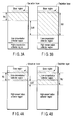
- FIGS. 3A and 3B illustrate a depletion layer formed between the base and collector of the prior art bipolar transistor.
- the transistor performs a normal operation and, in other words, a pn junction between the base and collector turns off.
- a reversed bias is applied to the pn junction.
- FIGS. 4A and 4B illustrate a depletion layer formed between the base and collector of the bipolar transistor according to the present invention.
- the transistor performs a normal operation and, in other words, a pn junction between the base and collector turns off.
- a reversed bias is applied to the pn junction.
- the width of a depletion layer formed in the collector region when a bias necessary for the normal operation is applied between the collector and emitter regions is indicated by Wc. It is needless to say that the depletion layer is all formed in a low-impurity-concentration region of the collector region.
- the width of a depletion layer formed in the collector region is almost equal to the width Wc of the depletion layer of the prior art bipolar transistor.
- the depletion layer is formed in a low-impurity-concentration region of the collector region but part of the depletion layer is included in a high-impurity-concentration region thereof.
- the end portions of the depletion layer are formed in the high-impurity-concentration region. Since, however, most of the depletion layer is formed in the low-impurity-concentration region, the base-to-collector parasitic capacitance is almost the same as that in the prior art bipolar transistor.
- the bipolar transistor of the present invention it is in the high-impurity-concentration region that the depletion layer expands, as illustrated in FIG. 4B. For this reason, variations ⁇ d2 of the width of the depletion layer due to the applied bias are less than those in the prior art bipolar transistor.
- the capacitance variations due to the applied voltage can greatly be decreased while suppressing the parasitic capacitance in the normal operation as in the prior art transistor.
- the first embodiment is directed to a pnp bipolar transistor. Needless to say, the present invention can be applied to an npn bipolar transistor.
- the base and emitter regions are formed as buried ones; however, they can be formed as epitaxial growth layers.
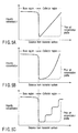
- FIGS. 5A to 5C are impurity-concentration profiles of a bipolar transistor in its depth direction.
- the second embodiment is directed to an improvement of impurity-concentration profiles in the bipolar transistor of the first embodiment.
- the impurity concentration of the collector region increases linearly in its depth direction.
- FIG. 5B it increases almost quadratically.
- FIG. 5C it increases stepwise in more steps than those in the first embodiment.
- the impurity-concentration profile is set such that the impurity concentration increases in the depth direction
- the variations of the width of the depletion layer can be reduced as the reversed bias applied between the base and collector regions becomes high.
- the variations of the parasitic capacitance due to the applied bias can be suppressed while keeping the base-to-collector parasitic capacitance at the same level as that of the prior art bipolar transistor.
- the impurity-concentration profiles are not limited to those described above. Impurity concentrations, which increase as a higher-order (quadric or more) function or an exponential function, can be adopted, provided they increase in the depth direction. Since the impurity-concentration profiles do not influence the parasitic capacitance except where the depletion layer expands, it is possible to provide a region in which the impurity concentration lowers without any problems of impedance.
- the above impurity-concentration profiles can be formed by ion implantation or epitaxial growth in which the impurity concentration varies step by step.
- FIG. 6 is a block diagram of part of the PHS terminal.
- the PHS terminal comprises a radio unit 20 and a modem unit 30.
- the radio unit 20 includes an antenna 21, a radio-frequency switch (SW) 22, a receiving section 23, a transmission section 24, a synthesizer 25, and a temperature sensor 26.
- SW radio-frequency switch
- the antenna 21 receives a radio carrier signal from a base station (not shown) and then supplies it to the reception section 23 through the radio-frequency switch 22 of the radio unit 20.
- the radio carrier signal is mixed with a reference oscillation signal generated from the synthesizer 25 and then down-converted to a receiving intermediate-frequency signal.
- the intermediate-frequency signal is supplied from the reception section 23 to a demodulation section 31 of the modem unit 30.
- the demodulation section 31 digitally demodulates the intermediate-frequency signal to reproduce a digital demodulation signal.
- the digital demodulation signal is separated into data for each reception time slot.
- the data is packet data or control data, it is analyzed by a data communication section (not shown) and displayed on a display section of the PHS.
- the data is voice data, it is decoded by a call unit (not shown) and converted into an analog signal, and the analog signal is output from a speaker.
- a voice signal of a user of the PHS terminal which is supplied from a microphone, is subjected to PCM (Pulse Code Modulation) coding and compression coding in the call unit (not shown).
- PCM Pulse Code Modulation
- the coded voice data and the control data and packet data supplied from the data communication section are multiplexed and input to a modulation section 32 of the modem unit 30.
- the modulation section 32 digitally modulates a transmitting intermediate-frequency signal by the input multiplexed digital communication signal and supplies the modulated intermediate-frequency signal to the transmission section 24.
- the modulated intermediate-frequency signal is mixed with the reference oscillation signal generated from the synthesizer 25 and up-converted to a radio carrier frequency.
- the up-converted signal is amplified to a given transmission/reception power level.
- a radio carrier signal output from the transmission section 24 is transmitted to the base station (not shown) from the antenna 21 via the radio-frequency switch 22.
- the temperature sensor 26 in the radio unit 20 corrects an oscillation frequency of a reference oscillator (REF) 40 provided in the synthesizer 25 in accordance with ambient temperatures.
- REF reference oscillator
- FIG. 7 illustrates an example of the circuit arrangement of the reference oscillator 40.
- a resistance element Rc, npn bipolar transistors Tr1 and Tr2, and a resistance element RE are connected in series between a power supply potential Vcc and a ground potential GND.
- Resistance elements R1 to R3, which serve as bias resistors of the transistors Tr1 and Tr2, are connected in parallel with the resistance element Rc, transistors Tr1 and Tr2, and a resistance element R E .
- An LC oscillation circuit is connected to the base of the transistor Tr2.
- the LC oscillation circuit includes a capacitor C1 and an inductor L connected in series and capacitors C2 and C3 connected in series.
- a connection node between the capacitors C2 and C3 is connected to a connection node between the emitter of the transistor Tr2 and the resistance element R E .
- the connection node between the capacitors C2 and C3 is also connected to a connection node between the resistance elements R1 and R2 through a capacitor C4.
- a capacitor C5 is connected between the ground potential GND and a connection node between the emitter of the transistor Tr1 and the collector of the transistor Tr2.
- a connection node between the collector of the transistor Trl and the resistance element Rc serves as an output terminal.
- the reference oscillator so constituted generates a reference oscillation signal that is required when the radio carrier signal is down-converted into a receiving intermediate-frequency signal or when the transmitting intermediate-frequency signal is up-converted into a radio carrier signal.
- a precise oscillation frequency and a high degree of reliability are needed for the reference oscillator.
- the importance in this case is parasitic capacitance between the base and collector of the bipolar transistor Tr2.
- the power supply for supplying the power supply potential Vcc is mainly a battery. The power supply potential Vcc therefore drops due to a call and data communications. If the base-to-collector capacitance of the bipolar transistor Tr2 is varied with a change of the power supply potential Vcc, the oscillation frequency is varied.
- the foregoing structures of the first and second embodiments are applied to the bipolar transistor Tr2 constituting the reference oscillator.
- the power supply potential Vcc in itself is set low by request for low-voltage driving.
- the condition of normal operations of the bipolar transistor Tr2 is expressed as follows: Vbc is almost equal to 0V or Vbe is equal to Vce.
- the width of a depletion layer formed in the collector region is about 300 ⁇ under conditions that the impurity concentration of the low-concentration collector region is 1.5 x 10 16 cm -2 and Vbc is equal to 0V.
- the thickness of the low-concentration collector region has only to be set at 300 ⁇ or less.
- the variations of parasitic capacitance due to a decrease of the power supply potential Vcc can be suppressed while keeping the base-to-collector parasitic capacitance at the same level as that of the parasitic capacitance in the prior art, and the operation reliability of the reference oscillator can be improved, as can be that of the PHS terminal.
- the present invention is not limited to the above embodiments but can widely be applied to devices in which the parasitic capacitance depending upon a depletion layer formed at a pn junction becomes a problem.
- the bipolar transistors of the above embodiments are used not only in PHS terminals but also in all oscillation circuits constituted using bipolar transistors.
- the above-described present invention provides a semiconductor device that is capable of suppressing variations of the depth of a depletion layer due to an applied voltage while decreasing the parasitic capacitance at a pn junction.
Landscapes
- Bipolar Transistors (AREA)
- Bipolar Integrated Circuits (AREA)
- Inductance-Capacitance Distribution Constants And Capacitance-Resistance Oscillators (AREA)
Applications Claiming Priority (2)
| Application Number | Priority Date | Filing Date | Title |
|---|---|---|---|
| JP2000199841 | 2000-06-30 | ||
| JP2000199841A JP3730483B2 (ja) | 2000-06-30 | 2000-06-30 | バイポーラトランジスタ |
Publications (2)
| Publication Number | Publication Date |
|---|---|
| EP1168452A2 true EP1168452A2 (de) | 2002-01-02 |
| EP1168452A3 EP1168452A3 (de) | 2004-10-06 |
Family
ID=18697790
Family Applications (1)
| Application Number | Title | Priority Date | Filing Date |
|---|---|---|---|
| EP20010114890 Withdrawn EP1168452A3 (de) | 2000-06-30 | 2001-06-29 | Halbleiterbauelement mit vertikalem Bipolartransistor |
Country Status (4)
| Country | Link |
|---|---|
| US (1) | US6472713B2 (de) |
| EP (1) | EP1168452A3 (de) |
| JP (1) | JP3730483B2 (de) |
| KR (1) | KR20020002274A (de) |
Cited By (3)
| Publication number | Priority date | Publication date | Assignee | Title |
|---|---|---|---|---|
| WO2005098960A3 (de) * | 2004-04-02 | 2006-04-20 | Prema Semiconductor Gmbh | Bipolar-transistor und verfahren zur herstellung eines bipolar-transistors |
| EP1801884A3 (de) * | 2005-12-22 | 2009-08-26 | Panasonic Corporation | BipolarerHeteroübergangstransistor und Herstellungsverfahren davon |
| WO2018127514A1 (en) * | 2017-01-03 | 2018-07-12 | Technische Universiteit Delft | Active semiconductor device with linearized junction capacitance |
Families Citing this family (2)
| Publication number | Priority date | Publication date | Assignee | Title |
|---|---|---|---|---|
| US8928142B2 (en) * | 2013-02-22 | 2015-01-06 | Fairchild Semiconductor Corporation | Apparatus related to capacitance reduction of a signal port |
| US11609128B2 (en) * | 2019-12-10 | 2023-03-21 | Wiliot, LTD. | Single layer LC oscillator |
Family Cites Families (7)
| Publication number | Priority date | Publication date | Assignee | Title |
|---|---|---|---|---|
| US3341755A (en) * | 1964-03-20 | 1967-09-12 | Westinghouse Electric Corp | Switching transistor structure and method of making the same |
| US3964089A (en) * | 1972-09-21 | 1976-06-15 | Bell Telephone Laboratories, Incorporated | Junction transistor with linearly graded impurity concentration in the high resistivity portion of its collector zone |
| US4266238A (en) * | 1977-03-11 | 1981-05-05 | Zaidan Hojin Handotai Kenkyu Shinkokai | Semiconductor device having high-speed operation and integrated circuit using same |
| US4593305A (en) | 1983-05-17 | 1986-06-03 | Kabushiki Kaisha Toshiba | Heterostructure bipolar transistor |
| ES2152919T3 (es) * | 1990-01-08 | 2001-02-16 | Harris Corp | Procedimiento de utilizacion de un dispositivo semiconductor que comprende un sustrato que tiene un islote semiconductor dielectricamente aislado. |
| DE69331052T2 (de) * | 1993-07-01 | 2002-06-06 | Consorzio Per La Ricerca Sulla Microelettronica Nel Mezzogiorno, Catania | Integrierte Randstruktur für Hochspannung-Halbleiteranordnungen und dazugehöriger Herstellungsprozess |
| WO1999040630A2 (en) * | 1998-02-09 | 1999-08-12 | Koninklijke Philips Electronics N.V. | Semiconductor device with a bipolar transistor, and method of manufacturing such a device |
-
2000
- 2000-06-30 JP JP2000199841A patent/JP3730483B2/ja not_active Expired - Fee Related
-
2001
- 2001-06-28 KR KR1020010037536A patent/KR20020002274A/ko not_active Ceased
- 2001-06-28 US US09/892,447 patent/US6472713B2/en not_active Expired - Fee Related
- 2001-06-29 EP EP20010114890 patent/EP1168452A3/de not_active Withdrawn
Cited By (6)
| Publication number | Priority date | Publication date | Assignee | Title |
|---|---|---|---|---|
| WO2005098960A3 (de) * | 2004-04-02 | 2006-04-20 | Prema Semiconductor Gmbh | Bipolar-transistor und verfahren zur herstellung eines bipolar-transistors |
| US7563685B2 (en) | 2004-04-02 | 2009-07-21 | Prema-Semiconductor GmbH | Bipolar-transistor and method for the production of a bipolar-transistor |
| EP1801884A3 (de) * | 2005-12-22 | 2009-08-26 | Panasonic Corporation | BipolarerHeteroübergangstransistor und Herstellungsverfahren davon |
| US7728357B2 (en) | 2005-12-22 | 2010-06-01 | Panasonic Corporation | Heterojunction bipolar transistor and manufacturing method thereof |
| WO2018127514A1 (en) * | 2017-01-03 | 2018-07-12 | Technische Universiteit Delft | Active semiconductor device with linearized junction capacitance |
| NL2018115B1 (en) * | 2017-01-03 | 2018-07-25 | Univ Delft Tech | Active semiconductor device with linearized depletion capacitance |
Also Published As
| Publication number | Publication date |
|---|---|
| US20020000574A1 (en) | 2002-01-03 |
| JP2002026028A (ja) | 2002-01-25 |
| JP3730483B2 (ja) | 2006-01-05 |
| US6472713B2 (en) | 2002-10-29 |
| KR20020002274A (ko) | 2002-01-09 |
| EP1168452A3 (de) | 2004-10-06 |
Similar Documents
| Publication | Publication Date | Title |
|---|---|---|
| US6355961B1 (en) | Structure and method for improved signal processing | |
| US6100770A (en) | MIS transistor varactor device and oscillator using same | |
| US5949104A (en) | Source connection structure for lateral RF MOS devices | |
| Porret et al. | Design of high-Q varactors for low-power wireless applications using a standard CMOS process | |
| US5396132A (en) | MESFET mixer circuit having a pulse doped structure | |
| EP0646965B1 (de) | Eine integrierte Vorrichtung mit einem bipolaren Transistor und einem MOSFET Transistor in Emittorschaltungsanordnung | |
| US20020063270A1 (en) | High frequency switch circuit device | |
| US20030096481A1 (en) | Self-alignment of seperated regions in a lateral MOSFET structure of an integrated circuit | |
| US8766735B2 (en) | Low power voltage controlled oscillator | |
| EP1168452A2 (de) | Halbleiterbauelement mit vertikalem Bipolartransistor | |
| EP1058949B1 (de) | Rf-mos-transistor | |
| Schüppen et al. | Mesa and planar SiGe-HBTs on MBE-wafers | |
| EP0902483B1 (de) | Elektrische Anordnung mit einer spannungsabhängiger Kapazität und Verfahren zur Herstellung | |
| EP1261025B1 (de) | Halbleiterbauelement und dessen Herstellungsverfahren | |
| US6984869B2 (en) | High performance diode implanted voltage controlled p-type diffusion resistor | |
| US7081799B2 (en) | Bipolar transistor, oscillation circuit, and voltage controlled oscillator | |
| US6707115B2 (en) | Transistor with minimal hot electron injection | |
| US7205837B2 (en) | Body effect amplifier | |
| KR100707877B1 (ko) | 낮은 분산의 용량성 네트워크를 포함하는 집적 회로 및 관련된 무선 신호 수신기 | |
| US20050212048A1 (en) | Integrated switch device | |
| JPH0797553B2 (ja) | Npnトランジスタ−の固有降伏電圧より大きい降伏電圧を有するnpn等価構造 | |
| US6020623A (en) | Integrated structure with device having a preset reverse conduction threshold | |
| US20060033183A1 (en) | Cascode, cascode circuit and method for vertical integration of two bipolar transistors into a cascode arrangement | |
| US5708398A (en) | Dual voltage controlled oscillator using integrated transistor and negative differential resistance diode | |
| WO2001095396A3 (en) | Double-implant high performance varactor and method for manufacturing same |
Legal Events
| Date | Code | Title | Description |
|---|---|---|---|
| PUAI | Public reference made under article 153(3) epc to a published international application that has entered the european phase |
Free format text: ORIGINAL CODE: 0009012 |
|
| 17P | Request for examination filed |
Effective date: 20010629 |
|
| AK | Designated contracting states |
Kind code of ref document: A2 Designated state(s): AT BE CH CY DE DK ES FI FR GB GR IE IT LI LU MC NL PT SE TR |
|
| AX | Request for extension of the european patent |
Free format text: AL;LT;LV;MK;RO;SI |
|
| PUAL | Search report despatched |
Free format text: ORIGINAL CODE: 0009013 |
|
| AK | Designated contracting states |
Kind code of ref document: A3 Designated state(s): AT BE CH CY DE DK ES FI FR GB GR IE IT LI LU MC NL PT SE TR |
|
| AX | Request for extension of the european patent |
Extension state: AL LT LV MK RO SI |
|
| AKX | Designation fees paid |
Designated state(s): DE FR NL |
|
| 17Q | First examination report despatched |
Effective date: 20081230 |
|
| STAA | Information on the status of an ep patent application or granted ep patent |
Free format text: STATUS: THE APPLICATION IS DEEMED TO BE WITHDRAWN |
|
| 18D | Application deemed to be withdrawn |
Effective date: 20150731 |