EP1168645A2 - Circuit émetteur-récepteur - Google Patents
Circuit émetteur-récepteur Download PDFInfo
- Publication number
- EP1168645A2 EP1168645A2 EP01109681A EP01109681A EP1168645A2 EP 1168645 A2 EP1168645 A2 EP 1168645A2 EP 01109681 A EP01109681 A EP 01109681A EP 01109681 A EP01109681 A EP 01109681A EP 1168645 A2 EP1168645 A2 EP 1168645A2
- Authority
- EP
- European Patent Office
- Prior art keywords
- voltage
- components
- control logic
- transmit
- supply voltage
- Prior art date
- Legal status (The legal status is an assumption and is not a legal conclusion. Google has not performed a legal analysis and makes no representation as to the accuracy of the status listed.)
- Granted
Links
Images


Classifications
-
- H—ELECTRICITY
- H04—ELECTRIC COMMUNICATION TECHNIQUE
- H04B—TRANSMISSION
- H04B1/00—Details of transmission systems, not covered by a single one of groups H04B3/00 - H04B13/00; Details of transmission systems not characterised by the medium used for transmission
- H04B1/38—Transceivers, i.e. devices in which transmitter and receiver form a structural unit and in which at least one part is used for functions of transmitting and receiving
- H04B1/40—Circuits
-
- H—ELECTRICITY
- H04—ELECTRIC COMMUNICATION TECHNIQUE
- H04B—TRANSMISSION
- H04B1/00—Details of transmission systems, not covered by a single one of groups H04B3/00 - H04B13/00; Details of transmission systems not characterised by the medium used for transmission
- H04B1/06—Receivers
- H04B1/16—Circuits
- H04B1/1607—Supply circuits
- H04B1/1615—Switching on; Switching off, e.g. remotely
-
- H—ELECTRICITY
- H04—ELECTRIC COMMUNICATION TECHNIQUE
- H04W—WIRELESS COMMUNICATION NETWORKS
- H04W52/00—Power management, e.g. Transmission Power Control [TPC] or power classes
- H04W52/02—Power saving arrangements
- H04W52/0209—Power saving arrangements in terminal devices
- H04W52/0261—Power saving arrangements in terminal devices managing power supply demand, e.g. depending on battery level
- H04W52/0274—Power saving arrangements in terminal devices managing power supply demand, e.g. depending on battery level by switching on or off the equipment or parts thereof
- H04W52/028—Power saving arrangements in terminal devices managing power supply demand, e.g. depending on battery level by switching on or off the equipment or parts thereof switching on or off only a part of the equipment circuit blocks
-
- Y—GENERAL TAGGING OF NEW TECHNOLOGICAL DEVELOPMENTS; GENERAL TAGGING OF CROSS-SECTIONAL TECHNOLOGIES SPANNING OVER SEVERAL SECTIONS OF THE IPC; TECHNICAL SUBJECTS COVERED BY FORMER USPC CROSS-REFERENCE ART COLLECTIONS [XRACs] AND DIGESTS
- Y02—TECHNOLOGIES OR APPLICATIONS FOR MITIGATION OR ADAPTATION AGAINST CLIMATE CHANGE
- Y02D—CLIMATE CHANGE MITIGATION TECHNOLOGIES IN INFORMATION AND COMMUNICATION TECHNOLOGIES [ICT], I.E. INFORMATION AND COMMUNICATION TECHNOLOGIES AIMING AT THE REDUCTION OF THEIR OWN ENERGY USE
- Y02D30/00—Reducing energy consumption in communication networks
- Y02D30/70—Reducing energy consumption in communication networks in wireless communication networks
Definitions
- the present invention relates to transmission / reception circuits and in particular to transmission / reception circuits for cordless telephones, data transmission devices such as e.g. Data transmission devices of the DECT and Bluetooth standards, mobile phones, such as GSM, DCS, PCS mobile phones, and ISM band data transfers.
- data transmission devices such as e.g. Data transmission devices of the DECT and Bluetooth standards
- mobile phones such as GSM, DCS, PCS mobile phones, and ISM band data transfers.
- the power consumption during operation of the transmission / reception circuit is reduced by using entire systems, which comprise several blocks, e.g. Send or receive path, included, switched on or off or put into a standby mode.
- entire systems which comprise several blocks, e.g. Send or receive path, included, switched on or off or put into a standby mode.
- a mixer, an intermediate frequency amplifier and a frequency modulation detection circuit or an FM detector can be deactivated during transmission.
- a transmission output stage and a preamplifier can be switched off during a reception process.
- the synthesizer or the frequency generation circuit is required both during the transmission and the reception process and can consequently only be put into a standby (standby) operating state if neither transmission nor reception is carried out.
- some currently available transmission / reception circuits have a continuous, dynamic control of the amplification of the intermediate frequency amplifier and of the transmission output stage, which are dynamically regulated during operation.
- RSSI Receive Signal Strength Indicator
- AGC Automatic Gain Control
- a disadvantage of the existing transmit / receive systems is that many function blocks are oversized for the actual tasks during operation and consequently require too much power loss. The reason for this is that the individual components must be designed for the worst reception and transmission conditions, i.e. for the "worst case" case with maximum adjacent channel interference and minimal reception power.
- the received signal strength can vary, for example, between -94 dBm and +10 dBm, with the received power minimum value of -94 dBm being reached only in the rarest of cases.
- the adjacent channel interferers rarely reach the maximum values specified in the specifications, if they exist at all.
- the object of the present invention is one To create transmit / receive circuit in which the operating power consumption is lower.
- a transmission / reception circuit has a plurality of electronic components which are connected in order to cooperate for the transmission and reception of data, the components being controllable by control signals.
- the transmit / receive circuit also has control logic, which is connected to the plurality of electronic components, for monitoring current operating parameters of the transmit / receive circuit and for outputting control signals to the plurality of electronic components depending on the current operating parameters, the control signals being at the components comprise at least two parameters from a group of parameters consisting of the supply voltage, the amplification, a filter selection and a clock speed with which at least one of the components is operated.
- a transmission / reception circuit comprises a transmission part, a reception part and a synthesizer circuit or frequency generation circuit.
- the control logic controls a plurality of voltage regulators via voltage signals depending on the received signal strength or similar signals, such as, for example, battery charge status information, received signal interference information and signals from a baseband processor, which are connected to corresponding electronic components of the transmit / receive circuit.
- the transmit / receive circuit further comprises a plurality of intermediate frequency filters, from which the control logic can select a filter which is adapted to the current operating parameters and which, on the one hand, has a sufficiently narrow frequency bandwidth and, on the other hand, the lowest possible insertion loss.
- the signal / receive circuit uses the received signal strength as the current operating parameters, Battery level information, receive signal interference information, and signals from a baseband processor, indicating whether there is a transmit or receive operation to control the electronic components such that the supply voltage and gain reduce in response to an increase in input signal strength, the supply voltage and gain in response a decrease in the battery state of charge is further reduced, a filter with a lower insertion loss and a wider pass frequency band is selected when reception signal interference decreases, and the clock speed is reduced in response to a decrease in the data rate transmission rate.
- Voltage regulators such as linear and switching regulators are used to control the amplification and the supply voltage.
- An advantage of the present invention is that by using the current operating parameters, e.g. the reception conditions or the battery charge state, an adapted operating state of the transmission / reception circuit can be ensured.
- the individual subsystems e.g. activate or deactivate the transmission or reception path, or only dynamically regulate the intermediate frequency amplifier or the transmission output stage, in the present invention, through the dynamic control, configuration and supply of individual components in accordance with the current operating parameters during operation, a highly efficient, performance-optimized operation of the total transmission / reception circuit achieved.
- the separate power supply of the individual electronic components of the circuit by means of the various voltage regulators ensures that all components are decoupled.
- strong changes in load such as the switching on or off of one or more components, do not have the effect of a fluctuation in the supply voltage, as is the case when the electronic Components would be connected directly to the same power supply.
- the voltage regulators can be used to place the electronic components in a standby mode, in which no supply voltage is supplied to the electronic components, and consequently leakage currents are avoided, and the voltage regulators themselves require a minimal supply current. In this way, the operating time of a battery-operated transceiver unit can be extended.
- the transmission / reception circuit which intelligently, dynamically supplies, controls and configures the individual electronic components, (a) the operating time of a battery-operated transmitting / receiving unit can be extended, (b) the operating capacity of the battery and thus its maximum capacity Volume or their weight is reduced, and (c) the power loss consumed in the transmitter / receiver unit is reduced, and in turn the expensive heat sink is reduced, as a result of which the total volume of a device containing the transmitter / receiver circuit can be reduced.
- a transmission / reception circuit is designed according to current operating parameters, e.g. Ambient conditions or reception conditions, or intelligently supplied, controlled and configured according to the resulting requirements.
- current operating parameters e.g. Ambient conditions or reception conditions
- intelligently supplied controlled and configured according to the resulting requirements.
- a minimal power consumption is always guaranteed.
- this supply, control and configuration is carried out by a power management module which consists of control logic, a plurality of digitally adjustable linear and switching regulators and a variable clock generator.
- the control logic reads in signals that characterize the requirements for the overall system or the current operating parameters.
- control signals are then generated and output in accordance with these signals, which ensure low-power, optimized operation of the individual system blocks or of the individual electronic components and of the entire system.
- These control signals regulate the output voltages of the adjustable linear and switching regulators and thus control the supply and indirectly the function of the individual blocks.
- SAW intermediate frequency surface wave
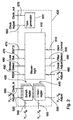
- the mixer 50 mixes the signal received by the antenna 10, filtered by the RF filter 20 and amplified by the low noise input amplifier LNA 40 during a reception process with a signal which it receives from a synthesizer circuit 120.
- the synthesizer circuit 120 is connected to the mixer 50 via a transmit (TX) filter 130, a transmit / receive (T / R) switch 140 and a phase shifter 150, which are connected in series.
- the synthesizer circuit 120, the transmission filter 130, the T / R switch 140, a preamplifier 160, a transmission filter 170, a power amplifier (PA) are a in the transmission / reception circuit of FIG Output matching filter 190, T / R switch 30, RF filter 20 and antenna 10 connected in series.
- the synthesizer circuit 120 comprises two inputs 200 and 210, ie a transmit (TX) data input 210 and a PLL-TX control bus input.
- the synthesizer circuit 120 further includes a compensation circuit 220, a transmit (TX) data filter 230, a phase lock circuit PLL 240 with a phase detector, a loop filter 250, a voltage controlled oscillator 260 and a frequency doubler 270.
- the transmit data filter 230 and the compensation circuit 220 is connected to the transmission data input 210 in order to receive the data to be transmitted via the same.
- the oscillator 260 is connected to the compensation circuit 220 via the loop filter 250 and the PLL 240.
- the oscillator 260 is via a feedback path also connected directly to the PLL 240 to form a phase locked loop with the loop filter 250 and the PLL.
- the PLL 240 is also connected at one of its inputs to the PLL-TX control bus input 200, via which it receives input control signals for the phase-locked loop.
- the oscillator 260 is also connected to the transmit data filter 230 to receive filtered transmit data therefrom.
- the output of the oscillator 260 is connected to the frequency Doppler 270, which in turn is connected to the transmission filter 130 and outputs the output signal of the synthesizer circuit 120.
- the transmit / receive circuit of FIG. 1 is supplied by a battery voltage V b . While some components of the transmit / receive circuit of FIG. 1 are powered directly by the battery voltage V b , some components are powered by separate voltage regulators.
- the low-noise input amplifier LNA 40, the power amplifier and the transmission output stage PA 180, the two intermediate frequency amplifiers IF-Amp1 + IF-Amp2 80 and 90, the voltage-controlled oscillator VCO 260 and the digital components of the synthesizer circuit 120 , ie the frequency doubler 270, the TX data filter 230, the compensation circuit 220 and the PLL 240 with the phase detector, are supplied by separate voltage regulators, which in turn are connected to the battery voltage V b .
- the bias voltage or the input bias of the LNA 40 and the PA 180 are further Voltage regulator 333 or 336 regulated.
- voltage regulators 280-310 and 330-336 are connected to battery voltage V b and each have an adjustment input.
- the adjust input of the voltage regulators 280-310 and 330-336 is used, as will be described in the following, to set the supply voltages or the bias voltage and thus the function of the corresponding electronic components in accordance with certain current operating parameters of the transmit / receive circuit.
- a selected filter 70 is connected in series in the reception path of the transmission / reception circuit.
- a selector circuit selects a suitable filter from a plurality of filters 70a and 70b in accordance with certain instantaneous operating parameters of the transmitting / receiving circuit.
- this selector circuit has an input Filter Select 340.
- the RSSI value ie the received signal strength
- LNA 40 the low-noise input amplifier
- VCO 260 the power amplifier 180 and the intermediate frequency amplifiers 80 and 90
- the LNA 40 can be regulated via its supply voltage or via the input bias (bias voltage). By reducing this voltage, the gain is reduced and the power loss is reduced.
- the control of the supply voltage is carried out via the voltage regulator 280 and the control of the bias voltage via the voltage regulator 333, both of which are dynamically adjustable DC-DC converters (DC-DC converters).
- the voltage regulator 280 is also used to place the LNA 40 in a standby mode. During standby mode, the LNA 40 is deactivated by interrupting its supply voltage. This avoids leakage currents that would normally arise during the actual standby operation of the LNA 40, ie if it were directly connected to the battery voltage V b .
- the voltage regulator 280 has its own standby operating state, in which it requires only a minimal supply current.
- the power amplifier 180, the intermediate frequency amplifiers 80 and 90 and the oscillator 260 are supplied by a voltage regulator 290, 300 and 310 with the lowest possible supply voltage, the power loss being reduced when the supply voltage is reduced and in a standby mode Leakage currents can be avoided.
- An advantage of using separate voltage regulators 280-310 and 330 for the individual components is that the individual components are thereby decoupled from one another. Supply voltage fluctuations, which would be caused by strong load changes, such as switching on or off one or more components, if all function blocks or electronic components without a controller directly with the same supply voltage would be avoided by this decoupling. Since these fluctuations also influence the actual receive and transmit signals, the signal-to-noise ratio is consequently improved.
- the VCO 260 oscillator can be controlled directly via its supply voltage. With a strong input signal, i.e. a high RSSI value, a higher phase noise of the oscillator 260 can be tolerated. Interferers or interference frequencies are mixed more strongly into the reception band, but this is harmless if the desired signal is sufficiently high.
- the power amplifier or the transmitting output stage can also be controlled by means of the RSSI value via its supply voltage, which is supplied by the voltage regulator 290, or via its bias voltage, which is supplied by the voltage regulator 336.
- the consideration of using the received signal strength to regulate the output gain is that it is assumed that a high RSSI value suggests a good radio connection to the opposite station or base station (not shown) and consequently the transmission power can be reduced ,
- a second RSSI measurement before the intermediate frequency filter 70 and a comparison with the actual RSSI value, which is measured after this filter 70, and a comparison of the two values can be used to infer the presence of interferers or interference frequencies.
- a broadband filter 70 can be selected from the plurality of filters 70a and 70b with a lower insertion loss via the control line Filter Select 340, as will be described below, thereby reducing the subsequent gain and power consumption can.
- the supply voltage of the digital components 320 of the Synthesizers 120 ie the frequency doubler 270, the transmit data filter 230, the compensation circuit 220 and the phase lock circuit 240, cannot be reduced directly, since the correct functioning of a digital circuit can no longer be guaranteed above a certain minimum voltage.
- the clock for the digital components is reduced if the performance is reduced or the capacity is reduced, since the switching delay caused by a reduction in the supply voltage can be tolerated due to the lower processing speed when the clock is reduced.
- the mixer supply could also be reduced when the input signal is high and the power consumption of the mixer reduced.
- the power management module 400 includes one Logic circuit 410, a clock generator 420, a plurality of switching regulators 430 and a plurality of linear regulators 440.
- the switching regulators 430 and linear regulators 440 correspond to the voltage regulators 280-310 and 330-336 shown in FIG. 1, it being noted that in the choice Which voltage regulator 280-310 and 330-336 is a switching regulator or a linear regulator, especially the efficiency and the output noise as well as the transient response must be considered.
- the voltage regulators 280 and 310 are preferably designed as linear regulators, since they have to take care of a low noise of the supply voltage. The same approach is used to select the other DC-DC converters.
- the control logic 410 of FIG. 2 has four inputs 450, 460, 470 and 475, in which the control logic 410 has four different instantaneous operating parameters, ie the received signal strength RSSI, received signal interference information (blocker detect), battery charge status information (low. Bat) and receives information about whether there is a transmission or a reception process, which are explained in more detail below.
- the control logic 410 Based on the current operating parameters received, the control logic 410 generates corresponding control signals which it outputs at a plurality of outputs 480, two outputs 490 and 500 and a plurality of outputs 510.
- the plurality of outputs 480 and 510 are connected to the plurality of voltage regulators 430 and 440 at their respective inputs 520 and 530, respectively.
- control logic 410 can control the supply voltages or the bias voltages of electronic components of the transmit / receive circuit are connected to outputs 540 and 550 of the plurality of voltage regulators 430 and 440, respectively, in such a way that the total power consumption of the transmitting / receiving circuit is reduced or minimized in accordance with the current operating parameters.
- the output 490 (clock adjust) is connected to an input 560 of the clock generator 420, which outputs an output 570 for the digital circuit components of the transmit / receive circuit (320 in FIG. 1).
- the plurality of switching regulators 430 also have an input Clock_in 580, via which they receive an internal clock for controlling the output voltage.
- the control logic 410 outputs a signal which, as will be explained in more detail below, depends on the input signals at the inputs 450-475 from the plurality of filters 70a and 70b (FIG. 1), a tolerable filter with less Select insertion loss.
- the operation of the control logic 410 will be described in more detail using a specific example, it is pointed out that, although only seven voltage regulators are shown in FIG. 1, the power management module 400 may include more or fewer voltage regulators that are suitable electronic components of the transmission / reception circuit are connected.
- 3 shows a dashed line voltage management module 600 that includes control logic 610 shown with a dashed line, a plurality of voltage regulators 620, 625, 630, 635, 640, 650, 660 and 670, and a clock generator 690.
- the control logic 610 comprises a plurality of control logic units 700, 710, 720, 730 and 740 and a correction circuit 750.
- the voltage management module comprises 600 of FIG. 3 four inputs Bat_IN, BLD_IN, RSSI_IN and RX / TX 760, 770, 780 and 785.
- the voltage management module 600 also includes ten outputs 790, 795, 800, 805, 810, 820, 830, 840, 850 and 860 ,
- control logic 610 The operation of the control logic 610 and the wiring of the voltage management module 600 and the connection of the outputs 790-860 to the respective electronic components of the transmission / reception circuit of FIG. 1 will now be described below.
- the LNA control logic unit 700 has an input connected to the RSSI_IN input of the voltage management module 600 in order to receive a value for the received signal strength.
- the LNA control logic unit 700 has an output connected to the LNA voltage regulator 620, which in turn is connected to the output LNA_OUT and outputs the supply voltage there to the low-noise input amplifier LNA 40 from FIG. 1.
- the LNA control logic unit 700 is connected at a further output to the voltage regulator 625, which in turn is connected to the output LNA_Bias and outputs the bias voltage to the low-noise input amplifier LNA 40 there.
- Control logic unit 700 is designed to, depending on the RSSI value received, output control signals to voltage regulators 620 and 625 such that they decrease the supply voltage and bias voltage for LNA 40 as the RSSI value increases. This takes into account that a high input signal strength requires less amplification. As a result, the gain is reduced and the power loss is reduced in order to save the power consumption by reducing the supply voltage and the bias voltage. In the present example, the supply voltage and the bias voltage are reduced in such a way that the lowest possible but sufficient amplification value results with low noise at the same time. However, it can be provided that either the supply voltage or the bias voltage of the LNA 40 is controlled and not both, in which case either the voltage regulator 625 (or 333 in FIG. 1) or the voltage regulator 620 (or 280 in FIG. 1) could be missing.
- the control logic unit 700 is also designed to put the LNA into a standby mode, e.g. if the transmission / reception circuit is in a transmission process.
- the LNA control logic unit 700 is connected to the input RX / TX 785, at which it receives a signal from a baseband processor (not shown) which indicates whether there is a transmission or reception process. If the LNA control logic unit 700 puts the LNA into a standby mode, the LNA control logic unit 700 outputs a corresponding control signal to the voltage regulator 620, which then generates 0 volts at its output and then is in its own standby or standby operating state is located, in which the standby mode requires only a minimal supply current.
- the LNA 40 (FIG. 1) is deactivated by interrupting the supply voltage.
- the advantage is that all leakage currents that would normally arise in the actual standby mode of the LNA 40 with an uninterrupted supply voltage are avoided.
- an MX control logic unit 710 is provided in the voltage management module 600 of FIG. 3, which is connected at one input to the RSSI_IN input 780 in order to receive the RSSI value, and at an output to the MXI Voltage regulator 630 is connected.
- the MX voltage regulator 630 is in turn connected to the intermediate frequency mixer 50 via the MX_OUT 800 output.
- the MX control logic unit 710 is designed to set the supply voltage of the mixer 50 according to the RSSI value via the MX voltage regulator 630.
- the MX control logic unit 710 reduces the mixer 50 supply voltage at a higher input signal strength value. For this purpose, the control logic 710 issues a corresponding control signal to the voltage regulator 630.
- the MX control logic unit provides a reduction in the gain and power consumption of the mixer 50 and thus a reduction in the total power consumption.
- the MX control logic 710 also performs the task of placing the mixer 50 in a standby mode when there is a transmit, as described above with reference to the LNA control logic unit.
- the control logic unit 710 like the LNA control logic unit 700, is connected to the input RX / TX in addition to the input RSSI_IN in order to receive information about the presence of a receiving or transmitting operation.
- the PA control logic unit 720 receives the RSSI value at an input from the input RSSI_IN 780 in order to output control signals to the PA voltage regulator 640 or the voltage regulator 635 at two outputs.
- the PA voltage regulator 640 is connected to the power amplifier PA 180 via the output PA_OUT 810 in order to supply the same with the supply voltage in accordance with the control signal from the PA control logic unit 720.
- the voltage regulator 635 is connected to the power amplifier PA 180 via the output PA_Bias 805 in order to supply the bias voltage to it according to the control signal from the PA control logic unit 720.
- the PA control logic unit 720 is designed to control the voltage regulators 635 and 640 via the control signals in such a way that the power amplifier 180 is supplied with a lower supply voltage and / or bias voltage when the RSSI value is higher.
- This mode of operation is based on the assumption that a high RSSI value indicates a good radio connection to the opposite station or base station (not shown), and consequently the amplification or the transmission power can be reduced.
- only the voltage regulator 635 (or 336 in FIG. 1) or the can also be used for the power management of the PA 180 Voltage regulator 640 (or 290 in FIG. 1) can be provided to regulate either the supply voltage or the bias voltage.
- the PA control logic unit 720 also takes on the task of putting the PA 180 into a standby mode when there is a receive operation.
- the control logic unit 720 is connected to the input RX / TX in addition to the input RSSI_IN in order to receive information about the presence of a reception or transmission process.
- the control logic unit 730 is connected to two inputs of the voltage management module 600, the BLD_IN and the RSSI_IN.
- Noise control logic unit 730 receives a second RSSI value via input BLD_IN, which is measured before intermediate frequency filter 70.
- a correction circuit 750 is connected between the noise control logic unit 730 and the input BLD_IN, which corrects the second RSSI value with the insertion loss of the currently selected filter 70.
- Noise control logic unit 730 has an output connected to VCO voltage regulator 650, which in turn is connected to oscillator VCO via output VCO_OUT 820.
- the noise control logic unit 730 outputs a control signal to the voltage regulator 650 such that the oscillator is supplied with a lower supply voltage by the voltage regulator 650 when the two RSSI values are essentially the same or a higher phase noise is tolerable, and is supplied with a higher supply voltage if the two RSSI values are further apart.
- the noise control logic unit 730 is also designed to further reduce the supply voltage to the VCO if the RSSI value increases because higher signal noise in the oscillator can generally be tolerated with a strong signal input strength. In this case, interferers are mixed more strongly into the reception band, but this is harmless if the desired signal is sufficiently high.
- the noise control logic unit 730 is also designed to output a control signal to the output 840 Filter_Out, which is connected to a selector circuit (not shown in Fig. 1) based on the comparison between the two RSSI values, such that a broadband filter is inserted into the filter Receive path of the transmit / receive circuit is switched if the RSSI values essentially match. Since a broadband filter has a lower insertion loss, this can also reduce power consumption.
- the output of the noise control logic unit 730 which is connected to the Filter_OUT output, is also connected to an input of the correction circuit 750.
- the noise control logic unit 730 is also connected at an output to the IF-Amp voltage regulator 660, which is connected via the output IF-Amp_OUT 830 to the two intermediate frequency amplifiers 80 and 90 (FIG. 1).
- the noise control logic unit 730 is designed to reduce the supply voltage of the intermediate frequency amplifiers 80 and 90 in the event that the RSSI values are essentially the same, since the intermediate frequency amplifiers 80 and 90 have a lower gain because of the broadband filter with lower insertion loss that is possible in this case is made possible. For this purpose, the noise control logic unit 730 in turn outputs a suitable control signal to the voltage regulator 660, and this in turn saves power loss. Like those described above Control logic units 700-720, control logic unit 730 is also connected to input RX / TX 785 in order to obtain information about whether a transmission or reception process is currently taking place, for example the supply voltage of IF-Amp voltage regulator 660 being switched off when a transmission process is present can.
- the control logic unit 740 is connected to the RSSI_IN and RX / TX inputs, and is designed to determine the supply voltage and the clock for the digital components 320, ie the PLL 240, based on the RSSI value and the information from the baseband processor Frequency Doppler 270, the compensation circuit 220 and the TX data filter 230 to set.
- the digital part control logic unit 740 is connected to the voltage regulator 670 at a first output and to the clock generator 690 at a second output.
- the digital part control logic unit 740 sends a corresponding control signal clock generator 690, which indicates that the digital components can be supplied with a reduced clock.
- the clock generator 690 outputs a clock with a lower speed for the digital components at the output CL_dig 850 in accordance with the control signal from the digital part control logic unit 740.
- the supply voltage can also be reduced, since the switching delay caused thereby can be tolerated due to the lower processing speed.
- control logic unit 740 is designed to send a control signal to the voltage regulator 670 in such a case that the digital part 320 (FIG. 1) of the synthesizer circuit 120 is supplied with a lower supply voltage by the voltage regulator 670 via the output Dig_OUT 860, which in turn Power loss is saved.
- the control logic unit 740 is also designed to switch off the supply voltage of any possible individual components depending on the information received from the baseband processor as to whether there is currently a transmission or reception process or neither.
- the BAT_IN 760 input is connected to each control logic unit 700-740 to provide battery charge status information to each control logic unit 700-740.
- the control logic units 700-740 are designed to use this information about the state of charge of the battery (not shown) in addition to the information mentioned above, for example to effect an especially low-loss operating mode while sacrificing the quality of the received data (RX data), to be able to carry out the most important functions of the transmit / receive circuit even when the battery is almost empty.
- FIG. 3 shows a power management module which consists of control logic, a plurality of digitally adjustable linear and switching regulators and a variable clock generator.
- the control logic reads in signals that characterize the requirements for the overall system. In the present case, these are the RSSI signals (RSSI, blocker detected), signals from the baseband processor of the transmission / reception circuit or signals from the battery management system, such as a charge status display or an indication that the charge capacity has fallen below a certain threshold value.
- the logic must process these signals and generate control signals which are then passed on to the adjustable voltage regulators and thus control the output voltages of the same. As a result, the supply voltage is adjusted, and thus indirectly the control of the function of the individual blocks.
- signals for setting the clock frequency, for selecting the filters and for regulating the gains are generated in accordance with the measured input signals of the control logic. In this way, a low-performance, optimized operation of the individual system blocks or electronic components as well as the entire system can be guaranteed.
- control logic can, for example, have further inputs through which it receives further signals from the baseband processor.
- number of outputs can vary, with further or fewer parameters being able to be controlled in accordance with the current operating parameters.
- the present invention is directed to transmit / receive circuits for cordless telephones, data transmission devices such as e.g. Data transmission devices of the DECT and Bluetooth standards, mobile phones, such as GSM, DCS, PCS mobile phones, and ISM band data transmissions applicable.
- control logic units of Fig. 3 are designed by the circuit design to perform the operation described above or that they each additionally have a look-up table in which responses to certain input signals to the control logic units are stored. It is also noted that the control logic may be formed using a single look-up table in which a set of values for each voltage regulator, clock generator and filter selector circuit for each set of input values are stored at the inputs of the control logic and power management module, respectively is.
- control logic units are constructed in analog or digital form.
- control logic units are constructed digitally, digital control signals being output by the control logic units.
- transceiver part of Fig. 1 is not essential to the present invention.
- individual components can be designed differently, e.g. the voltage regulator.
Landscapes
- Engineering & Computer Science (AREA)
- Computer Networks & Wireless Communication (AREA)
- Signal Processing (AREA)
- Transceivers (AREA)
- Mobile Radio Communication Systems (AREA)
- Transmitters (AREA)
- Burglar Alarm Systems (AREA)
- Seal Device For Vehicle (AREA)
- Control Of Motors That Do Not Use Commutators (AREA)
- Input Circuits Of Receivers And Coupling Of Receivers And Audio Equipment (AREA)
- Circuits Of Receivers In General (AREA)
Applications Claiming Priority (2)
| Application Number | Priority Date | Filing Date | Title |
|---|---|---|---|
| DE10027869 | 2000-06-06 | ||
| DE10027869A DE10027869C2 (de) | 2000-06-06 | 2000-06-06 | Sende/Empfangsschaltung |
Publications (3)
| Publication Number | Publication Date |
|---|---|
| EP1168645A2 true EP1168645A2 (fr) | 2002-01-02 |
| EP1168645A3 EP1168645A3 (fr) | 2004-12-29 |
| EP1168645B1 EP1168645B1 (fr) | 2006-12-27 |
Family
ID=7644790
Family Applications (1)
| Application Number | Title | Priority Date | Filing Date |
|---|---|---|---|
| EP01109681A Expired - Lifetime EP1168645B1 (fr) | 2000-06-06 | 2001-04-19 | Circuit émetteur-récepteur |
Country Status (4)
| Country | Link |
|---|---|
| EP (1) | EP1168645B1 (fr) |
| AT (1) | ATE349812T1 (fr) |
| DE (3) | DE10066103C2 (fr) |
| ES (1) | ES2275579T3 (fr) |
Family Cites Families (13)
| Publication number | Priority date | Publication date | Assignee | Title |
|---|---|---|---|---|
| JP2795054B2 (ja) * | 1991-05-31 | 1998-09-10 | 日本電気株式会社 | 携帯電話機 |
| EP0522720B1 (fr) * | 1991-06-18 | 1999-08-18 | Nokia Mobile Phones Ltd. | Réglage de la fréquence d'horloge d'un circuit électrique |
| DE4208605A1 (de) * | 1992-03-18 | 1993-09-23 | Blaupunkt Werke Gmbh | Schaltungsanordnung zur nachbarkanalerkennung und -unterdrueckung in einem rundfunkempfaenger |
| FI96656C (fi) * | 1992-11-27 | 1996-07-25 | Nokia Telecommunications Oy | Radiojärjestelmä |
| DE4319457C2 (de) * | 1993-06-11 | 1997-09-04 | Blaupunkt Werke Gmbh | Schaltungsanordnung zur Nachbarkanalerkennung und -unterdrückung in einem FM-Rundfunkempfänger |
| JPH0818500A (ja) * | 1994-06-30 | 1996-01-19 | Nec Corp | 携帯無線機 |
| KR100346503B1 (ko) * | 1994-07-21 | 2002-11-22 | 인터디지탈 테크날러지 코포레이션 | 통신시스템 가입자 유니트용 전력소비 제어방법 및 장치 |
| JP2766230B2 (ja) * | 1995-10-12 | 1998-06-18 | 埼玉日本電気株式会社 | 受信増幅装置 |
| FI101669B (fi) * | 1996-02-23 | 1998-07-31 | Nokia Mobile Phones Ltd | Monipalvelumatkaviestin |
| WO1998012822A1 (fr) * | 1996-09-18 | 1998-03-26 | Siemens Aktiengesellschaft | Procede et circuit pour l'alimentation en courant d'unites electriques fonctionnelles |
| JP2994274B2 (ja) * | 1996-09-19 | 1999-12-27 | 静岡日本電気株式会社 | 携帯移動無線端末装置 |
| US6047171A (en) * | 1998-01-08 | 2000-04-04 | Ericsson Inc. | Method and apparatus for combating adjacent channel interference using multiple IF filters |
| US6008698A (en) * | 1998-05-18 | 1999-12-28 | Omnipoint Corporation | Amplifier with dynamically adaptable supply current |
-
2000
- 2000-06-06 DE DE10066103A patent/DE10066103C2/de not_active Expired - Lifetime
- 2000-06-06 DE DE10027869A patent/DE10027869C2/de not_active Expired - Lifetime
-
2001
- 2001-04-19 AT AT01109681T patent/ATE349812T1/de not_active IP Right Cessation
- 2001-04-19 ES ES01109681T patent/ES2275579T3/es not_active Expired - Lifetime
- 2001-04-19 DE DE50111716T patent/DE50111716D1/de not_active Expired - Lifetime
- 2001-04-19 EP EP01109681A patent/EP1168645B1/fr not_active Expired - Lifetime
Also Published As
| Publication number | Publication date |
|---|---|
| DE10027869C2 (de) | 2003-03-06 |
| EP1168645A3 (fr) | 2004-12-29 |
| DE50111716D1 (de) | 2007-02-08 |
| EP1168645B1 (fr) | 2006-12-27 |
| ATE349812T1 (de) | 2007-01-15 |
| DE10027869A1 (de) | 2001-12-20 |
| ES2275579T3 (es) | 2007-06-16 |
| DE10066103C2 (de) | 2003-09-18 |
Similar Documents
| Publication | Publication Date | Title |
|---|---|---|
| DE4290129B4 (de) | Energieeinsparung bei in der Hand gehaltenen Mobiltelefonen während eines Empfangsbetriebes | |
| DE60204094T2 (de) | LNA Verstärkungseinstellung in einem Radiofrequenzempfänger zur Kompensation der Intermodulationsinterferenz | |
| DE69737000T2 (de) | Funksender Empfänger für Senden und Empfang von MF Signalen in zwei Bändern | |
| DE69526282T2 (de) | Funkkommunikationseinrichtung | |
| DE69937093T2 (de) | Kontroller für Sendeleistungsregelung zum Verwenden in mobilen Kommunikationsendeeinrichtungen | |
| DE19850938B4 (de) | Gerät und Verfahren zur Überwachung der Verlustleistung freier Kanäle | |
| DE4498745B4 (de) | Funkfrequenztransceiver und Verfahren zum Betrieb desselben | |
| DE69902289T2 (de) | Verfahren und gerät zum verhindern von leistungsverstärkersättigung | |
| DE69225064T2 (de) | Intermodulationsausgleichung in einem empfangssystem | |
| DE69419455T2 (de) | Sendeleistungssteuerung einer Mobil-Station in einem Mobil-Funktelefonsystem | |
| DE102004017527B4 (de) | Transceiverschaltung und Verfahren zur Bereitstellung von Lokaloszillatorsignalen in einer Transceiverschaltung | |
| DE69733000T2 (de) | Verfahren und schaltung zur reduktion von offsetspannung eines signals | |
| DE102020104816A1 (de) | Kommunikationssystem mit einem aufweck-funkgerät | |
| DE19735391B4 (de) | Digitales Funksende- und -empfangssystem | |
| DE102007047263B4 (de) | System zum Erzeugen einer programmierbaren Abstimmspannung | |
| EP1407543B1 (fr) | Dispositif d'emission a regulation de puissance | |
| DE69805992T2 (de) | POWER AMPLIfiCATION SYSTEM WITH INTELLIGENT CONTROL OF AMPLIFIER MODULES | |
| EP0654900A2 (fr) | Appareil de radiocommunication avec commande de puissance d'émission | |
| DE102005030349B4 (de) | Empfangsvorrichtung und Verfahren zum Anpassen eines Dynamikbereichs einer Empfangsvorrichtung | |
| EP0438770B1 (fr) | Montage économisant l'énergie dans un dispositif mobile pour la radio communication | |
| DE69113977T2 (de) | Mobiltelefon. | |
| EP1168645B1 (fr) | Circuit émetteur-récepteur | |
| DE60211752T2 (de) | Drahtloser Empfänger ohne austomatische Verstärkungsregelung | |
| DE60300716T2 (de) | Funksender | |
| EP1999845B1 (fr) | Dispositif et procédé de réglage d'amplification dépendant des paramètres de fonctionnement dans des dispositifs radio |
Legal Events
| Date | Code | Title | Description |
|---|---|---|---|
| PUAI | Public reference made under article 153(3) epc to a published international application that has entered the european phase |
Free format text: ORIGINAL CODE: 0009012 |
|
| AK | Designated contracting states |
Kind code of ref document: A2 Designated state(s): AT BE CH CY DE DK ES FI FR GB GR IE IT LI LU MC NL PT SE TR |
|
| AX | Request for extension of the european patent |
Free format text: AL;LT;LV;MK;RO;SI |
|
| RAP1 | Party data changed (applicant data changed or rights of an application transferred) |
Owner name: FRAUNHOFER-GESELLSCHAFT ZUR FOERDERUNG DERANGEWAND |
|
| PUAL | Search report despatched |
Free format text: ORIGINAL CODE: 0009013 |
|
| AK | Designated contracting states |
Kind code of ref document: A3 Designated state(s): AT BE CH CY DE DK ES FI FR GB GR IE IT LI LU MC NL PT SE TR |
|
| AX | Request for extension of the european patent |
Extension state: AL LT LV MK RO SI |
|
| 17P | Request for examination filed |
Effective date: 20050622 |
|
| AKX | Designation fees paid |
Designated state(s): AT BE CH CY DE DK ES FI FR GB GR IE IT LI LU MC NL PT SE TR |
|
| GRAP | Despatch of communication of intention to grant a patent |
Free format text: ORIGINAL CODE: EPIDOSNIGR1 |
|
| GRAS | Grant fee paid |
Free format text: ORIGINAL CODE: EPIDOSNIGR3 |
|
| GRAA | (expected) grant |
Free format text: ORIGINAL CODE: 0009210 |
|
| AK | Designated contracting states |
Kind code of ref document: B1 Designated state(s): AT BE CH CY DE DK ES FI FR GB GR IE IT LI LU MC NL PT SE TR |
|
| PG25 | Lapsed in a contracting state [announced via postgrant information from national office to epo] |
Ref country code: IE Free format text: LAPSE BECAUSE OF FAILURE TO SUBMIT A TRANSLATION OF THE DESCRIPTION OR TO PAY THE FEE WITHIN THE PRESCRIBED TIME-LIMIT Effective date: 20061227 Ref country code: DK Free format text: LAPSE BECAUSE OF FAILURE TO SUBMIT A TRANSLATION OF THE DESCRIPTION OR TO PAY THE FEE WITHIN THE PRESCRIBED TIME-LIMIT Effective date: 20061227 |
|
| REG | Reference to a national code |
Ref country code: GB Ref legal event code: FG4D Free format text: NOT ENGLISH |
|
| RAP2 | Party data changed (patent owner data changed or rights of a patent transferred) |
Owner name: FRAUNHOFER-GESELLSCHAFT ZUR FOERDERUNG DER ANGEWAN |
|
| REG | Reference to a national code |
Ref country code: IE Ref legal event code: FG4D Free format text: LANGUAGE OF EP DOCUMENT: GERMAN |
|
| REF | Corresponds to: |
Ref document number: 50111716 Country of ref document: DE Date of ref document: 20070208 Kind code of ref document: P |
|
| NLT2 | Nl: modifications (of names), taken from the european patent patent bulletin |
Owner name: FRAUNHOFER-GESELLSCHAFT ZUR Effective date: 20070117 |
|
| REG | Reference to a national code |
Ref country code: SE Ref legal event code: TRGR |
|
| ET | Fr: translation filed | ||
| PG25 | Lapsed in a contracting state [announced via postgrant information from national office to epo] |
Ref country code: PT Free format text: LAPSE BECAUSE OF FAILURE TO SUBMIT A TRANSLATION OF THE DESCRIPTION OR TO PAY THE FEE WITHIN THE PRESCRIBED TIME-LIMIT Effective date: 20070528 |
|
| REG | Reference to a national code |
Ref country code: ES Ref legal event code: FG2A Ref document number: 2275579 Country of ref document: ES Kind code of ref document: T3 |
|
| PLBE | No opposition filed within time limit |
Free format text: ORIGINAL CODE: 0009261 |
|
| STAA | Information on the status of an ep patent application or granted ep patent |
Free format text: STATUS: NO OPPOSITION FILED WITHIN TIME LIMIT |
|
| 26N | No opposition filed |
Effective date: 20070928 |
|
| REG | Reference to a national code |
Ref country code: CH Ref legal event code: PL |
|
| BERE | Be: lapsed |
Owner name: FRAUNHOFER-GESELLSCHAFT ZUR FORDERUNG DER ANGEWAN Effective date: 20070430 |
|
| PG25 | Lapsed in a contracting state [announced via postgrant information from national office to epo] |
Ref country code: CH Free format text: LAPSE BECAUSE OF NON-PAYMENT OF DUE FEES Effective date: 20070430 Ref country code: LI Free format text: LAPSE BECAUSE OF NON-PAYMENT OF DUE FEES Effective date: 20070430 |
|
| PG25 | Lapsed in a contracting state [announced via postgrant information from national office to epo] |
Ref country code: BE Free format text: LAPSE BECAUSE OF NON-PAYMENT OF DUE FEES Effective date: 20070430 |
|
| PG25 | Lapsed in a contracting state [announced via postgrant information from national office to epo] |
Ref country code: GR Free format text: LAPSE BECAUSE OF FAILURE TO SUBMIT A TRANSLATION OF THE DESCRIPTION OR TO PAY THE FEE WITHIN THE PRESCRIBED TIME-LIMIT Effective date: 20070328 |
|
| PG25 | Lapsed in a contracting state [announced via postgrant information from national office to epo] |
Ref country code: AT Free format text: LAPSE BECAUSE OF NON-PAYMENT OF DUE FEES Effective date: 20070419 |
|
| PG25 | Lapsed in a contracting state [announced via postgrant information from national office to epo] |
Ref country code: MC Free format text: LAPSE BECAUSE OF NON-PAYMENT OF DUE FEES Effective date: 20070430 |
|
| PG25 | Lapsed in a contracting state [announced via postgrant information from national office to epo] |
Ref country code: LU Free format text: LAPSE BECAUSE OF NON-PAYMENT OF DUE FEES Effective date: 20070419 Ref country code: CY Free format text: LAPSE BECAUSE OF FAILURE TO SUBMIT A TRANSLATION OF THE DESCRIPTION OR TO PAY THE FEE WITHIN THE PRESCRIBED TIME-LIMIT Effective date: 20061227 |
|
| PG25 | Lapsed in a contracting state [announced via postgrant information from national office to epo] |
Ref country code: TR Free format text: LAPSE BECAUSE OF FAILURE TO SUBMIT A TRANSLATION OF THE DESCRIPTION OR TO PAY THE FEE WITHIN THE PRESCRIBED TIME-LIMIT Effective date: 20061227 |
|
| REG | Reference to a national code |
Ref country code: FR Ref legal event code: PLFP Year of fee payment: 16 |
|
| REG | Reference to a national code |
Ref country code: FR Ref legal event code: PLFP Year of fee payment: 17 |
|
| REG | Reference to a national code |
Ref country code: FR Ref legal event code: PLFP Year of fee payment: 18 |
|
| PGFP | Annual fee paid to national office [announced via postgrant information from national office to epo] |
Ref country code: NL Payment date: 20200420 Year of fee payment: 20 Ref country code: DE Payment date: 20200423 Year of fee payment: 20 Ref country code: FR Payment date: 20200421 Year of fee payment: 20 Ref country code: FI Payment date: 20200417 Year of fee payment: 20 Ref country code: ES Payment date: 20200516 Year of fee payment: 20 |
|
| PGFP | Annual fee paid to national office [announced via postgrant information from national office to epo] |
Ref country code: IT Payment date: 20200423 Year of fee payment: 20 Ref country code: SE Payment date: 20200423 Year of fee payment: 20 Ref country code: GB Payment date: 20200423 Year of fee payment: 20 |
|
| REG | Reference to a national code |
Ref country code: DE Ref legal event code: R071 Ref document number: 50111716 Country of ref document: DE |
|
| REG | Reference to a national code |
Ref country code: NL Ref legal event code: MK Effective date: 20210418 |
|
| REG | Reference to a national code |
Ref country code: GB Ref legal event code: PE20 Expiry date: 20210418 |
|
| REG | Reference to a national code |
Ref country code: FI Ref legal event code: MAE |
|
| REG | Reference to a national code |
Ref country code: SE Ref legal event code: EUG |
|
| PG25 | Lapsed in a contracting state [announced via postgrant information from national office to epo] |
Ref country code: GB Free format text: LAPSE BECAUSE OF EXPIRATION OF PROTECTION Effective date: 20210418 |
|
| REG | Reference to a national code |
Ref country code: ES Ref legal event code: FD2A Effective date: 20220103 |
|
| PG25 | Lapsed in a contracting state [announced via postgrant information from national office to epo] |
Ref country code: ES Free format text: LAPSE BECAUSE OF EXPIRATION OF PROTECTION Effective date: 20210420 |