EP1168906B1 - Module de puissance à composants électroniques de puissance et procédé de fabrication d'un tel module - Google Patents
Module de puissance à composants électroniques de puissance et procédé de fabrication d'un tel module Download PDFInfo
- Publication number
- EP1168906B1 EP1168906B1 EP01401458A EP01401458A EP1168906B1 EP 1168906 B1 EP1168906 B1 EP 1168906B1 EP 01401458 A EP01401458 A EP 01401458A EP 01401458 A EP01401458 A EP 01401458A EP 1168906 B1 EP1168906 B1 EP 1168906B1
- Authority
- EP
- European Patent Office
- Prior art keywords
- power module
- soleplate
- aluminum
- power
- components
- Prior art date
- Legal status (The legal status is an assumption and is not a legal conclusion. Google has not performed a legal analysis and makes no representation as to the accuracy of the status listed.)
- Expired - Lifetime
Links
Images

Classifications
-
- H—ELECTRICITY
- H10—SEMICONDUCTOR DEVICES; ELECTRIC SOLID-STATE DEVICES NOT OTHERWISE PROVIDED FOR
- H10W—GENERIC PACKAGES, INTERCONNECTIONS, CONNECTORS OR OTHER CONSTRUCTIONAL DETAILS OF DEVICES COVERED BY CLASS H10
- H10W40/00—Arrangements for thermal protection or thermal control
- H10W40/40—Arrangements for thermal protection or thermal control involving heat exchange by flowing fluids
- H10W40/47—Arrangements for thermal protection or thermal control involving heat exchange by flowing fluids by flowing liquids, e.g. forced water cooling
-
- H—ELECTRICITY
- H10—SEMICONDUCTOR DEVICES; ELECTRIC SOLID-STATE DEVICES NOT OTHERWISE PROVIDED FOR
- H10W—GENERIC PACKAGES, INTERCONNECTIONS, CONNECTORS OR OTHER CONSTRUCTIONAL DETAILS OF DEVICES COVERED BY CLASS H10
- H10W70/00—Package substrates; Interposers; Redistribution layers [RDL]
- H10W70/01—Manufacture or treatment
- H10W70/02—Manufacture or treatment of conductive package substrates serving as an interconnection, e.g. of metal plates
-
- H—ELECTRICITY
- H05—ELECTRIC TECHNIQUES NOT OTHERWISE PROVIDED FOR
- H05K—PRINTED CIRCUITS; CASINGS OR CONSTRUCTIONAL DETAILS OF ELECTRIC APPARATUS; MANUFACTURE OF ASSEMBLAGES OF ELECTRICAL COMPONENTS
- H05K1/00—Printed circuits
- H05K1/02—Details
- H05K1/03—Use of materials for the substrate
- H05K1/05—Insulated conductive substrates, e.g. insulated metal substrate
- H05K1/053—Insulated conductive substrates, e.g. insulated metal substrate the metal substrate being covered by an inorganic insulating layer
Definitions
- the invention relates to a power module with electronic component of power and a method of manufacturing such a power module.
- the invention relates more particularly to a power module having a sole constituting a heat exchanger responsible for evacuating the power dissipations by joule effect of the power components.
- the present invention finds application for the manufacture of inverters in the medium power sector, particularly for road applications such as electric vehicles for which the powers are of the order of 30 to 200 kW and the voltages at the terminals of the power modules are of the order of 500 V to 2000 V.
- a power module according to the preamble of claim 1 is known from EP-A-0 798 954.
- a power module consisting of power components soldered to an aluminum skin disposed on one side of a ceramic substrate aluminum nitride AlN, the other side of the AlN ceramic substrate being covered an aluminum skin and attached to a composite AISiC composite sole a heat exchanger.
- the substrate in AlN ensures the electrical insulation of the components with high potential compared to the sole in AISiC grounded, however such a substrate AlN aluminum nitride is relatively expensive and only commercially available minimum of 0.635 mm, while for certain purposes, and in particular to the tensions in electric vehicles, a thickness of 0.1 mm would be sufficient to insure the insulation. All these disadvantages lead to modules of power too expensive for automotive applications.
- the object of the present invention is therefore to propose a power module which provides good heat dissipation of the power released by the components power and which is simple and economical to manufacture.
- the subject of the invention is a power module with electronic components of power comprising a soleplate constituting a charged heat exchanger to evacuate the power dissipations by Joule effect of the power components, characterized in that the sole has a face provided with an alloy skin aluminum, the latter being covered with an insulating layer of oxide of aluminum obtained by anodizing the skin in aluminum alloy, the layer insulating aluminum oxide constituting a substrate on which tracks metallized are made to receive the electronic components, the other side the soleplate being in contact with a cooling fluid.
- the invention also relates to a method of manufacturing the power module previously described, characterized in that the aluminum oxide layer is obtained by anodizing the skin in aluminum alloy in sulfuric acid in the vicinity of 0 ° C.
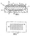
- FIG. 1 represents a power module 1 associated with a water collector 10 in molded plastic having a vein 11 in which circulates water of cooling.
- the power module 1 comprises a sole 3 made of composite AISiC (Aluminum Silicon carbide) sealingly attached to the water collector 10 and comprising a lower face provided with pins 3b, shown in Figure 2, dipping into the fluid stream 11 of the collector 10 and promoting the heat exchange between the soleplate 3 in AISiC and the coolant.
- AISiC Alignment-Betadium Silicon carbide
- the upper face of the sole 3 in AISiC has an alloy skin 4 of aluminum which is coated with a layer of aluminum oxide of a thickness from 50 ⁇ m to 100 ⁇ m providing electrical insulation allowing support differential voltages between the two faces of the oxide layer aluminum over 1000V without breakdown.
- the sole 3 provided with its layer 5 of aluminum oxide, constitutes a substrate on which tracks 6 are metallized in a predetermined pattern to serve as a current collector with three groups of IGBT components 7 brazed on said tracks 6.
- feed tracks 6 of each of the three IGBTs are separated from each other to allow the realization of a three-phase half-inverter on a single substrate.
- the sole 3 in AlSiC is conventionally made by injection of aluminum in a mold on silicon carbide fibers, the shape of the mold being adapted so that the aluminum skin 4 is formed on the upper surface of the sole 3 in AlSiC.
- the lower face of the sole 3 in contact with the coolant may also include a aluminum skin with pimples or microchannels, made directly during the molding operation of the sole 3 by a suitable form of the mold.
- the skin 4 aluminum alloy of the sole 3 is then covered with a layer 5 of aluminum oxide by anodizing the skin 4 in sulfuric acid.
- this anodization makes it possible to obtain an oxide thickness about 20 ⁇ m of aluminum, the thickness of aluminum oxide being limited by the dissolution of the oxide formed in the acid.
- the anodizing will be performed at a temperature of 0 ° C to obtain an oxide thickness aluminum, up to 100 ⁇ m, and the oxide deposit thus obtained will be immersed in hot water to reduce the porosity of the oxide layer 5 of aluminum by formation of aluminum hydroxide.
- the thickness of the layer 5 of aluminum oxide thus formed depends also the aluminum content of the alloy used to constitute the skin 4, because the more the alloy used is rich in aluminum plus the thickness of the oxide layer 5 of aluminum created by anodizing is important.
- the upper face Sa of the aluminum oxide layer 5 is then metallized by electrolytic deposition of copper on tracks 6 previously activated by treatment UV laser then nickel plated by electroless process, the adhesion of the metal layers being reinforced by annealing at 400-500 ° C tolerable by aluminum and its alloys.
- a similar method of metallization is described in patent application FR-A1-2 681 078.
- the IGBT components 7 are then brazed in a conventional manner on the 6 tracks of copper.
- Such a manufacturing process makes it possible to have a very good thermal conduction between the aluminum oxide layer 5 and the skin 4 thanks to the interpenetration of the layer 4 with the skin 4.
- the skin 4 being obtained directly during the molding of the sole 3 in AlSiC, forms a single body with the sole 3, without separation interface, which ensures excellent thermal conductivity between the skin 4 and the sole 3.
- Such a manufacturing method makes it possible to produce a module of inexpensive power ensuring good cooling of power components because of the very good thermal conductivity between the different layers of the power module.
- the substrate thus obtained has very little differences in thermal expansion between the layers and therefore has a very good reliability by presenting very little risk of delamination of solders after a number important thermal cycle.
- Such a manufacturing process also allows to adapt the thickness of the aluminum oxide layer constituting the electrical insulator as needed power module to minimize oxide layer thickness and thus reduce its thermal resistance.
- FIG. 4 presents a second embodiment of the power module according to the invention being different from the first embodiment previously described by the fact that the sole 3 is entirely made of aluminum alloy.
- the power module 1 comprises a sole 3 in aluminum having a lower face, in contact with the cooling fluid, provided with pins 3b obtained directly during the molding of the sole 3 in aluminum.
- the upper face of the sole 3 is covered with a layer 5 of oxide of aluminum obtained by anodization according to a process similar to that described for first embodiment of the invention.
- Tracks are metallized on the layer 5 of aluminum oxide, according to a process similar to that described for the first embodiment, to serve as a current collector for three groups of IGBT 7 components, the latter soldered to the tracks by soldering soft type tin, lead or silver able to accommodate dilations differential.
- Such an embodiment variant of the invention makes it possible to further reduce the cost of manufacture of the power module by removing the use of composite in AlSiC and replacing it with aluminum alloy.
- the module of power thus obtained will have a lower reliability in the thermal cycle of the made of the highest differential expansion between the power components and the aluminum sole and will therefore require the use of soft solder for braze the components.
Landscapes
- Cooling Or The Like Of Semiconductors Or Solid State Devices (AREA)
Description
- la semelle est en composite AlSiC ;
- la semelle est en aluminium ;
- la semelle au contact du fluide de refroidissement comporte des picots ou des microcanaux plongeant à l'intérieur du fluide, les picots ou microcanaux étant réalisés directement dans la semelle ou dans une peau d'aluminium rapportée sur la semelle ;
- les pistes métallisées sont réalisées par dépôt de cuivre ;
- les composants de puissance sont brasés sur les pistes de cuivre ;
- les composants de puissance sont des composants IGBT ;
- trois groupes de composants IGBT sont brasés sur un même substrat, les pistes de chaque groupe d'IGBT étant séparées les unes des autres de telle sorte que deux substrats constituent un onduleur triphasé.
- la couche d'oxyde obtenue est immergée dans de l'eau chaude pour former de l'hydroxyde d'aluminium en surface afin de réduire la porosité de la couche d'oxyde d'aluminium ;
- la peau en alliage d'aluminium recouvrant la semelle est obtenue directement lors du moulage de la semelle par une forme adaptée du moule ;
- la couche d'oxyde d'aluminium est métallisée par dépôt électrolytique de cuivre sur des pistes préalablement activées par traitement au laser Ultraviolet, les pistes de cuivre étant ensuite nickelées par procédé électroless.
- la figure 1 est une vue schématique en coupe d'un module de puissance, selon un premier mode de réalisation de l'invention, monté sur un collecteur d'eau ;
- la figure 2 est une vue de dessous du module de puissance de la figure 1 ;
- la figure 3 est une vue de dessus du module de puissance de la figure 1 ;
- la figure 4 est une vue schématique en coupe d'un module de puissance selon un second mode de réalisation de l'invention.
Claims (12)
- Module de puissance (1) à composants électroniques de puissance (7) comportant une semelle (3) constituant un échangeur de chaleur chargé d'évacuer les dissipations de puissance par effet joule desdits composants de puissance, caractérisé en ce que ladite semelle (3) comporte une face munie d'une peau (4) en alliage d'aluminium, ladite peau (4) étant recouverte d'une couche isolante (5) d'oxyde d'aluminium obtenue par anodisation de ladite peau (4), ladite couche isolante (5) constituant un substrat sur lequel des pistes métallisées (6) sont réalisées afin de recevoir lesdits composants électroniques (7), l'autre face de ladite semelle (3) étant en contact avec un fluide de refroidissement.
- Module de puissance selon la revendication 1, caractérisé en ce que ladite semelle (3) est en composite AlSiC.
- Module de puissance selon la revendication 1, caractérisé en ce que ladite semelle (3) est en aluminium.
- Module de puissance selon l'une quelconque des revendication 1 à 3, caractérisé en ce que la face de la semelle (3) au contact du fluide de refroidissement comporte des picots (3b) ou des microcanaux plongeant à l'intérieur dudit fluide, lesdits picots (3b) ou microcanaux étant réalisés directement dans la semelle (3) ou dans une peau d'aluminium rapportée sur ladite semelle (3).
- Module de puissance selon l'une quelconques des revendications 1 à 4, caractérisé en ce que les pistes métallisées (6) sont réalisées par dépôt de cuivre.
- Module de puissance selon la revendication 5, caractérisé en ce que lesdits composants de puissance (7) sont brasés sur lesdites pistes (6) de cuivre.
- Module de puissance selon l'une quelconque des revendications 1 à 6, caractérisé en ce que lesdits composants de puissance (7) sont des composants IGBT.
- Module de puissance selon la revendication 7, caractérisé en ce que trois groupes de composants IGBT (7) sont brasés sur un même substrat, les pistes (6) de chaque groupe d'IGBT (7) étant séparées les unes des autres de telle sorte que deux substrats constituent un onduleur triphasé.
- Procédé de fabrication d'un module de puissance (1) selon l'une quelconque des revendications 1 à 8, caractérisé en ce que ladite couche (5) d'oxyde d'aluminium est obtenue par anodisation de la peau (4) en alliage d'aluminium dans de l'acide sulfurique au voisinage de 0°C.
- Procédé de fabrication selon la revendication 9, caractérisé en ce que la couche (5) ainsi obtenue est immergée dans de l'eau chaude pour former de l'hydroxyde d'aluminium en surface afin de réduire la porosité de ladite couche (5) d'oxyde d'aluminium.
- Procédé de fabrication selon l'une quelconques des revendications 9 à 10, caractérisé en ce que la peau (4) en alliage d'aluminium recouvrant la semelle (3) est obtenue directement lors du moulage de ladite semelle (3) par une forme adaptée du moule.
- Procédé de fabrication selon l'une quelconque des revendications 9 à 11, caractérisé en ce que la couche (5) d'oxyde d'aluminium est métallisée par dépôt électrolytique de cuivre sur des pistes (6) préalablement activées par traitement au laser Ultraviolet, lesdites pistes de cuivre (6) étant ensuite nickelées par procédé électroless.
Applications Claiming Priority (2)
| Application Number | Priority Date | Filing Date | Title |
|---|---|---|---|
| FR0008121 | 2000-06-23 | ||
| FR0008121A FR2810845B1 (fr) | 2000-06-23 | 2000-06-23 | Module de puissance a composants electroniques de puissance et procede de fabrication d'un tel module |
Publications (2)
| Publication Number | Publication Date |
|---|---|
| EP1168906A1 EP1168906A1 (fr) | 2002-01-02 |
| EP1168906B1 true EP1168906B1 (fr) | 2005-09-14 |
Family
ID=8851642
Family Applications (1)
| Application Number | Title | Priority Date | Filing Date |
|---|---|---|---|
| EP01401458A Expired - Lifetime EP1168906B1 (fr) | 2000-06-23 | 2001-06-06 | Module de puissance à composants électroniques de puissance et procédé de fabrication d'un tel module |
Country Status (6)
| Country | Link |
|---|---|
| US (1) | US20020001177A1 (fr) |
| EP (1) | EP1168906B1 (fr) |
| CA (1) | CA2351106A1 (fr) |
| DE (1) | DE60113337T2 (fr) |
| ES (1) | ES2248251T3 (fr) |
| FR (1) | FR2810845B1 (fr) |
Families Citing this family (17)
| Publication number | Priority date | Publication date | Assignee | Title |
|---|---|---|---|---|
| DE20115922U1 (de) * | 2001-01-11 | 2002-01-17 | Siemens AG, 80333 München | Kunststoff-Schaltplatte eines hydraulischen Kraftfahrzeug-Getriebesteuergerätes |
| DE102004018475A1 (de) * | 2004-04-16 | 2005-11-10 | eupec Europäische Gesellschaft für Leistungshalbleiter mbH | Leistungshalbleiteranordnung |
| JP2006100770A (ja) * | 2004-09-01 | 2006-04-13 | Toyota Industries Corp | 回路基板のベース板の製造方法及び回路基板のベース板並びにベース板を用いた回路基板 |
| KR100764388B1 (ko) * | 2006-03-17 | 2007-10-05 | 삼성전기주식회사 | 양극산화 금속기판 모듈 |
| KR100764386B1 (ko) * | 2006-03-20 | 2007-10-08 | 삼성전기주식회사 | 고온공정에 적합한 절연구조체 및 그 제조방법 |
| JP4315187B2 (ja) * | 2006-11-20 | 2009-08-19 | カシオ計算機株式会社 | 携帯電子機器 |
| DE102008035485A1 (de) * | 2008-07-30 | 2010-02-04 | Brose Fahrzeugteile GmbH & Co. Kommanditgesellschaft, Würzburg | Vorrichtung, insbesondere zur Stromleitung, um ein Verfahren zur Herstellung einer Vorrichtung, insbesondere zur Stromleitung |
| DK2456908T3 (en) * | 2009-07-23 | 2016-10-10 | Carrier Corp | A method of forming an oxide layer brazed ON AN ARTICLE |
| EP2328172B1 (fr) * | 2009-10-02 | 2019-06-26 | Abb Research Ltd. | Agencement électronique de puissance |
| DE102010000082B4 (de) * | 2010-01-14 | 2012-10-11 | Woodward Kempen Gmbh | Schaltungsanordnung von elektronischen Leistungsschaltern einer Stromerzeugungsvorrichtung |
| DE102010001565A1 (de) * | 2010-02-04 | 2011-08-04 | Robert Bosch GmbH, 70469 | Leistungsmodul mit einer Schaltungsanordnung, elektrische/elektronische Schaltungsanordnung, Verfahren zur Herstellung eines Leistungsmoduls |
| US8203839B2 (en) * | 2010-03-10 | 2012-06-19 | Toyota Motor Engineering & Manufacturing North America, Inc. | Cooling devices, power modules, and vehicles incorporating the same |
| US9312200B1 (en) * | 2013-03-13 | 2016-04-12 | Amazon Technologies, Inc. | Solid structures for thermal management |
| DE102014105000B4 (de) * | 2014-04-08 | 2021-02-25 | Infineon Technologies Ag | Verfahren zur Herstellung und zum Bestücken eines Schaltungsträgers |
| DE102016125348B4 (de) | 2016-12-22 | 2020-06-25 | Rogers Germany Gmbh | Trägersubstrat für elektrische Bauteile und Verfahren zur Herstellung eines Trägersubstrats |
| DE102019129675A1 (de) | 2018-12-11 | 2020-06-18 | Infineon Technologies Ag | Leistungshalbleitermodul und Verfahren zum Herstellen eines Leistungshalbleitermoduls |
| CN114334872B (zh) * | 2022-03-15 | 2022-06-14 | 合肥阿基米德电子科技有限公司 | 具有散热结构的电力电子器件igbt模块及制备方法 |
Family Cites Families (4)
| Publication number | Priority date | Publication date | Assignee | Title |
|---|---|---|---|---|
| DE3147789A1 (de) * | 1981-12-03 | 1983-06-09 | Brown, Boveri & Cie Ag, 6800 Mannheim | Leistungsmodul und verfahren zu seiner herstellung |
| EP0471552B1 (fr) * | 1990-08-14 | 1997-07-02 | Texas Instruments Incorporated | Module de transport de chaleur pour des applications à très haute densité et à empaquetage silicium sur silicium |
| JP3164518B2 (ja) * | 1995-12-21 | 2001-05-08 | 古河電気工業株式会社 | 平面型ヒートパイプ |
| FR2747005B1 (fr) * | 1996-03-26 | 1998-06-19 | Thomson Csf | Boitier de micro-electronique avec systeme de refroidissement |
-
2000
- 2000-06-23 FR FR0008121A patent/FR2810845B1/fr not_active Expired - Fee Related
-
2001
- 2001-06-06 DE DE60113337T patent/DE60113337T2/de not_active Expired - Fee Related
- 2001-06-06 ES ES01401458T patent/ES2248251T3/es not_active Expired - Lifetime
- 2001-06-06 EP EP01401458A patent/EP1168906B1/fr not_active Expired - Lifetime
- 2001-06-13 US US09/879,130 patent/US20020001177A1/en not_active Abandoned
- 2001-06-18 CA CA002351106A patent/CA2351106A1/fr not_active Abandoned
Also Published As
| Publication number | Publication date |
|---|---|
| EP1168906A1 (fr) | 2002-01-02 |
| DE60113337D1 (de) | 2005-10-20 |
| CA2351106A1 (fr) | 2001-12-23 |
| FR2810845B1 (fr) | 2002-08-23 |
| ES2248251T3 (es) | 2006-03-16 |
| DE60113337T2 (de) | 2006-06-22 |
| FR2810845A1 (fr) | 2001-12-28 |
| US20020001177A1 (en) | 2002-01-03 |
Similar Documents
| Publication | Publication Date | Title |
|---|---|---|
| EP1168906B1 (fr) | Module de puissance à composants électroniques de puissance et procédé de fabrication d'un tel module | |
| FR2813440A1 (fr) | Dispositif a semiconducteur pour la commande d'energie electrique | |
| EP1005083B1 (fr) | Composant électronique de puissance comportant des moyens de refroidissement | |
| FR2906645A1 (fr) | Module de semiconducteur de puissance | |
| FR2829874A1 (fr) | Systeme a semi-conducteur a boitier et enveloppe | |
| WO2018189468A1 (fr) | Module électronique de puissance et convertisseur électrique de puissance l'incorporant | |
| FR2625602A1 (fr) | Procede de fabrication de condensateurs electrolytiques a l'aluminium et condensateur a anode integree obtenu par ce procede | |
| CA2352513A1 (fr) | Procede de fabrication d'un composant electronique de puissance, et composant electronique de puissance ainsi obtenu | |
| EP1189277A1 (fr) | Substrat pour circuit électronique et module électronique utilisant un tel substrat | |
| EP1239515B1 (fr) | Substrat pour circuit électronique de puissance et module électronique de puissance utilisant un tel substrat | |
| FR2514565A1 (fr) | Ensemble a pile solaire et procede de fixation d'une barre omnibus a une pile solaire | |
| EP0395544B1 (fr) | Substrats métalliques isolés et procédé de fabrication desdits substrats | |
| FR3094565A1 (fr) | Refroidissement de dispositifs électroniques | |
| FR2659494A1 (fr) | Composant semiconducteur de puissance, dont la puce est montee a l'envers. | |
| EP0734066B1 (fr) | Module électronique de puissance | |
| EP0793269B1 (fr) | Dispositif semiconducteur incluant une puce munie d'une ouverture de via et soudée sur un support, et procédé de réalisation de ce dispositif | |
| EP1417711B1 (fr) | Module de composants electroniques de puissance et procede d'assemblage d'un tel module | |
| EP0997940B1 (fr) | Procédé de raccordement électrique de puces de transistor IGBT montées sur une plaquette de circuits intégrés | |
| FR2822591A1 (fr) | Assemblage de composants d'epaisseurs diverses | |
| FR2786658A1 (fr) | Structure composite pour composant electronique de puissance procede de fabrication de cette structure et composant electronique de puissance pourvu d'une telle structure | |
| FR2814280A1 (fr) | Substrat pour circuit electronique de puissance et module electronique de puissance utilisant un tel substrat | |
| EP4062447B1 (fr) | Cadre metallique conducteur pour module électronique de puissance et procede de fabrication associe | |
| JP2003046047A (ja) | 電子パワー素子を有するパワーモジュール及びそのようなモジュールの製造方法 | |
| JP3520161B2 (ja) | 半導体装置,及びその製造方法 | |
| FR3144399A1 (fr) | Module électronique de puissance multi-étages |
Legal Events
| Date | Code | Title | Description |
|---|---|---|---|
| PUAI | Public reference made under article 153(3) epc to a published international application that has entered the european phase |
Free format text: ORIGINAL CODE: 0009012 |
|
| AK | Designated contracting states |
Kind code of ref document: A1 Designated state(s): AT BE CH CY DE DK ES FI FR GB GR IE IT LI LU MC NL PT SE TR Kind code of ref document: A1 Designated state(s): CH DE ES GB IT LI SE |
|
| AX | Request for extension of the european patent |
Free format text: AL;LT;LV;MK;RO;SI |
|
| 17P | Request for examination filed |
Effective date: 20020702 |
|
| AKX | Designation fees paid |
Free format text: CH DE ES GB IT LI SE |
|
| RAP1 | Party data changed (applicant data changed or rights of an application transferred) |
Owner name: ALSTOM |
|
| GRAP | Despatch of communication of intention to grant a patent |
Free format text: ORIGINAL CODE: EPIDOSNIGR1 |
|
| RTI1 | Title (correction) |
Free format text: POWER MODULE WITH ELECTRONIC POWER COMPONENTS AND PRODUCTION METHOD THEREOF |
|
| GRAS | Grant fee paid |
Free format text: ORIGINAL CODE: EPIDOSNIGR3 |
|
| GRAA | (expected) grant |
Free format text: ORIGINAL CODE: 0009210 |
|
| AK | Designated contracting states |
Kind code of ref document: B1 Designated state(s): CH DE ES GB IT LI SE |
|
| REG | Reference to a national code |
Ref country code: GB Ref legal event code: FG4D Free format text: NOT ENGLISH |
|
| REG | Reference to a national code |
Ref country code: CH Ref legal event code: EP |
|
| REF | Corresponds to: |
Ref document number: 60113337 Country of ref document: DE Date of ref document: 20051020 Kind code of ref document: P |
|
| REG | Reference to a national code |
Ref country code: SE Ref legal event code: TRGR |
|
| GBT | Gb: translation of ep patent filed (gb section 77(6)(a)/1977) |
Effective date: 20051212 |
|
| REG | Reference to a national code |
Ref country code: ES Ref legal event code: FG2A Ref document number: 2248251 Country of ref document: ES Kind code of ref document: T3 |
|
| PLBE | No opposition filed within time limit |
Free format text: ORIGINAL CODE: 0009261 |
|
| STAA | Information on the status of an ep patent application or granted ep patent |
Free format text: STATUS: NO OPPOSITION FILED WITHIN TIME LIMIT |
|
| 26N | No opposition filed |
Effective date: 20060615 |
|
| PGFP | Annual fee paid to national office [announced via postgrant information from national office to epo] |
Ref country code: SE Payment date: 20070614 Year of fee payment: 7 |
|
| PGFP | Annual fee paid to national office [announced via postgrant information from national office to epo] |
Ref country code: CH Payment date: 20070615 Year of fee payment: 7 |
|
| PGFP | Annual fee paid to national office [announced via postgrant information from national office to epo] |
Ref country code: DE Payment date: 20070622 Year of fee payment: 7 |
|
| PGFP | Annual fee paid to national office [announced via postgrant information from national office to epo] |
Ref country code: ES Payment date: 20070628 Year of fee payment: 7 |
|
| PGFP | Annual fee paid to national office [announced via postgrant information from national office to epo] |
Ref country code: GB Payment date: 20070621 Year of fee payment: 7 |
|
| PGFP | Annual fee paid to national office [announced via postgrant information from national office to epo] |
Ref country code: IT Payment date: 20070623 Year of fee payment: 7 |
|
| REG | Reference to a national code |
Ref country code: CH Ref legal event code: PL |
|
| EUG | Se: european patent has lapsed | ||
| GBPC | Gb: european patent ceased through non-payment of renewal fee |
Effective date: 20080606 |
|
| PG25 | Lapsed in a contracting state [announced via postgrant information from national office to epo] |
Ref country code: DE Free format text: LAPSE BECAUSE OF NON-PAYMENT OF DUE FEES Effective date: 20090101 |
|
| PG25 | Lapsed in a contracting state [announced via postgrant information from national office to epo] |
Ref country code: GB Free format text: LAPSE BECAUSE OF NON-PAYMENT OF DUE FEES Effective date: 20080606 Ref country code: LI Free format text: LAPSE BECAUSE OF NON-PAYMENT OF DUE FEES Effective date: 20080630 Ref country code: CH Free format text: LAPSE BECAUSE OF NON-PAYMENT OF DUE FEES Effective date: 20080630 |
|
| REG | Reference to a national code |
Ref country code: ES Ref legal event code: FD2A Effective date: 20080607 |
|
| PG25 | Lapsed in a contracting state [announced via postgrant information from national office to epo] |
Ref country code: IT Free format text: LAPSE BECAUSE OF NON-PAYMENT OF DUE FEES Effective date: 20080606 |
|
| PG25 | Lapsed in a contracting state [announced via postgrant information from national office to epo] |
Ref country code: ES Free format text: LAPSE BECAUSE OF NON-PAYMENT OF DUE FEES Effective date: 20080607 |
|
| PG25 | Lapsed in a contracting state [announced via postgrant information from national office to epo] |
Ref country code: SE Free format text: LAPSE BECAUSE OF NON-PAYMENT OF DUE FEES Effective date: 20080607 |