EP1176476A2 - Rouleau conducteur et procédé de sa production - Google Patents
Rouleau conducteur et procédé de sa production Download PDFInfo
- Publication number
- EP1176476A2 EP1176476A2 EP01118140A EP01118140A EP1176476A2 EP 1176476 A2 EP1176476 A2 EP 1176476A2 EP 01118140 A EP01118140 A EP 01118140A EP 01118140 A EP01118140 A EP 01118140A EP 1176476 A2 EP1176476 A2 EP 1176476A2
- Authority
- EP
- European Patent Office
- Prior art keywords
- roll
- conductive
- resistance value
- conductive roll
- layer
- Prior art date
- Legal status (The legal status is an assumption and is not a legal conclusion. Google has not performed a legal analysis and makes no representation as to the accuracy of the status listed.)
- Withdrawn
Links
Images
Classifications
-
- G—PHYSICS
- G03—PHOTOGRAPHY; CINEMATOGRAPHY; ANALOGOUS TECHNIQUES USING WAVES OTHER THAN OPTICAL WAVES; ELECTROGRAPHY; HOLOGRAPHY
- G03G—ELECTROGRAPHY; ELECTROPHOTOGRAPHY; MAGNETOGRAPHY
- G03G15/00—Apparatus for electrographic processes using a charge pattern
- G03G15/02—Apparatus for electrographic processes using a charge pattern for laying down a uniform charge, e.g. for sensitising; Corona discharge devices
- G03G15/0208—Apparatus for electrographic processes using a charge pattern for laying down a uniform charge, e.g. for sensitising; Corona discharge devices by contact, friction or induction, e.g. liquid charging apparatus
- G03G15/0216—Apparatus for electrographic processes using a charge pattern for laying down a uniform charge, e.g. for sensitising; Corona discharge devices by contact, friction or induction, e.g. liquid charging apparatus by bringing a charging member into contact with the member to be charged, e.g. roller, brush chargers
- G03G15/0233—Structure, details of the charging member, e.g. chemical composition, surface properties
-
- G—PHYSICS
- G03—PHOTOGRAPHY; CINEMATOGRAPHY; ANALOGOUS TECHNIQUES USING WAVES OTHER THAN OPTICAL WAVES; ELECTROGRAPHY; HOLOGRAPHY
- G03G—ELECTROGRAPHY; ELECTROPHOTOGRAPHY; MAGNETOGRAPHY
- G03G15/00—Apparatus for electrographic processes using a charge pattern
- G03G15/06—Apparatus for electrographic processes using a charge pattern for developing
- G03G15/08—Apparatus for electrographic processes using a charge pattern for developing using a solid developer, e.g. powder developer
- G03G15/0806—Apparatus for electrographic processes using a charge pattern for developing using a solid developer, e.g. powder developer on a donor element, e.g. belt, roller
- G03G15/0818—Apparatus for electrographic processes using a charge pattern for developing using a solid developer, e.g. powder developer on a donor element, e.g. belt, roller characterised by the structure of the donor member, e.g. surface properties
-
- G—PHYSICS
- G03—PHOTOGRAPHY; CINEMATOGRAPHY; ANALOGOUS TECHNIQUES USING WAVES OTHER THAN OPTICAL WAVES; ELECTROGRAPHY; HOLOGRAPHY
- G03G—ELECTROGRAPHY; ELECTROPHOTOGRAPHY; MAGNETOGRAPHY
- G03G15/00—Apparatus for electrographic processes using a charge pattern
- G03G15/14—Apparatus for electrographic processes using a charge pattern for transferring a pattern to a second base
- G03G15/16—Apparatus for electrographic processes using a charge pattern for transferring a pattern to a second base of a toner pattern, e.g. a powder pattern, e.g. magnetic transfer
- G03G15/1665—Apparatus for electrographic processes using a charge pattern for transferring a pattern to a second base of a toner pattern, e.g. a powder pattern, e.g. magnetic transfer by introducing the second base in the nip formed by the recording member and at least one transfer member, e.g. in combination with bias or heat
- G03G15/167—Apparatus for electrographic processes using a charge pattern for transferring a pattern to a second base of a toner pattern, e.g. a powder pattern, e.g. magnetic transfer by introducing the second base in the nip formed by the recording member and at least one transfer member, e.g. in combination with bias or heat at least one of the recording member or the transfer member being rotatable during the transfer
- G03G15/1685—Structure, details of the transfer member, e.g. chemical composition
-
- G—PHYSICS
- G03—PHOTOGRAPHY; CINEMATOGRAPHY; ANALOGOUS TECHNIQUES USING WAVES OTHER THAN OPTICAL WAVES; ELECTROGRAPHY; HOLOGRAPHY
- G03G—ELECTROGRAPHY; ELECTROPHOTOGRAPHY; MAGNETOGRAPHY
- G03G2215/00—Apparatus for electrophotographic processes
- G03G2215/08—Details of powder developing device not concerning the development directly
- G03G2215/0855—Materials and manufacturing of the developing device
- G03G2215/0858—Donor member
- G03G2215/0863—Manufacturing
-
- Y—GENERAL TAGGING OF NEW TECHNOLOGICAL DEVELOPMENTS; GENERAL TAGGING OF CROSS-SECTIONAL TECHNOLOGIES SPANNING OVER SEVERAL SECTIONS OF THE IPC; TECHNICAL SUBJECTS COVERED BY FORMER USPC CROSS-REFERENCE ART COLLECTIONS [XRACs] AND DIGESTS
- Y10—TECHNICAL SUBJECTS COVERED BY FORMER USPC
- Y10T—TECHNICAL SUBJECTS COVERED BY FORMER US CLASSIFICATION
- Y10T29/00—Metal working
- Y10T29/49—Method of mechanical manufacture
- Y10T29/49544—Roller making
- Y10T29/49547—Assembling preformed components
- Y10T29/49549—Work contacting surface element assembled to core
Definitions
- the present invention relates to a conductive roll used in an electrophotographic apparatus such as a copying machine or a printer using electrophotography, particularly a charging roll, a developing roll or a transfer roll used around a photosensitive drum of such an apparatus.
- an electrophotographic apparatus such as a copying machine or a printer using electrophotography
- conductive rolls such as a charging roll, a developing roll and a transfer roll around a photosensitive drum for forming an electrostatic latent image.
- These conductive rolls have a basic structure in which an elastic conductive layer made of a low-hardness rubber elastic material or a rubber foamed material is provided on an outer periphery of a conductive metal shaft (core), and an intermediate layer and a surface layer for adjustment of resistance are sequentially laminated as required on the outer periphery thereof.
- a conductive roll having such a structure has prescribed electric characteristics (resistance value and electrostatic capacity) to transmit a voltage impressed on the core to a photosensitive drum.
- the charging roll in order for the charging roll to control charging ability of the photosensitive drum, for the developing roll to control toner charging property and transferability of toner (developing agent) to the photosensitive drum, and for the transfer roll to control transferability of toner to a sheet or to an OHP film, these rolls must have respective prescribed resistance values, and at the same time, it is necessary to achieve a uniform resistance value throughout each roll.
- Efforts are made to achieve a uniform target resistance value for these conductive rolls through studies of material properties and structural design. That is, when adding conductive particles (carbon black, in general) which govern the resistance value to layers of the roll, the type, quantity of addition and dispersibility of these particles are controlled so as to achieve a uniform resistance of roll. Use of an ion conductive agent having greater dispersibility than carbon black is being tried. In terms of structural design, efforts are made to achieve a uniform resistance value by using a roll structure comprising a plurality of layers in lamination, and combining resistance values of the individual layers in the lamination in various manners.
- conductive particles carbon black, in general
- the controlled range of the resistance values of conductive rolls varies with the location of the charging roll, the developing roll or the transfer roll, the service conditions and the like.
- the allowable range for uniformity of resistance value is believed to be such that the difference in the logarithmically converted value between maximum and minimum measured resistance values of the roll, as expressed in the number of digits, should be within 0.3 digits.
- the aforementioned conductive rolls such as charging roll, a developing roll or a transfer roll, when used in combination with a photosensitive drum, inevitably come into contact with toner (developing agent).
- toner developer
- various additives for controlling charging characteristics, strippability and fixability are added to the interior or exterior of the developing agent, a so-called filming phenomenon tends to be easily caused, in which these interior and exterior additives and a polymer itself of the developing agent are deposited onto the roll surface.
- applicable interior and exterior additives to the developing agent generally include, in addition to commonly used silica, metal oxides such as aluminum oxide and titanium oxide, metals salts such as calcium sulfate and calcium carbonate, and fatty acid salts such as zinc stearate. Since these substances have a high insulation or a high resistance because of their purpose of use, the roll resistance value increases accordingly as the quantity of deposition onto the roll surface increases. While this increase in resistance value can be compensated through adjustment of the voltage impressed onto the roll, there are blurs in deposition onto the roll surface caused by the filming phenomenon, leading to a non-uniform resistance value for the roll as a whole.
- This filming phenomenon is considered to be caused by strippability of the material itself forming the roll surface, forming conditions such as distribution of vulcanizing temperature, or a surface condition of the roll.
- efforts have conventionally been made to develop a new material and a manufacturing process.
- the developing agent being used has tended to have a lower melting point and a smaller diameter, and thus the agent is becoming easier to adhere to the roll.
- deposit blurs tend to become larger, and the resultant image is more susceptible to uneven density.
- the present invention has an object to provide a conductive roll for an electrophotographic apparatus and a manufacturing method thereof which eliminates deposition blurs caused by the filming phenomenon on the surface of a conductive roll such as a charging roll, a developing roll or a transfer roll, inhibits non-uniform roll resistance values, and gives a satisfactory image free from density blurs.
- the present invention therefore provides a conductive roll for an electrophotographic apparatus, having at least an elastic conductive layer provided on an outer periphery of a metal shaft thereof; wherein the roll surface thereof is corona-treated.
- the manufacturing method of a conductive roll of the invention comprises the steps of arranging the conductive roll oppositely to, and in parallel with, an electrode for discharging, and corona-treating the surface of the conductive roll by impressing a voltage onto the electrode while rotating the conductive roll.
- the corona treatment used in the present invention is a local discharge phenomenon caused by partial insulation breakage occurring upon emergence of strong unequal electric fields around a conductor, and has conventionally been applied generally for the purpose of improving depositability of a resin material.
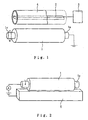
- corona discharge is produced in a conductive roll 1 by arranging a discharging electrode 2 comprising aluminum or the like in parallel with the conductor roll 1 having a grounded shaft 1a (core), for example as shown in Fig. 1, and impressing a prescribed voltage from a power source 3 onto the electrode 2 while rotating the conductor roll 1 at a constant speed.
- a discharging electrode 2 comprising aluminum or the like in parallel with the conductor roll 1 having a grounded shaft 1a (core), for example as shown in Fig. 1, and impressing a prescribed voltage from a power source 3 onto the electrode 2 while rotating the conductor roll 1 at a constant speed.
- an insulator such as a glass tube 4 preferably should be placed between the conductive roll 1 and the electrode 2.
- Preferred corona treatment conditions used in the invention include a distance between the conductive roll and the electrode arranged in parallel with each other within a range of from 0.5 to 5.0 mm, a voltage impressed onto the electrode within a range of from 0.1 to 1.0 kW, and a treatment time within a range of from 1 to 600 seconds.
- a distance between the conductive roll and the electrode of less than 0.5 mm a short-circuit leakage may be caused by discharge, and the roll surface may be broken.
- a distance of more than 5.0 mm in contrast, even application of a higher voltage may not cause corona discharge.
- a voltage impressed onto the electrode of under 0.1 kW corona discharge may not occur, and with a voltage of over 1.0 kW, a short-circuit leakage may be caused by discharge, resulting in breakage of the roll surface.
- the conductive roll corona-treated according to the invention if applied as a charging roll, a developing roll or a transfer roll, can retain stable properties and can give an excellent image which is free from density blurs for a long period of time.
- the roll resistance continued value gradually increases.
- the corona treatment being a reforming treatment, does not impair the basic properties of the material composing the roll. Therefore, when dispersing conductive particles such as carbon black particles for controlling electrical characteristics, or setting material properties of the roll such as wear resistance, no restriction is imposed, permitting free design as to the basic configuration of the roll.
- Examples of the conductive roll of the invention include a charging roll, a developing roll, and a transfer roll used in an electrophotographic apparatus such as a copying machine or a printer.
- the structure of the conductive roll is such that at least an elastic conductive layer is provided on an outer periphery of a metal shaft (core).
- the roll may be one having, for example, a single or multiple rubber layer(s) and/or resin layer(s) on an outer periphery of the elastic conductive layer.
- These elastic conductive layers may be solid or sponge-like.
- the materials of the elastic conductive layer and a single or multiple rubber layer(s) or resin layer(s) provided on the outer periphery thereof.
- a material capable of being formed into a roll can generally be adopted. More specifically, applicable rubber materials include urethane rubber, nitrile butadiene rubber (NBR), styrene-butadiene rubber (SBR), ethylene-propylenediene terpolymer (EPDM), chloroprene rubber (CR), silicone rubber, fluororubber, hydrin rubber, isoprene rubber (IR), and butadiene rubber (BR).
- NBR nitrile butadiene rubber
- SBR styrene-butadiene rubber
- EPDM ethylene-propylenediene terpolymer
- CR chloroprene rubber
- silicone rubber silicone rubber
- fluororubber fluororubber
- IR isoprene rubber
- BR butadiene rubber
- Applicable resin materials include urethane resin, acrylic resin, nylon resin (polyamide resin), polycarbonate resin, polyvinyl chloride (PVC), polypropylene (PP), and fluororesin.
- the corona treatment of the invention is particularly effective for silicone rubber, hydrogenated nitrile butadiene rubber (H-NBR) and fluororesin which usually tend to suffer from very non-uniform deposition.
- the method of forming the conductive roll comprises the steps of arranging a metal shaft (core), previously subjected as required to nickel plating on the surface or coated with an adhesive, in a mold divided into an upper portion and a lower portion; filling the cavity between the shaft and the mold with any of the above-mentioned rubber materials or resin materials; and heating and pressurizing the same for a necessary period of time, thereby forming a roll (elastic conductive layer).
- the rubber materials or the resin materials may be in a molten state, in a solution state dissolved into an organic solvent, or a compound, and may be in any form.
- the outer periphery of the roll formed as described above is finished into a necessary cylindrical shape by a technique such as cylindrical polishing or the like.
- a layer for resistance adjustment or protection is necessary on the outer periphery of the roll (the elastic conductive layer)
- a prescribed rubber material or resin material is coated by a dipping process or the like and then heated, thereby forming a single or multiple rubber or resin layer(s).
- Conductive roll samples 1 to 4 were manufactured as follows. An electroless Ni plating having a thickness of 4 ⁇ m was applied onto the surface of a shaft (core) made of SUM 22 having an outside diameter of 8 mm, and an elastic conductive layer made of NBR having a thickness of 6 mm was formed by mold forming on the outer periphery of the shaft. The resultant structure was cylindrically polished into roll sample 1. In place of the elastic conductive layer comprising NBR of the above-mentioned roll sample 1, an elastic conductive layer made of SBR having a thickness of 6 mm was formed by mold forming into a roll; a surface layer made of nylon resin having a thickness of 10 ⁇ m was coated thereon; and the same was cylindrically polished into roll sample 2.
- Roll sample 3 was prepared in the same manner as in roll sample 2, except that the elastic conductive layer comprised of silicone rubber having a thickness of 6 mm, with a plurality of surface layers comprising an intermediate layer made of H-NBR having a thickness of 10 ⁇ m and an outermost layer made of fluororubber having a thickness of 10 ⁇ m.
- Roll sample 4 was prepared in the same manner as in roll sample 2, except that roll sample 4 had a surface layer comprising an inner layer made of nylon resin having a thickness of 10 ⁇ m, an intermediate layer made of NBR having a thickness of 100 ⁇ m, and an outermost layer made of nylon resin having a thickness of 10 ⁇ m.
- the conductive rolls of samples 1 to 4 were corona-treated by using a conventional corona discharge unit. More specifically, as shown in Fig. 1, a conductive roll 1 is arranged below an aluminum electrode 2 covered with a glass tube 4 on the exterior, with the roll surface in parallel with the electrode 2 and with a gap of 2 mm in between. A voltage of an output of 0.2 kW was impressed onto the electrode 2 while rotating the conductive roll 1 at 20 rpm and earthing the shaft 1a of the conductive roll 1. Corona discharge was conducted for a period of 60 seconds.
- the roll resistance value was measured, and uniformity of resistance values in the rolls was evaluated.
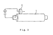
- the results are shown in the following Table 2. More specifically, the roll resistance value was determined by placing the conductive roll 1 on a metal flat plate 5, as shown in Fig. 2, impressing a voltage of DC 100 V between the shaft 1a and the metal plate 5 while the conductive roll 1 is pressed against the metal plate 5 by applying a load of 500 gf at both ends of the shaft 1a, and measuring the quantity of current flowing between the shaft 1a and the metal plate 5.
- a resistance value throughout the entire surface of each roll was determined by pressing a metal roller 6 (bearing) having a width of 12 mm against the outer periphery of the conductive roll 1 with a load of 100 gf, impressing a voltage of DC 100 V between the metal roller 6 and the shaft 1a of the conductive roll 1 while moving the metal roller 6 in the axial direction as the conductive roll 1 is rotated, and measuring the quantity of current flowing between the shaft 1a and the metal roller 6.
- the resistance values were thus measured for the entire surface of the conductive roll.
- the thus determined maximum resistance value Rmax and minimum resistance value Rmin were logarithmically converted, and the determined difference between them (log Rmax/Rmin) was expressed in the forms of number of digits.
- a durability test was carried out by assembling each of the conductive rolls of samples 1-4 of the invention as a transfer roll of a laser beam printer, continuously driving the same under conditions including a temperature of 30°C and a humidity of 85%, and actually printing an image on 10,000 sheets.
- measurement of the roll resistance value and evaluation of uniformity of resistance value within a roll were conducted in the same manner as described above, and deposition onto the roll surface was observed. The results are shown in the following Table 2.
- deposition criteria for the evaluation of deposition included “no deposition” for a state free from deposition or the slightest deposition, “uneven deposition” showing presence of deposition but differences in the quantity of deposition between difference portions, and “uniform deposition” expressing a state in which uniform deposition over the entire surface.
- the present invention depositions uniformly adhere to the roll surface as a result of filming phenomenon by applying a simple method known as corona treatment, thus resulting in uniform deposition free from unevenness. It is thus possible to eliminate unevenness of resistance value within a conductive roll. Therefore, by using the conductive roll of the present invention as a charging roll, a developing roll or a transfer roll in an electrophotographic apparatus, an image free from density unevenness can be stably obtained for a long period of time.
- the corona treatment used in the present invention is a reforming treatment of a roll surface, and does not impair the basic properties of the material composing the conductive roll.
- dispersing charging particles such as carbon black particles or properties of a roll material, therefore, freedom in design is permitted regarding the basic roll configuration, such is not subjected to any restriction.
Landscapes
- Physics & Mathematics (AREA)
- General Physics & Mathematics (AREA)
- Engineering & Computer Science (AREA)
- Plasma & Fusion (AREA)
- Electrostatic Charge, Transfer And Separation In Electrography (AREA)
- Rolls And Other Rotary Bodies (AREA)
- Casting Or Compression Moulding Of Plastics Or The Like (AREA)
- Dry Development In Electrophotography (AREA)
Applications Claiming Priority (2)
| Application Number | Priority Date | Filing Date | Title |
|---|---|---|---|
| JP2000228589A JP3760735B2 (ja) | 2000-07-28 | 2000-07-28 | 導電性ロール |
| JP2000228589 | 2000-07-28 |
Publications (1)
| Publication Number | Publication Date |
|---|---|
| EP1176476A2 true EP1176476A2 (fr) | 2002-01-30 |
Family
ID=18721841
Family Applications (1)
| Application Number | Title | Priority Date | Filing Date |
|---|---|---|---|
| EP01118140A Withdrawn EP1176476A2 (fr) | 2000-07-28 | 2001-07-26 | Rouleau conducteur et procédé de sa production |
Country Status (3)
| Country | Link |
|---|---|
| US (1) | US20020035020A1 (fr) |
| EP (1) | EP1176476A2 (fr) |
| JP (1) | JP3760735B2 (fr) |
Cited By (1)
| Publication number | Priority date | Publication date | Assignee | Title |
|---|---|---|---|---|
| EP2518569A4 (fr) * | 2009-12-21 | 2018-01-10 | Canon Kabushiki Kaisha | Procédé de fabrication de rouleau pour électrophotographie |
Families Citing this family (5)
| Publication number | Priority date | Publication date | Assignee | Title |
|---|---|---|---|---|
| WO2006001171A1 (fr) * | 2004-06-09 | 2006-01-05 | Bridgestone Corporation | Rouleau de developpement, rouleau electrostatique, rouleau conducteur et leur procede de fabrication |
| JP2007298775A (ja) | 2006-04-28 | 2007-11-15 | Sharp Corp | 画像形成装置、帯電ローラ、帯電ローラの製造方法、帯電ローラの製造装置 |
| JP4653204B2 (ja) * | 2008-09-16 | 2011-03-16 | 住友ゴム工業株式会社 | 導電性ロール |
| JP5730112B2 (ja) * | 2011-04-20 | 2015-06-03 | キヤノン株式会社 | 電子写真用ローラの製造方法 |
| JP7621044B2 (ja) * | 2021-09-28 | 2025-01-24 | 住友理工株式会社 | 電子写真機器用帯電ロールおよび電子写真機器用帯電ロールの製造方法 |
-
2000
- 2000-07-28 JP JP2000228589A patent/JP3760735B2/ja not_active Expired - Lifetime
-
2001
- 2001-07-26 EP EP01118140A patent/EP1176476A2/fr not_active Withdrawn
- 2001-07-27 US US09/915,356 patent/US20020035020A1/en not_active Abandoned
Cited By (1)
| Publication number | Priority date | Publication date | Assignee | Title |
|---|---|---|---|---|
| EP2518569A4 (fr) * | 2009-12-21 | 2018-01-10 | Canon Kabushiki Kaisha | Procédé de fabrication de rouleau pour électrophotographie |
Also Published As
| Publication number | Publication date |
|---|---|
| JP2002040759A (ja) | 2002-02-06 |
| US20020035020A1 (en) | 2002-03-21 |
| JP3760735B2 (ja) | 2006-03-29 |
Similar Documents
| Publication | Publication Date | Title |
|---|---|---|
| EP1176476A2 (fr) | Rouleau conducteur et procédé de sa production | |
| US6175712B1 (en) | Intermediate transfer member and image formation apparatus using same | |
| KR0171166B1 (ko) | 대전 부재, 대전 부재 제조 프로세스 및 대전 부재를 갖고 있는 프로세스 카트리지 | |
| US11042107B2 (en) | Intermediate transfer medium and image forming apparatus | |
| US11474444B2 (en) | Intermediate transfer belt and image forming apparatus | |
| US6801741B2 (en) | Image forming apparatus with intermediary transfer member | |
| EP0716354B1 (fr) | Méthode de reconditionnement d'un rouleau de chargement | |
| JP4001123B2 (ja) | 導電性ロール | |
| JP4114991B2 (ja) | 画像形成装置 | |
| JP2003207966A (ja) | 電子写真用部材及び画像形成装置 | |
| JP2000155476A (ja) | 画像形成装置 | |
| JPH07168417A (ja) | 帯電装置 | |
| JPH08248733A (ja) | 帯電部材及び帯電装置 | |
| JP2004037551A (ja) | 現像ローラ及びそれを有する現像装置 | |
| JP2003207967A (ja) | 電子写真用ローラ及び画像形成装置 | |
| JP2000206779A (ja) | トナ―担持体及び画像形成装置 | |
| JP7533289B2 (ja) | 中間転写ベルトおよびそれを用いた画像形成装置 | |
| JP3724180B2 (ja) | 導電性弾性ロール | |
| JP4240421B2 (ja) | 現像ロール | |
| JPH1145015A (ja) | 中間転写部材 | |
| JP3511852B2 (ja) | 現像ロール | |
| JP4233691B2 (ja) | 現像剤担持体及び画像形成装置 | |
| JP3505951B2 (ja) | 現像ロール | |
| JPH09179379A (ja) | 導電性ローラ | |
| JPH08202116A (ja) | 帯電ローラ部材 |
Legal Events
| Date | Code | Title | Description |
|---|---|---|---|
| PUAI | Public reference made under article 153(3) epc to a published international application that has entered the european phase |
Free format text: ORIGINAL CODE: 0009012 |
|
| 17P | Request for examination filed |
Effective date: 20010806 |
|
| AK | Designated contracting states |
Kind code of ref document: A2 Designated state(s): AT BE CH CY DE DK ES FI FR GB GR IE IT LI LU MC NL PT SE TR |
|
| AX | Request for extension of the european patent |
Free format text: AL;LT;LV;MK;RO;SI |
|
| STAA | Information on the status of an ep patent application or granted ep patent |
Free format text: STATUS: THE APPLICATION HAS BEEN WITHDRAWN |
|
| 18W | Application withdrawn |
Effective date: 20040902 |