EP1178356A2 - Système de projection à six miroirs pour la microlithographie - Google Patents
Système de projection à six miroirs pour la microlithographie Download PDFInfo
- Publication number
- EP1178356A2 EP1178356A2 EP01116916A EP01116916A EP1178356A2 EP 1178356 A2 EP1178356 A2 EP 1178356A2 EP 01116916 A EP01116916 A EP 01116916A EP 01116916 A EP01116916 A EP 01116916A EP 1178356 A2 EP1178356 A2 EP 1178356A2
- Authority
- EP
- European Patent Office
- Prior art keywords
- mirror
- microlithography projection
- mirrors
- projection objective
- objective according
- Prior art date
- Legal status (The legal status is an assumption and is not a legal conclusion. Google has not performed a legal analysis and makes no representation as to the accuracy of the status listed.)
- Granted
Links
Images


Classifications
-
- G—PHYSICS
- G03—PHOTOGRAPHY; CINEMATOGRAPHY; ANALOGOUS TECHNIQUES USING WAVES OTHER THAN OPTICAL WAVES; ELECTROGRAPHY; HOLOGRAPHY
- G03F—PHOTOMECHANICAL PRODUCTION OF TEXTURED OR PATTERNED SURFACES, e.g. FOR PRINTING, FOR PROCESSING OF SEMICONDUCTOR DEVICES; MATERIALS THEREFOR; ORIGINALS THEREFOR; APPARATUS SPECIALLY ADAPTED THEREFOR
- G03F7/00—Photomechanical, e.g. photolithographic, production of textured or patterned surfaces, e.g. printing surfaces; Materials therefor, e.g. comprising photoresists; Apparatus specially adapted therefor
- G03F7/70—Microphotolithographic exposure; Apparatus therefor
- G03F7/70216—Mask projection systems
- G03F7/70233—Optical aspects of catoptric systems, i.e. comprising only reflective elements, e.g. extreme ultraviolet [EUV] projection systems
-
- G—PHYSICS
- G02—OPTICS
- G02B—OPTICAL ELEMENTS, SYSTEMS OR APPARATUS
- G02B17/00—Systems with reflecting surfaces, with or without refracting elements
- G02B17/02—Catoptric systems, e.g. image erecting and reversing system
- G02B17/06—Catoptric systems, e.g. image erecting and reversing system using mirrors only, i.e. having only one curved mirror
- G02B17/0647—Catoptric systems, e.g. image erecting and reversing system using mirrors only, i.e. having only one curved mirror using more than three curved mirrors
- G02B17/0657—Catoptric systems, e.g. image erecting and reversing system using mirrors only, i.e. having only one curved mirror using more than three curved mirrors off-axis or unobscured systems in which all of the mirrors share a common axis of rotational symmetry
-
- G—PHYSICS
- G03—PHOTOGRAPHY; CINEMATOGRAPHY; ANALOGOUS TECHNIQUES USING WAVES OTHER THAN OPTICAL WAVES; ELECTROGRAPHY; HOLOGRAPHY
- G03F—PHOTOMECHANICAL PRODUCTION OF TEXTURED OR PATTERNED SURFACES, e.g. FOR PRINTING, FOR PROCESSING OF SEMICONDUCTOR DEVICES; MATERIALS THEREFOR; ORIGINALS THEREFOR; APPARATUS SPECIALLY ADAPTED THEREFOR
- G03F7/00—Photomechanical, e.g. photolithographic, production of textured or patterned surfaces, e.g. printing surfaces; Materials therefor, e.g. comprising photoresists; Apparatus specially adapted therefor
- G03F7/70—Microphotolithographic exposure; Apparatus therefor
- G03F7/70216—Mask projection systems
- G03F7/70275—Multiple projection paths, e.g. array of projection systems, microlens projection systems or tandem projection systems
Definitions
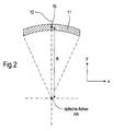
- this object is achieved by a microlithography projection objective for short wavelengths, preferably ⁇ 193 nm, an entrance pupil and an exit pupil for imaging a Object field in an image field, which represents the segment of a ring field, comprises, the segment having an axis of symmetry and an extent perpendicular to the axis of symmetry and the extent at least 20, preferably 25 mm and a first, a second, a third, a fourth, a fifth and a sixth mirror in center Arrangement includes an optical axis, each of these mirrors has a usable area in which the light rays that pass through the Projection lens are guided, impinge and the diameter of the Usable area of the first, second, third, fourth, fifth and sixth Mirror depending on the numerical aperture NA at the Exit pupil ⁇ 1200mm * NA, preferably ⁇ 300 mm, the numerical aperture NA at the exit pupil of the invention Objective is greater than 0.1, preferably greater than 0.2, particularly preferred greater than 0.23. Under numerical aperture at the exit pupil
- the imaging Beams of rays meet telecentrically on the image plane.
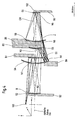
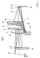
- the sixth mirror of the projection lens S6 has a concave shape.
- the fifth mirror S5 lies between the sixth mirror S6 and the Image plane.
- a shading-free Beam path in the lens realized in that with increasing numerical aperture at the exit pupil also the mean radius of the ring field to be imaged grows.
- a shading-free beam path is achieved in the above-mentioned areas on the fifth and sixth mirror in paraxial approximation if the mean ring field radius, depending on the numerical aperture NA at the exit pupil, the distances between the mirror apexes of the fifth and sixth mirrors (S5 S6), the distance of the fifth mirror and image plane (S5B), the radius of curvature r 5 , r 6 of the fifth and sixth mirror respectively is chosen. If the condition of an obscuration-free beam path is maintained, falling below the minimum radius leads to a sudden increase in the aspherical deviation from the spherical basic shape of the mirror, which is also referred to as the asphericity of the mirror. This applies in particular to the fifth mirror. This leaves the area for which the paraxial approximation and the aforementioned formula apply. However, mirrors with high asphericity can only be produced with great effort in terms of production technology.
- the first mirror is convex and all six mirrors are aspherical.
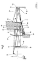
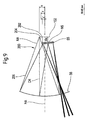
- two mirror segments are exemplary of the overall system 20, 22 of a projection lens according to the invention, the Mirror segments 20, 22 with the useful areas of the mirror correspond.
- the mirror segments are along an optical axis 24 arranged.
- everyone Usable area 20, 22 of a mirror of the projection lens a space 26, 28 assigned.
- Below the depth T of the installation space is in the present Registration of the expansion of the installation space from the center 30, 32 of the Usable area 20, 22 of each mirror parallel to the optical axis Roger that.
- As the center of the useful area in this Registration of the point of impact of the main beam CR of the central Field point of the object field on the useful area of the respective mirror Roger that.
- the mirrors in the Projection lens arranged such that the installation spaces 26, 28th not penetrate geometrically.
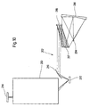
- the plane into which the object 100 through the inventive Projection lens is imaged the image plane 102 in which for example, a wafer can be arranged.
- the invention Projection objective comprises a first mirror S1, a second mirror S2, a third mirror S3, a fourth mirror S4, a fifth Mirror S5 and a sixth mirror S6.
- a first mirror S1 is a convex mirror.
- the installation space B1 to B4 and B6 of the mirrors S1 to S4 and S6 is at least 50 mm, the installation space B5 of the fifth mirror at least one Third of the diameter of the useful area of the fifth mirror, so that a free working distance between the next fifth mirror S5 and the image plane 102 of at least 12 mm is guaranteed.
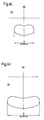
- FIGS. 6a to 6f The usable areas in the x-y plane of the respective mirror of the second
- the exemplary embodiment according to FIG. 5 is shown in FIGS. 6a to 6f.
- the x-y coordinate system is shown in all figures, such as defined by the object plane.
- the y direction denotes the Direction in the direction of the scan direction of a ring field scanner and the x direction the direction perpendicular to the scan direction.
- the useful area N3 is again kidney-shaped Diameter D is 102.367 mm according to FIG. 6c and for mirror S4 the useful area N4 according to FIG. 6d has a diameter of 222.497 mm on.
Landscapes
- Physics & Mathematics (AREA)
- General Physics & Mathematics (AREA)
- Optics & Photonics (AREA)
- Lenses (AREA)
Priority Applications (4)
| Application Number | Priority Date | Filing Date | Title |
|---|---|---|---|
| JP2001232558A JP2002107630A (ja) | 2000-08-01 | 2001-07-31 | 6枚の反射鏡を用いたマイクロリソグラフィ用の投影光学系 |
| KR1020010046237A KR100787525B1 (ko) | 2000-08-01 | 2001-07-31 | 6 거울-마이크로리소그래피 - 투사 대물렌즈 |
| TW090118732A TW538257B (en) | 2000-08-01 | 2001-08-01 | Microlithography projection objective |
| US09/920,285 US6867913B2 (en) | 2000-02-14 | 2001-08-01 | 6-mirror microlithography projection objective |
Applications Claiming Priority (2)
| Application Number | Priority Date | Filing Date | Title |
|---|---|---|---|
| DE10037870 | 2000-08-01 | ||
| DE10037870A DE10037870A1 (de) | 2000-08-01 | 2000-08-01 | 6-Spiegel-Mikrolithographie-Projektionsobjektiv |
Publications (3)
| Publication Number | Publication Date |
|---|---|
| EP1178356A2 true EP1178356A2 (fr) | 2002-02-06 |
| EP1178356A3 EP1178356A3 (fr) | 2003-05-28 |
| EP1178356B1 EP1178356B1 (fr) | 2004-09-22 |
Family
ID=7651213
Family Applications (1)
| Application Number | Title | Priority Date | Filing Date |
|---|---|---|---|
| EP01116916A Expired - Lifetime EP1178356B1 (fr) | 2000-02-14 | 2001-07-11 | Système de projection à six miroirs pour la microlithographie |
Country Status (2)
| Country | Link |
|---|---|
| EP (1) | EP1178356B1 (fr) |
| DE (2) | DE10037870A1 (fr) |
Cited By (10)
| Publication number | Priority date | Publication date | Assignee | Title |
|---|---|---|---|---|
| WO2002048796A3 (fr) * | 2000-12-12 | 2003-01-23 | Carl Zeiss Semiconductor Mfg | Systeme de projection pour lithographie euv |
| EP1418467A2 (fr) | 2002-11-08 | 2004-05-12 | Canon Kabushiki Kaisha | Système optique de projection, appareil d'exposition, et méthode de fabrication d'un dispositif |
| US6985210B2 (en) | 1999-02-15 | 2006-01-10 | Carl Zeiss Smt Ag | Projection system for EUV lithography |
| EP1642538A3 (fr) * | 2004-09-29 | 2006-05-17 | Karl Storz GmbH & Co. KG | Dispositif pour guider un outil de forage |
| WO2006117122A1 (fr) * | 2005-05-03 | 2006-11-09 | Carl Zeiss Smt Ag | Appareil d'exposition microlithographique utilisant une lumiere polarisee et systeme de projection microlithographique equipe de miroirs concaves primaire et secondaire |
| CN100399099C (zh) * | 2007-04-25 | 2008-07-02 | 北京航空航天大学 | 一种用于点光源汇聚成像的光学镜头 |
| USRE42118E1 (en) * | 1999-02-15 | 2011-02-08 | Carl-Zeiss-Smt Ag | Projection system for EUV lithography |
| US8072700B2 (en) | 2003-10-29 | 2011-12-06 | Carl Zeiss Smt Gmbh | Optical apparatus for use in photolithography |
| WO2017009096A1 (fr) | 2015-07-15 | 2017-01-19 | Carl Zeiss Smt Gmbh | Agencement de miroirs pour appareil d'exposition lithographique et système optique comprenant l'agencement de miroirs |
| US10754132B2 (en) | 2010-09-30 | 2020-08-25 | Carl Zeiss Smt Gmbh | Imaging optical system for microlithography |
Families Citing this family (4)
| Publication number | Priority date | Publication date | Assignee | Title |
|---|---|---|---|---|
| DE10240002A1 (de) | 2002-08-27 | 2004-03-11 | Carl Zeiss Semiconductor Manufacturing Technologies Ag | Optisches Teilsystem insbesondere für eine Projektionsbelichtungsanlage mit mindestens einem in mindestens zwei Stellungen verbringbaren optischen Element |
| KR101052386B1 (ko) * | 2003-09-27 | 2011-07-28 | 칼 짜이스 에스엠테 게엠베하 | 영점 교차 온도 근처에서 열팽창 계수의 온도에 따라, 상이한 기울기 부호를 갖는 재료로 구성된 미러들을 구비한 초단파 자외선 투영 광학계 |
| US7522260B1 (en) | 2004-09-29 | 2009-04-21 | Carl Zeiss Smt Ag | Method for correcting astigmatism in a microlithography projection exposure apparatus, a projection objective of such a projection exposure apparatus, and a fabrication method for micropatterned components |
| KR101370203B1 (ko) | 2005-11-10 | 2014-03-05 | 칼 짜이스 에스엠테 게엠베하 | 광원의 요동을 측정하기 위한 시스템을 구비한 euv 조명시스템 |
Family Cites Families (2)
| Publication number | Priority date | Publication date | Assignee | Title |
|---|---|---|---|---|
| JP2000100694A (ja) * | 1998-09-22 | 2000-04-07 | Nikon Corp | 反射縮小投影光学系、該光学系を備えた投影露光装置および該装置を用いた露光方法 |
| EP1772775B1 (fr) * | 1999-02-15 | 2008-11-05 | Carl Zeiss SMT AG | Dispositif à objectif de réduction pour la microlithographique ainsi qu'une installation d'éclairage à projection |
-
2000
- 2000-08-01 DE DE10037870A patent/DE10037870A1/de not_active Withdrawn
-
2001
- 2001-07-11 DE DE50103723T patent/DE50103723D1/de not_active Expired - Fee Related
- 2001-07-11 EP EP01116916A patent/EP1178356B1/fr not_active Expired - Lifetime
Cited By (17)
| Publication number | Priority date | Publication date | Assignee | Title |
|---|---|---|---|---|
| USRE42118E1 (en) * | 1999-02-15 | 2011-02-08 | Carl-Zeiss-Smt Ag | Projection system for EUV lithography |
| US6985210B2 (en) | 1999-02-15 | 2006-01-10 | Carl Zeiss Smt Ag | Projection system for EUV lithography |
| US7355678B2 (en) | 1999-02-15 | 2008-04-08 | Carl Zeiss Smt Ag | Projection system for EUV lithography |
| US7375798B2 (en) | 1999-02-15 | 2008-05-20 | Carl Zeiss Smt Ag | Projection system for EUV lithography |
| WO2002048796A3 (fr) * | 2000-12-12 | 2003-01-23 | Carl Zeiss Semiconductor Mfg | Systeme de projection pour lithographie euv |
| EP1418467A2 (fr) | 2002-11-08 | 2004-05-12 | Canon Kabushiki Kaisha | Système optique de projection, appareil d'exposition, et méthode de fabrication d'un dispositif |
| EP1418467A3 (fr) * | 2002-11-08 | 2005-11-23 | Canon Kabushiki Kaisha | Système optique de projection, appareil d'exposition, et méthode de fabrication d'un dispositif |
| US7119880B2 (en) | 2002-11-08 | 2006-10-10 | Canon Kabushiki Kaisha | Projection optical system, exposure apparatus, and device manufacturing method |
| US9933707B2 (en) | 2003-10-29 | 2018-04-03 | Carl Zeiss Smt Ag | Optical apparatus for use in photolithography |
| US8072700B2 (en) | 2003-10-29 | 2011-12-06 | Carl Zeiss Smt Gmbh | Optical apparatus for use in photolithography |
| EP1642538A3 (fr) * | 2004-09-29 | 2006-05-17 | Karl Storz GmbH & Co. KG | Dispositif pour guider un outil de forage |
| WO2006117122A1 (fr) * | 2005-05-03 | 2006-11-09 | Carl Zeiss Smt Ag | Appareil d'exposition microlithographique utilisant une lumiere polarisee et systeme de projection microlithographique equipe de miroirs concaves primaire et secondaire |
| CN100399099C (zh) * | 2007-04-25 | 2008-07-02 | 北京航空航天大学 | 一种用于点光源汇聚成像的光学镜头 |
| US10754132B2 (en) | 2010-09-30 | 2020-08-25 | Carl Zeiss Smt Gmbh | Imaging optical system for microlithography |
| WO2017009096A1 (fr) | 2015-07-15 | 2017-01-19 | Carl Zeiss Smt Gmbh | Agencement de miroirs pour appareil d'exposition lithographique et système optique comprenant l'agencement de miroirs |
| DE102015213275A1 (de) | 2015-07-15 | 2017-01-19 | Carl Zeiss Smt Gmbh | Spiegelanordnung für eine Lithographiebelichtungsanlage und Spiegelanordnung umfassendes optisches System |
| US10684466B2 (en) | 2015-07-15 | 2020-06-16 | Carl Zeiss Smt Gmbh | Mirror arrangement for lithography exposure apparatus and optical system comprising mirror arrangement |
Also Published As
| Publication number | Publication date |
|---|---|
| DE50103723D1 (de) | 2004-10-28 |
| DE10037870A1 (de) | 2002-02-14 |
| EP1178356A3 (fr) | 2003-05-28 |
| EP1178356B1 (fr) | 2004-09-22 |
Similar Documents
| Publication | Publication Date | Title |
|---|---|---|
| EP1772775B1 (fr) | Dispositif à objectif de réduction pour la microlithographique ainsi qu'une installation d'éclairage à projection | |
| EP1282011B1 (fr) | Lentille de projection réflective pour la photolithographie dans l'ultraviolet extrême | |
| DE69030231T2 (de) | Vorrichtung für Halbleiterlithographie | |
| DE69122018T2 (de) | Röntgenstrahllithographie mit ringförmigem Bildfeld | |
| EP1199590A1 (fr) | Lentille de projection microlithographique à 8 miroirs | |
| WO2002033467A1 (fr) | Objectif de projection par microlithographie a 8 miroirs | |
| EP1480082A1 (fr) | Système de quatre miroirs à champ annulaire pour lithographie EUV | |
| EP1845417B1 (fr) | Système d'éclairage doté d'un objectif à zoom | |
| DE102008042917A1 (de) | Abbildende Optik sowie Projektionsbelichtungsanlage für die Mikrolithographie mit einer derartigen abbildenden Optik | |
| EP1178356B1 (fr) | Système de projection à six miroirs pour la microlithographie | |
| DE10139177A1 (de) | Objektiv mit Pupillenobskuration | |
| EP1840622A2 (fr) | Objectif de projection et installation d'exposition de projection à distance focale négative de la pupille d'entrée | |
| DE102005042005A1 (de) | Hochaperturiges Objektiv mit obskurierter Pupille | |
| DE102014218474A1 (de) | Projektionsobjektiv, Projektionsbelichtungsanlage und Projektionsbelichtungsverfahren für die EUV-Mikrolithographie | |
| EP1102100A2 (fr) | Objectif catadioptrique avec diviseur de faisceau | |
| DE102018214437A1 (de) | Abbildende Optik zur Abbildung eines Objektfeldes in ein Bildfeld sowie Projektionsbelichtungsanlage mit einer derartigen abbildenden Optik | |
| DE69132160T2 (de) | Lithographie mit ringförmigen Bildfeld | |
| DE102009047179B4 (de) | Projektionsobjetiv | |
| DE102006043251A1 (de) | Mikrolithographie-Projektionsobjektiv, Projektionsbelichtungsanlage mit einem derartigen Objektiv, Herstellungsverfahren mikrostrukturierter Bauteile mit einer derartigen Projektionsbelichtungsanlage sowie mit diesem Verfahren hergestelltes Bauteil | |
| EP1037115B1 (fr) | Objectif de projection microlithographique et appareil d' exposition par projection | |
| DE102022210356A1 (de) | Optisches system, lithographieanlage mit einem optischen system und verfahren zum herstellen eines optischen systems | |
| DE102016205617A1 (de) | Projektionsbelichtungsverfahren und Projektionsbelichtungsanlage | |
| DE19948240A1 (de) | Mikrolithographie-Reduktionsobjektiveinrichtung sowie Projektionsbelichtungsanlage | |
| DE102016205618A1 (de) | Projektionsobjektiv mit Wellenfrontmanipulator, Projektionsbelichtungsverfahren und Projektionsbelichtungsanlage | |
| WO2003050587A2 (fr) | Objectif catadioptrique |
Legal Events
| Date | Code | Title | Description |
|---|---|---|---|
| PUAI | Public reference made under article 153(3) epc to a published international application that has entered the european phase |
Free format text: ORIGINAL CODE: 0009012 |
|
| AK | Designated contracting states |
Kind code of ref document: A2 Designated state(s): AT BE CH CY DE DK ES FI FR GB GR IE IT LI LU MC NL PT SE TR |
|
| AX | Request for extension of the european patent |
Free format text: AL;LT;LV;MK;RO;SI |
|
| PUAL | Search report despatched |
Free format text: ORIGINAL CODE: 0009013 |
|
| AK | Designated contracting states |
Designated state(s): AT BE CH CY DE DK ES FI FR GB GR IE IT LI LU MC NL PT SE TR |
|
| AX | Request for extension of the european patent |
Extension state: AL LT LV MK RO SI |
|
| 17P | Request for examination filed |
Effective date: 20031104 |
|
| AKX | Designation fees paid |
Designated state(s): DE FR GB IE NL |
|
| GRAP | Despatch of communication of intention to grant a patent |
Free format text: ORIGINAL CODE: EPIDOSNIGR1 |
|
| GRAS | Grant fee paid |
Free format text: ORIGINAL CODE: EPIDOSNIGR3 |
|
| RAP1 | Party data changed (applicant data changed or rights of an application transferred) |
Owner name: CARL ZEISS SMT AG |
|
| GRAA | (expected) grant |
Free format text: ORIGINAL CODE: 0009210 |
|
| AK | Designated contracting states |
Kind code of ref document: B1 Designated state(s): DE FR GB IE NL |
|
| PG25 | Lapsed in a contracting state [announced via postgrant information from national office to epo] |
Ref country code: FR Free format text: LAPSE BECAUSE OF FAILURE TO SUBMIT A TRANSLATION OF THE DESCRIPTION OR TO PAY THE FEE WITHIN THE PRESCRIBED TIME-LIMIT Effective date: 20040922 Ref country code: IE Free format text: LAPSE BECAUSE OF FAILURE TO SUBMIT A TRANSLATION OF THE DESCRIPTION OR TO PAY THE FEE WITHIN THE PRESCRIBED TIME-LIMIT Effective date: 20040922 Ref country code: GB Free format text: LAPSE BECAUSE OF FAILURE TO SUBMIT A TRANSLATION OF THE DESCRIPTION OR TO PAY THE FEE WITHIN THE PRESCRIBED TIME-LIMIT Effective date: 20040922 |
|
| REG | Reference to a national code |
Ref country code: GB Ref legal event code: FG4D Free format text: NOT ENGLISH |
|
| REG | Reference to a national code |
Ref country code: IE Ref legal event code: FG4D Free format text: GERMAN |
|
| REF | Corresponds to: |
Ref document number: 50103723 Country of ref document: DE Date of ref document: 20041028 Kind code of ref document: P |
|
| GBV | Gb: ep patent (uk) treated as always having been void in accordance with gb section 77(7)/1977 [no translation filed] |
Effective date: 20040922 |
|
| REG | Reference to a national code |
Ref country code: IE Ref legal event code: FD4D |
|
| PLBE | No opposition filed within time limit |
Free format text: ORIGINAL CODE: 0009261 |
|
| STAA | Information on the status of an ep patent application or granted ep patent |
Free format text: STATUS: NO OPPOSITION FILED WITHIN TIME LIMIT |
|
| 26N | No opposition filed |
Effective date: 20050623 |
|
| EN | Fr: translation not filed | ||
| PGFP | Annual fee paid to national office [announced via postgrant information from national office to epo] |
Ref country code: DE Payment date: 20080722 Year of fee payment: 8 |
|
| PG25 | Lapsed in a contracting state [announced via postgrant information from national office to epo] |
Ref country code: DE Free format text: LAPSE BECAUSE OF NON-PAYMENT OF DUE FEES Effective date: 20100202 |
|
| PGFP | Annual fee paid to national office [announced via postgrant information from national office to epo] |
Ref country code: NL Payment date: 20150721 Year of fee payment: 15 |
|
| REG | Reference to a national code |
Ref country code: NL Ref legal event code: MM Effective date: 20160801 |
|
| PG25 | Lapsed in a contracting state [announced via postgrant information from national office to epo] |
Ref country code: NL Free format text: LAPSE BECAUSE OF NON-PAYMENT OF DUE FEES Effective date: 20160801 |