EP1178527A2 - Procédé d'enlèvement de carbure de silicium de substrats semiconducteurs par oxydation - Google Patents
Procédé d'enlèvement de carbure de silicium de substrats semiconducteurs par oxydation Download PDFInfo
- Publication number
- EP1178527A2 EP1178527A2 EP01118611A EP01118611A EP1178527A2 EP 1178527 A2 EP1178527 A2 EP 1178527A2 EP 01118611 A EP01118611 A EP 01118611A EP 01118611 A EP01118611 A EP 01118611A EP 1178527 A2 EP1178527 A2 EP 1178527A2
- Authority
- EP
- European Patent Office
- Prior art keywords
- substrate
- silicon carbide
- silicon oxide
- oxygen
- etch
- Prior art date
- Legal status (The legal status is an assumption and is not a legal conclusion. Google has not performed a legal analysis and makes no representation as to the accuracy of the status listed.)
- Withdrawn
Links
Images


Classifications
-
- H—ELECTRICITY
- H10—SEMICONDUCTOR DEVICES; ELECTRIC SOLID-STATE DEVICES NOT OTHERWISE PROVIDED FOR
- H10P—GENERIC PROCESSES OR APPARATUS FOR THE MANUFACTURE OR TREATMENT OF DEVICES COVERED BY CLASS H10
- H10P95/00—Generic processes or apparatus for manufacture or treatments not covered by the other groups of this subclass
-
- H—ELECTRICITY
- H10—SEMICONDUCTOR DEVICES; ELECTRIC SOLID-STATE DEVICES NOT OTHERWISE PROVIDED FOR
- H10P—GENERIC PROCESSES OR APPARATUS FOR THE MANUFACTURE OR TREATMENT OF DEVICES COVERED BY CLASS H10
- H10P50/00—Etching of wafers, substrates or parts of devices
- H10P50/20—Dry etching; Plasma etching; Reactive-ion etching
- H10P50/28—Dry etching; Plasma etching; Reactive-ion etching of insulating materials
- H10P50/282—Dry etching; Plasma etching; Reactive-ion etching of insulating materials of inorganic materials
- H10P50/283—Dry etching; Plasma etching; Reactive-ion etching of insulating materials of inorganic materials by chemical means
-
- H—ELECTRICITY
- H10—SEMICONDUCTOR DEVICES; ELECTRIC SOLID-STATE DEVICES NOT OTHERWISE PROVIDED FOR
- H10D—INORGANIC ELECTRIC SEMICONDUCTOR DEVICES
- H10D62/00—Semiconductor bodies, or regions thereof, of devices having potential barriers
- H10D62/80—Semiconductor bodies, or regions thereof, of devices having potential barriers characterised by the materials
- H10D62/83—Semiconductor bodies, or regions thereof, of devices having potential barriers characterised by the materials being Group IV materials, e.g. B-doped Si or undoped Ge
- H10D62/832—Semiconductor bodies, or regions thereof, of devices having potential barriers characterised by the materials being Group IV materials, e.g. B-doped Si or undoped Ge being Group IV materials comprising two or more elements, e.g. SiGe
- H10D62/8325—Silicon carbide
-
- H—ELECTRICITY
- H10—SEMICONDUCTOR DEVICES; ELECTRIC SOLID-STATE DEVICES NOT OTHERWISE PROVIDED FOR
- H10P—GENERIC PROCESSES OR APPARATUS FOR THE MANUFACTURE OR TREATMENT OF DEVICES COVERED BY CLASS H10
- H10P14/00—Formation of materials, e.g. in the shape of layers or pillars
- H10P14/60—Formation of materials, e.g. in the shape of layers or pillars of insulating materials
- H10P14/63—Formation of materials, e.g. in the shape of layers or pillars of insulating materials characterised by the formation processes
- H10P14/6302—Non-deposition formation processes
- H10P14/6304—Formation by oxidation, e.g. oxidation of the substrate
-
- H—ELECTRICITY
- H10—SEMICONDUCTOR DEVICES; ELECTRIC SOLID-STATE DEVICES NOT OTHERWISE PROVIDED FOR
- H10P—GENERIC PROCESSES OR APPARATUS FOR THE MANUFACTURE OR TREATMENT OF DEVICES COVERED BY CLASS H10
- H10P14/00—Formation of materials, e.g. in the shape of layers or pillars
- H10P14/60—Formation of materials, e.g. in the shape of layers or pillars of insulating materials
- H10P14/63—Formation of materials, e.g. in the shape of layers or pillars of insulating materials characterised by the formation processes
- H10P14/6302—Non-deposition formation processes
- H10P14/6304—Formation by oxidation, e.g. oxidation of the substrate
- H10P14/6306—Formation by oxidation, e.g. oxidation of the substrate of the semiconductor materials
- H10P14/6308—Formation by oxidation, e.g. oxidation of the substrate of the semiconductor materials of Group IV semiconductors
Definitions
- the invention generally relates to semiconductor wafer processing equipment and, more particularly, to a method and apparatus for removing silicon carbide from semiconductor substrates.
- silicon carbide is difficult and expensive to remove.
- Traditional methods of removing material from substrates, such as etching with hydrofluoric acid, are time consuming and costly when used to remove silicon carbide.
- using hydrofluoric acid to etch silicon carbide causes organic polymer formation on the substrates. Such polymer formation changes the surface composition of the substrates and renders the substrates unusable for further test processing. Removing silicon carbide while preserving uniformity of substrate thickness and surface composition is a problem frequently encountered in the microelectronic device fabrication industry.
- the present invention provides a method and apparatus for removing silicon carbide from substrates.
- the invention provides a method in which silicon carbide on a substrate is oxidized to form a silicon oxide, and then the silicon oxide is removed.
- the present invention generally provides a method and apparatus for removing silicon carbide from substrates.
- silicon carbide on a substrate is oxidized to form a silicon oxide and then the silicon oxide is removed from the substrate.
- the silicon oxide can be much more readily removed than the silicon carbide using conventional cleaning techniques such as etching using a hydrofluoric acid solution.
- the substrate is left with a thickness and surface composition substantially similar to that of the substrate prior to the processing leading to the silicon carbide being deposited. Assuming the substrate is being used for test processing purposes, the substrate is, at this point, ready to be reused for additional test processing.
- Silicon carbide may be removed from a test substrate many times in this manner, while preserving the necessary consistency with regard to substrate thickness and surface composition required for test processing purposes.
- the average thickness of the substrate after silicon carbide removal is within 2% of the average thickness of the substrate prior to deposition of the silicon carbide.
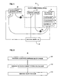
- FIG. 1 depicts a block diagram of a system 20 for removing silicon carbide from substrates, where the silicon carbide has been deposited by chamber 42.
- the silicon carbide removal system 20 comprises an oxidation chamber 30 and a silicon oxide etch system 32.
- the silicon oxide etch system 32 may comprise an etch station 34, a clean station 36, and a centrifuge 38.
- the substrate 22 2 (comprising silicon carbide) is transferred to the oxidation chamber 30, where the silicon carbide is oxidized to form a silicon oxide.
- the substrate 22 3 (comprising silicon oxide) is transferred to the etch station 34. After etching of the silicon oxide in the etch station 34, the substrate is transferred to the clean station 36, where the substrate is cleaned and the etch process is stopped. Finally, the substrate is spin dried in the centrifuge 38. At this point, if the substrate is a test substrate to be reused for additional test processing, the clean substrate 22 1 may be transferred back to the silicon carbide deposition chamber 42.
- the process for removing silicon carbide from substrates is preferably controlled by a process controller 40, such as a programmable computer having one or more central processing units (CPUs) and support circuitry containing memory (a computer readable medium) for storing associated control software.
- a process controller 40 such as a programmable computer having one or more central processing units (CPUs) and support circuitry containing memory (a computer readable medium) for storing associated control software.
- CPUs central processing units
- a single process controller 40 may be used to control deposition, oxidation, and etching, or multiple process controllers may be used.
- FIG. 2 shows a general process flow diagram for a method 50 of removing silicon carbide from substrates.
- a substrate comprising silicon carbide is provided.
- the silicon carbide is generally in the form of a layer.
- the silicon carbide could be a feature on the substrate, such as a line, via, plug, pad, or the like.
- the silicon carbide is oxidized to form a silicon oxide.
- Step 102 can be performed by various processing techniques as discussed below with reference to FIGS. 3 and 4.
- the silicon oxide is removed. Step 104 may be accomplished by processing techniques as discussed below with reference to FIG. 3.
- FIG. 3 shows a process flow diagram for a first embodiment 150 of the method of FIG. 2.
- a substrate comprising silicon carbide is provided.
- the substrate is transferred to a substrate heating system, such as a furnace.
- the substrate may be transferred by an automated transfer robot, as is commonly known in the art.
- the substrate heating system heats the substrate in an oxygen atmosphere to oxidize the silicon carbide to form a silicon oxide.
- the silicon carbide comprises a layer having a thickness of up to about 5k ⁇ and the silicon oxide comprises a layer having a thickness of up to about 4k ⁇ .
- the substrate is transferred to a solvent etch system.
- the solvent etch system performs solvent etch processing of the substrate to remove the silicon oxide by immersion of the substrate in a solvent Conventional solvents such as a buffered hydrofluoric acid solution or other fluorine-based solvents may be used. Finally, in step 208, the substrate is removed from the solvent etch system.
- Step 202 may be implemented using a furnace, such as a vacuum furnace, as a heating system.
- a furnace such as a vacuum furnace
- the temperature of the interior of the furnace is raised to about 650°C, and the pressure kept at atmospheric pressure.
- nitrogen (N 2 ) gas is introduced into the furnace at a flow rate of about 7 standard liters per minute (slpm) while the temperature of the interior of the furnace is increased from about 650°C to about 1000°C at the rate of about 10°C to 20°C per minute.
- oxygen gas O 2
- a hydrogen and oxygen gas mixture is introduced into the furnace by introducing oxygen gas at a flow rate of about 3.5 slpm and hydrogen gas at a flow rate of about 2 slpm.
- the substrate While flowing the hydrogen and oxygen into the furnace, the substrate is allowed to remain in the 1000°C furnace for from about 20 minutes to about 120 minutes depending on the quantity of silicon carbide to be removed, while the silicon carbide is oxidized to form a silicon oxide.
- the substrate is heated for about 30 minutes.
- the substrate is heated for about 45 minutes.
- the substrate is heated for about 90 minutes. During this process, carbon dioxide and water are formed and exhausted from the furnace.
- the hydrogen gas flow into the chamber is stopped, and oxygen is introduced into the chamber at a flow rate of about 2 slpm for about one minute.
- the oxygen flow is stopped and nitrogen gas is introduced into the chamber at a flow rate of about 7 slpm while the temperature is decreased from about 1000°C to about 650°C at the rate of about 10°C to 20°C per minute.
- the substrate is removed from the furnace.
- the quantities in the above example are variable within certain ranges and depending upon certain factors.
- the oxidation temperature which is 1000°C in the above example, may range from about 650°C to about 1050°C.
- the ratio of introduced hydrogen gas to introduced oxygen gas may vary.
- a liters-of-hydrogen to liters-of-oxygen ratio of between about 2-to-1 and about 1.75-to-1 is preferred. More particularly, if the oxidation process takes place in a vacuum furnace, a liters-of-hydrogen to liters-of-oxygen ratio of about 2-to-1 is preferred.
- the following process may be used to implement step 206, wherein a solvent etch system performs solvent etch processing on the substrate to remove silicon oxide.
- the solvent etch system may comprise a hydrofluoric acid bath, a deionized water bath, and a centrifuge.
- the hydrofluoric acid bath contains a buffered 49% solution of hydrofluoric acid.
- the substrate is first placed in the hydrofluoric acid bath and allowed to soak in the hydrofluoric acid bath for about 20 minutes to etch any silicon oxide from the substrate.
- the substrate is immersed in a deionized water bath for about 5 minutes to stop the etch process and clean the substrate. After this, the substrate is spin dried for about 5 minutes in the centrifuge.
- the substrate is removed from the solvent etch system (step 208).
- Fig. 4 shows a process flow diagram for a second embodiment 250 of the method of FIG. 2.
- oxidation of the silicon carbide is achieved through plasma oxidation processing in a plasma oxidation processing system comprising a plasma oxidation processing chamber.
- a substrate comprising silicon carbide is provided.
- the substrate is transferred to a plasma oxidation processing system.
- the substrate may be transferred by an automated transfer robot, as is commonly known in the art.
- plasma oxidation processing is performed on the substrate in the plasma oxidation processing chamber of the plasma oxidation processing system to oxidize the silicon carbide to form a silicon oxide.
- the plasma oxidation processing may utilize a high power RF source (i.e., 500W or greater) to generate a high temperature (i.e., greater than 300°C) plasma from a gas that may comprise fluorine and oxygen.
- Solvent etching of the silicon oxide is performed in the same manner as discussed with regard to FIG. 2. Specifically, at step 204, the substrate is transferred to a solvent etch system. At step 206, solvent etching is performed on the substrate to remove the silicon oxide. Finally, in step 208, the substrate is removed from the solvent etch system.
Landscapes
- Drying Of Semiconductors (AREA)
- Formation Of Insulating Films (AREA)
- Cleaning Or Drying Semiconductors (AREA)
Applications Claiming Priority (2)
| Application Number | Priority Date | Filing Date | Title |
|---|---|---|---|
| US63307800A | 2000-08-04 | 2000-08-04 | |
| US633078 | 2000-08-04 |
Publications (2)
| Publication Number | Publication Date |
|---|---|
| EP1178527A2 true EP1178527A2 (fr) | 2002-02-06 |
| EP1178527A3 EP1178527A3 (fr) | 2006-09-27 |
Family
ID=24538193
Family Applications (1)
| Application Number | Title | Priority Date | Filing Date |
|---|---|---|---|
| EP01118611A Withdrawn EP1178527A3 (fr) | 2000-08-04 | 2001-08-02 | Procédé d'enlèvement de carbure de silicium de substrats semiconducteurs par oxydation |
Country Status (3)
| Country | Link |
|---|---|
| EP (1) | EP1178527A3 (fr) |
| JP (1) | JP2002151505A (fr) |
| KR (1) | KR20020017959A (fr) |
Cited By (1)
| Publication number | Priority date | Publication date | Assignee | Title |
|---|---|---|---|---|
| US20110309376A1 (en) * | 2010-06-16 | 2011-12-22 | Sumitomo Electric Industries, Ltd. | Method of cleaning silicon carbide semiconductor, silicon carbide semiconductor, and silicon carbide semiconductor device |
Families Citing this family (1)
| Publication number | Priority date | Publication date | Assignee | Title |
|---|---|---|---|---|
| CN110858540A (zh) * | 2018-08-22 | 2020-03-03 | 株洲中车时代电气股份有限公司 | 一种碳化硅u型槽的制备方法 |
Family Cites Families (8)
| Publication number | Priority date | Publication date | Assignee | Title |
|---|---|---|---|---|
| JP2523558B2 (ja) * | 1986-12-26 | 1996-08-14 | 株式会社日立製作所 | 処理方法 |
| US5305221A (en) * | 1990-05-04 | 1994-04-19 | Atherton Robert W | Real world modeling and control process for integrated manufacturing equipment |
| JPH0529296A (ja) * | 1991-07-24 | 1993-02-05 | Nec Corp | ウエツト処理装置 |
| US5723376A (en) * | 1994-06-23 | 1998-03-03 | Nippondenso Co., Ltd. | Method of manufacturing SiC semiconductor device having double oxide film formation to reduce film defects |
| JPH08162408A (ja) * | 1994-12-08 | 1996-06-21 | Nec Corp | 半導体装置の製造方法 |
| JPH10199848A (ja) * | 1997-01-09 | 1998-07-31 | Mitsui Eng & Shipbuild Co Ltd | 炭化ケイ素ウエハの表面汚染除去方法および炭化ケイ素ウエハ |
| DE19829309B4 (de) * | 1997-07-04 | 2008-02-07 | Fuji Electric Co., Ltd., Kawasaki | Verfahren zur Herstellung eines thermischen Oxidfilms auf Siliciumcarbid |
| KR20020028047A (ko) * | 1999-05-03 | 2002-04-15 | 맥켈러 로버트 루이스 | 실리콘 카바이드 제거 방법 |
-
2001
- 2001-08-02 EP EP01118611A patent/EP1178527A3/fr not_active Withdrawn
- 2001-08-03 KR KR1020010046996A patent/KR20020017959A/ko not_active Withdrawn
- 2001-08-06 JP JP2001237979A patent/JP2002151505A/ja not_active Withdrawn
Cited By (1)
| Publication number | Priority date | Publication date | Assignee | Title |
|---|---|---|---|---|
| US20110309376A1 (en) * | 2010-06-16 | 2011-12-22 | Sumitomo Electric Industries, Ltd. | Method of cleaning silicon carbide semiconductor, silicon carbide semiconductor, and silicon carbide semiconductor device |
Also Published As
| Publication number | Publication date |
|---|---|
| JP2002151505A (ja) | 2002-05-24 |
| KR20020017959A (ko) | 2002-03-07 |
| EP1178527A3 (fr) | 2006-09-27 |
Similar Documents
| Publication | Publication Date | Title |
|---|---|---|
| US20060102208A1 (en) | System for removing a residue from a substrate using supercritical carbon dioxide processing | |
| JP6242933B2 (ja) | 基板処理装置、半導体装置の製造方法およびプログラム | |
| US20060102204A1 (en) | Method for removing a residue from a substrate using supercritical carbon dioxide processing | |
| KR102118784B1 (ko) | 산화막 제거 방법 및 제거 장치, 그리고 컨택트 형성 방법 및 컨택트 형성 시스템 | |
| US9177781B2 (en) | Plasma processing method and manufacturing method of semiconductor device | |
| JP2001176855A (ja) | 基板処理方法および基板処理装置 | |
| US20100024840A1 (en) | Chamber plasma-cleaning process scheme | |
| JP4789821B2 (ja) | 基板処理装置の検査方法 | |
| EP0946978A1 (fr) | Traitement halogene/uv pour gravure par un oxyde anhydre | |
| JP3526284B2 (ja) | 基板表面の処理方法 | |
| EP1178527A2 (fr) | Procédé d'enlèvement de carbure de silicium de substrats semiconducteurs par oxydation | |
| US20040222191A1 (en) | Method and apparatus for wet etching using hot etchant | |
| JPH11330064A (ja) | 半導体装置の製造工程における薄膜形成方法 | |
| JP3058909B2 (ja) | クリーニング方法 | |
| US7659206B2 (en) | Removal of silicon oxycarbide from substrates | |
| JPH05326477A (ja) | 半導体基板表面のハロゲン除去方法 | |
| JPH06236864A (ja) | エッチング処理方法及びエッチングの後処理方法並びにエッチング設備 | |
| US20050284572A1 (en) | Heating system for load-lock chamber | |
| JPH08195382A (ja) | 半導体製造装置 | |
| US20020023663A1 (en) | Apparatus and method for preventing the re-adherence of particles in wafer-cleaning process | |
| JP4312198B2 (ja) | 薄膜形成装置の洗浄方法、薄膜形成装置及びプログラム | |
| JP2002025924A (ja) | 熱処理炉の空焼き方法 | |
| JPS6399533A (ja) | シリコン窒化膜のドライエツチング方法及びドライエツチング装置 | |
| JP2006165372A (ja) | 枚葉式洗浄装置および洗浄方法 | |
| JPH0917766A (ja) | 基板の洗浄方法 |
Legal Events
| Date | Code | Title | Description |
|---|---|---|---|
| PUAI | Public reference made under article 153(3) epc to a published international application that has entered the european phase |
Free format text: ORIGINAL CODE: 0009012 |
|
| AK | Designated contracting states |
Kind code of ref document: A2 Designated state(s): AT BE CH CY DE DK ES FI FR GB GR IE IT LI LU MC NL PT SE TR |
|
| AX | Request for extension of the european patent |
Free format text: AL;LT;LV;MK;RO;SI |
|
| PUAL | Search report despatched |
Free format text: ORIGINAL CODE: 0009013 |
|
| AK | Designated contracting states |
Kind code of ref document: A3 Designated state(s): AT BE CH CY DE DK ES FI FR GB GR IE IT LI LU MC NL PT SE TR |
|
| AX | Request for extension of the european patent |
Extension state: AL LT LV MK RO SI |
|
| AKX | Designation fees paid | ||
| STAA | Information on the status of an ep patent application or granted ep patent |
Free format text: STATUS: THE APPLICATION IS DEEMED TO BE WITHDRAWN |
|
| 18D | Application deemed to be withdrawn |
Effective date: 20070328 |
|
| REG | Reference to a national code |
Ref country code: DE Ref legal event code: 8566 |