EP1178537A2 - Bipolartransistor und Halbleiterbauelement - Google Patents
Bipolartransistor und Halbleiterbauelement Download PDFInfo
- Publication number
- EP1178537A2 EP1178537A2 EP01123874A EP01123874A EP1178537A2 EP 1178537 A2 EP1178537 A2 EP 1178537A2 EP 01123874 A EP01123874 A EP 01123874A EP 01123874 A EP01123874 A EP 01123874A EP 1178537 A2 EP1178537 A2 EP 1178537A2
- Authority
- EP
- European Patent Office
- Prior art keywords
- layer
- base
- emitter
- bipolar transistor
- collector
- Prior art date
- Legal status (The legal status is an assumption and is not a legal conclusion. Google has not performed a legal analysis and makes no representation as to the accuracy of the status listed.)
- Withdrawn
Links
Images






Classifications
-
- H—ELECTRICITY
- H10—SEMICONDUCTOR DEVICES; ELECTRIC SOLID-STATE DEVICES NOT OTHERWISE PROVIDED FOR
- H10D—INORGANIC ELECTRIC SEMICONDUCTOR DEVICES
- H10D10/00—Bipolar junction transistors [BJT]
- H10D10/80—Heterojunction BJTs
- H10D10/821—Vertical heterojunction BJTs
- H10D10/881—Resonant tunnelling transistors
Definitions
- the present invention relates to a semiconductor device having a heterojunction portion such as a bipolar transistor, a diode, or an I 2 L.
- a bipolar transistor Because of its excellent RF characteristics, a bipolar transistor has conventionally been used as an active device operable in the microwave/milliwave bands. In particular, most vigorous research and development has been directed to a heterojunction bipolar transistor (HBT) using a III-V compound semiconductor such as GaAs. In recent years, attention has been focused on a HBT using a SiGe material, which is a IV-IV compound material that can be fabricated on a low-cost silicon substrate.
- HBT heterojunction bipolar transistor
- One of the two types is a HBT reported in Document 1 (L. Harame et al., "Optimization of SiGe HBT Technology for High Speed Analog and Mixed-Signal Applications," IEDM Tech. Dig. 1993, p.71), which comprises a Si collector layer, a SiGe base layer, and a Si emitter layer.
- a Ge composition ratio is increased gradually from a region in contact with the Si emitter layer toward a region in contact with the Si collector layer to provide a graded composition base layer.
- the other of the two types is a HBT reported in Document 2 (A.
- Figure 18 is a band diagram of the former heterojunction bipolar transistor having the graded composition base layer.
- an electric field induced by the graded composition causes carriers injected into the SiGe base layer to drift in the SiGe base layer toward the collector layer. Since the traveling of the carriers caused by the drift electric field is at a higher speed than the traveling thereof caused by diffusion, a base transit time is reduced and excellent RF characteristics are obtained.
- Figure 19 is a band diagram of the latter heterojunction bipolar transistor having the uniform composition base structure.
- the base layer is extremely thinned to reduce the base transit time and provide excellent RF characteristics.
- the thinning of the base layer incurs the risk of increasing the base resistance, so that the base layer is doped with a high-concentration impurity to lower the base resistance.
- SiGe having a high Ge composition ratio is used in the base layer to prevent reverse injection of carriers from the base layer doped with the high-concentration impurity into the emitter, so that a heterojunction barrier formed between the SiGe base layer and the Si emitter layer is increased.
- excellent RF characteristics are obtained.
- the doping concentration in the base layer is increased to reduce the base resistance and thereby increase a maximum oscillation frequency.
- a conventional Si LSI using a bipolar transistor it has frequently been performed to compose a diode by using a PN junction portion between the base and collector of the NPN bipolar transistor and use the diode as an element of a logic circuit.
- the NPN bipolar transistor has a structure suitable for the formation of a large number of built-in diodes since the PN junction portion between the base and collector has a high breakdown voltage (with respect to a reverse bias) and the N-type collector layer is used as a common region in the substrate.
- a PN junction diode has the drawback that it is unsuitable for use in a device operating at a high speed due to minority carriers accumulated in each of the P-type and N-type regions thereof. Specifically, electrons as minority carriers are accumulated in the P-type base layer of the NPN bipolar transistor layer, while holes as minority carriers are accumulated in the N-type collector layer thereof.
- the P-type base layer is formed extremely thin to reduce the base transit time so that the accumulation of the electrons in the P-type base layer presents substantially no problem even in the PN junction diode composed by using a part of the bipolar transistor.
- the N-type collector layer is formed to have a sufficient thickness in the range of 0.5 to 1 ⁇ m in order to retain a high breakdown voltage, so that numerous holes are accumulated therein, which eventually limits the speed of the PN junction diode.
- the conventional HBT using the graded composition base shown in Figure 18 it is required to greatly vary the Ge composition ratio in order to increase the intensity of the drift electric field induced by the graded composition.
- the region of the base layer in contact with the emitter layer normally has a pure Si composition without containing Ge, so that the base/emitter PN junction forms a silicon/silicon homojunction.
- the quantity of carriers reversely injected into the emitter is increased because the base layer has no heterojunction barrier at all or, if any, an extremely low heterojunction barrier, so that the current amplification factor ⁇ is not increased.
- f max f T 8 ⁇ R B ⁇ C BC
- the fact that the current amplification factor ⁇ is not increased can also be derived from the relationship represented by the following equation (2), which is established among the current amplification factor ⁇ , the band discontinuity value ⁇ Ev of a valence band at the emitter/base junction portion, and a carrier concentration N B in the base layer.
- the conventional structure using the uniform composition base shown in Figure 19 can suppress reverse injection of carriers from the base layer because a high heterojunction barrier is formed between the SiGe base layer having a high Ge composition ratio and a Si emitter layer. If the concentration of carriers in the SiGe base layer (base doping concentration) is to be further increased in order to increase the maximum oscillation frequency fmax, as described above, the quantity of carriers reversely injected is increased. To prevent this, it is required to further enhance the height of the heterojunction barrier by further increasing the Ge composition ratio in the SiGe base layer, which increases the difference in lattice constant between the emitter layer and the base layer. As a result, a critical film thickness at which a dislocation occurs in the base layer presents a problem.
- the film thickness at which a dislocation occurs is generally termed the critical film thickness.
- the critical film thickness is smaller as the Ge composition ratio in the SiGe layer is higher.
- the critical film thickness is on the order of 50 nm when the Ge composition ratio is 30%, which corresponds to the film thickness of the base layer.
- the SiGe layer is not in a completely stable state but in a quasi-stable state if the Ge composition ratio is high. If a high-temperature process is performed in a subsequent step, such a defect as dislocation is easily caused. Hence, it is inappropriate in terms of device reliability and a thermal budget during a device fabrication process to use a SiGe layer having a high Ge composition ratio.
- the thickness of the base layer is preferably reduced to a value equal to or smaller than the critical film thickness and device reliability and the thermal budget during the device fabrication process should be ensured, as described above, a Ge composition ratio in the SiGe layer which is 25% or higher is excessively high in terms of reliability and manufacturability.
- a first object of the present invention is to provide a bipolar transistor wherein a current amplification factor is increased with the provision of a region having the function of suppressing reverse injection of carriers from the base layer into the emitter layer irrespective of a barrier formed at the emitter/base junction.
- the current amplification factor can be improved even when a base doping concentration is increased to increase the maximum oscillation frequency fmax by relaxing restrictions on the increase of the current amplification factor.
- a second object of the present invention is to provide an element functioning as a bipolar transistor, a diode, an I 2 L element, or the like which operates at a high speed by suppressing the injection of minority carriers from the base layer into the collector layer and thereby reducing the quantity of minority carriers accumulated in the collector layer.
- This can be achieved by providing means for effectively increasing a heterojunction barrier formed at the base/collector junction without increasing the Ge composition ratio in the SiGe base layer to such a value as to excessively reduce the critical film thickness, i.e., by implementing a structure which ensures sufficiently high reliability.
- a first bipolar transistor according to the present invention has a multi-quantum barrier (MQB) composed of a superlattice structure consisting of two types of extremely thin films having different compositions and alternately stacked, which is provided in a region of the emitter adjacent the emitter/base junction.
- the MQB reflects a wave of carriers reversely injected from the base, which fact is used to effectively increase the height of a hetero-junction barrier (barrier height) and thereby suppress the reverse injection of the carriers from the base layer.
- the first bipolar transistor has the following structure.
- the first bipolar transistor according to the present invention comprises an emitter layer, a base layer, and a collector layer, the bipolar transistor having a multi-quantum barrier portion being provided in the emitter layer and composed of a plurality of barrier layers and well layers alternately stacked to perform the function of reflecting an incident wave of minority carriers in the emitter layer injected from the base layer and provide such a phase that the incident wave of carriers and a reflected wave of carriers intensify each other.
- the traveling speed of carriers in the base layer is determined by a drift velocity, not by a diffusion speed, so that the base transit time is reduced and a current gain cut-off frequency fT is increased.
- the multi-quantum barrier portion suppresses reverse junction of carriers from the base layer into the emitter layer irrespective of the band discontinuity value reduced by the provision of the graded composition base.
- the critical film thickness of the Si 1-x-y Ge x C y layer at the multi-quantum barrier portion is particularly increased, so that it becomes possible to further increase the effective barrier height of the multi-quantum barrier portion without incurring a dislocation.
- the multi-quantum barrier portion being disposed in a region of the emitter layer exterior to a depletion region formed between the emitter layer and the base layer at a working voltage when the transistor is operating, the function of suppressing reverse injection of carriers from the base into the emitter can maximally be performed in any operating condition.
- the barrier layer at the end of the multi-quantum barrier portion closer to the base layer in such a position as to prevent the tunneling of the carriers from the depletion region formed between the emitter layer and the base layer to the well layer adjacent to the barrier layer at the end of the multi-quantum barrier portion closer to the base layer, such improved RF characteristics as described above can be expected without degrading the function of suppressing reverse injection of carriers performed by the multi-quantum barrier portion.
- a second bipolar according to the present invention has a high-concentration doped layer for effectively enhancing the function of suppressing reverse injection of carriers from the base layer into the emitter layer, which is provided in the emitter layer of the bipolar transistor.
- the second bipolar has the following structure.
- the second bipolar transistor according to the present invention comprises an emitter layer containing an impurity of a first conductivity type, a base layer containing an impurity of a second conductivity type, and a collector layer containing the impurity of the first conductivity type, the bipolar transistor having a high-concentration doped layer being provided in the emitter layer and doped with the impurity of the first conductivity type at a higher concentration than in the emitter layer.
- the high-concentration doped layer is a ⁇ - doped layer having a thickness of 10 nm or less.
- the concentration of carriers of the first conductivity type in the high-concentration doped layer is 1 x 10 19 cm -3 or more.
- the concentration of carriers of the first conductivity type in the high-concentration doped layer is more than ten times higher than the concentration of the carriers of the first conductivity type in the emitter layer.
- the high-concentration doped layer being adjacent to a depletion region formed at an emitter/base junction portion, there can maximally be performed the function of suppressing reverse injection of carriers from the base to the emitter.
- the concentration of carriers of the second conductivity type in the base layer is higher than the concentration of carriers of the first conductivity type in the emitter layer.
- the function of suppressing reverse injection of carriers from the base layer is further enhanced by using a high barrier at the heterojunction portion.
- the strained base layer achieves a particularly high effect when the difference in lattice constant between the emitter layer and the base layer is large.
- a semiconductor device has a multi-quantum barrier (MQB) having a superlattice structure consisting of two types of extremely thin films having different compositions and alternately stacked, which is provided in a region of the collector layer in contact with the collector/base junction.
- MQB multi-quantum barrier
- the height of the heterojunction barrier (barrier height) has been effectively increased by using the effect of reflecting a wave of carriers injected from the base (minority carriers in the collector layer).
- the semiconductor device has the following structure.
- the semiconductor device comprises a bipolar transistor comprises an emitter layer, a base layer, and a collector layer, the bipolar transistor having a multi-quantum barrier portion being provided in the collector layer and composed of a plurality of barrier layers and well layers alternately stacked to perform the function of reflecting an incident wave of minority carriers in the collector layer injected from the base layer (minority carriers in the collector layer) and provide such a phase that the incident wave and a reflected wave intensify each other.
- the carriers in the base layer are prevented from being injected into the collector layer not only by a barrier induced by a discontinued valance band at the collector/base junction but also by the reflecting function performed by the multi-quantum barrier portion.
- the accumulation of the minority carriers in the collector layer is prevented and the operating speed of a bipolar transistor or the like is increased even if the carrier concentration in the base layer is increased.
- the semiconductor device can also comprise an additional structure similar to the structure of the first bipolar.
- the semiconductor device By further providing the semiconductor device with an element having, as components, two regions having the same structure as a base/collector junction of the bipolar transistor, there can be obtained an element operating at a high speed by using the function of suppressing injection of minority carriers performed by the multi-quantum barrier portion.
- the element is, e.g., a diode.
- the semiconductor device By further providing the semiconductor device with another bipolar transistor comprising a collector layer disposed in a region used commonly by the base layer of the bipolar transistor, a base layer disposed in a region used commonly by the collector layer of the bipolar transistor, and an emitter layer, the semiconductor device is caused to function as an I 2 L element occupying a smaller area and operating at a high speed.
- the present embodiment relates to a heterojunction bipolar transistor having a multi-quantum barrier composed of a superlattice structure consisting of two types of extremely thin films having different compositions and alternately stacked, which is provided in a region of the emitter adjacent the emitter/base junction.
- Figure 1 is a cross-sectional view showing a structure of an NPN heterojunction bipolar transistor having a multi-quantum barrier composed of a Si/SiGe superlattice provided in the emitter layer according to the present embodiment.
- a high-concentration n-type Si subcollector layer 2 doped with arsenic
- an n-type Si collector layer 3 doped with arsenic
- a high-concentration p-type SiGe base layer 4 doped with boron
- an n-type Si emitter layer 5 doped with arsenic
- a high-concentration n-type Si emitter contact layer 6 doped with arsenic that have been stacked sequentially on a Si substrate 1.
- a collector electrode 20, a base electrode 21, and an emitter electrode 22 are disposed on the Si subcollector layer 2, the SiGe base layer 4, and the Si emitter contact layer 6, respectively.
- the thickness of the high-concentration n-type Si subcollector layer 2 is approximately 500 nm and the concentration of arsenic (n-type impurity) in the Si subcollector 2 is approximately 2 x 10 19 cm -3 .
- the thickness of the n-type Si collector layer 3 is approximately 650 nm and the concentration of arsenic in the Si collector layer 3 is approximately 1 x 10 17 cm -3 .
- the thickness of the high-concentration p-type SiGe base layer 4 is approximately 50 nm and the concentration of boron (p-type impurity) in the SiGe base layer 4 is approximately 1 x 10 19 cm -3 .
- the thickness of the n-type Si emitter layer 5 is approximately 100 nm and the concentration of arsenic in the Si emitter layer 5 is approximately 2 x 10 18 cm -3 .
- the thickness of. the high-concentration n-type Si emitter contact layer 6 is approximately 50 nm and the concentration of arsenic in the Si emitter contact layer 6 is approximately 2 x 10 19 cm -3 .
- a MQB layer 10 as a multi-quantum barrier portion having a superlattice structure composed of extremely thin Si and SiGe layers that have been alternately stacked is provided in a region of the Si emitter layer 5 adjacent the emitter/base junction portion.
- the MQB layer 10 has such a structure that the compositions and film thicknesses thereof have been adjusted to reflect a wave of holes reversely injected from the SiGe base layer 4 into the Si emitter layer 5 and provide a phase in which the incident wave of holes and a reflected wave of holes intensify each other.
- the MQB layer 10 has a multilayer structure consisting of well layers 10a each composed of a SiGe layer with a thickness of L1 and barrier layers 10b each composed of a Si layer with a thickness of L2.
- the respective thicknesses and compositions of the well layers 10a and barrier layers 10b are determined to satisfy the relationship represented by the following equation (3).
- the MQB layer 10 is composed of a superlattice layer consisting of five pairs of the barrier layers 10b each formed of Si having a thickness of 1.4 nm and the well layers 10a each formed of Si 0.7 Ge 0.3 having a thickness of 1.4 nm.
- the MQB increases an effective barrier height by approximately 150 meV.
- the SiGe base layer 4 has a graded composition base structure in which a Ge composition ratio increases substantially continually from 0% to 20% from a region in contact with the Si emitter layer 5 toward a region in contact with the Si collector layer 3.
- Figure 2 is a band diagram of the NPN heterojunction bipolar transistor having the multi-quantum barrier layer composed of the Si/SiGe superlattice and provided in the Si emitter layer 5 according to the present embodiment.
- the multi-quantum barrier (MQB) layer 10 consisting of the five pairs of Si barrier layers 10b and Si 0.7 Ge 0.3 well layers 10a is provided in the region of the Si emitter layer 5 adjacent the emitter/base junction.
- a potential barrier indicated by the broken lines in Figure 2 is formed due to the existence of the MQB layer 10 .
- the potential barrier operates to reflect holes likely to flow from the SiGe base layer 4 into the Si emitter layer 5, which has enhanced the effective barrier height sensed by the holes likely to flow from the SiGe base layer 4 by approximately 150 meV.
- the enhanced effective barrier height suppresses reverse injection of the holes into the Si emitter layer 5 even when a hole concentration in the SiGe base layer 4 is increased and thereby provides a sufficient current gain.
- fmax maximum oscillation frequency
- Figure 3 shows a model for calculating a barrier height ⁇ Ue enhanced by the MQB layer 10 according to the present invention.
- the enhanced barrier height ⁇ Ue in each of the five pairs of Si/SiGe superlattice structures composing the MQB layer 10 was calculated for the three structures of Si/Si 0.8 Ge 0.2 , Si/Si 0.7 Ge 0.3 , and Si/Si 0.6 Ge 0.4 .
- the respective band discontinuity values ⁇ Ev of the valence bands at the individual heterojunctions between the well layers 10a and the barrier layers 10b are 150 meV, 225 meV, and 300 meV.
- the difference in energy level between the lower end of the potential barrier (see the broken lines in Figure 3) formed due to the existence of the MQB layer 10 and the valence band corresponds to the barrier height ⁇ Ue enhanced by the MQB layer 10.
- the energy level Ec of a conduction band in the whole emitter layer 5 including the MQB layer 10 is shown substantially flat in Figure 3 , to be more precise, the energy level of the conduction band actually lowers slightly in the portions of the SiGe layers of the MQB layer 10 compared with the energy level of the conduction band in the Si layer.
- the band discontinuity value in the whole Si emitter layer 5 including the MQB layer 10 may well be considered as substantially zero, since the lowering of the energy level is negligible.
- Figure 4 shows the result of calculating the barrier heights ⁇ Ue enhanced by the MQB layer 10 by varying the number of the atomic monolayers of well layers 10a and barrier layers 10b .
- the calculations were performed by varying x to 0.2, 0.3, and 0.4 in Si 1-x Ge x representing SiGe composing the well layers 10a , i.e., for the three structures of Si/Si 0.8 Ge 0.2 , Si/Si 0.7 Ge 0.3 , and Si/Si 0.6 Ge 0.4 .
- the horizontal axis represents a well/barrier thickness expressed in the number of atomic monolayers (one atomic monolayer corresponds to (5.43/4) ⁇ ).
- the enhanced barrier height ⁇ Ue in the MQB layer 10 tends to decrease with an increase in the number of monolayers in any of the cases where x is varied to 0.2, 0.3, and 0.4. If the number of monolayers is excessively reduced, there may occur the case where the probability of holes passing through the MQB layer 10 becomes nonzero, though it is not shown in the drawing.
- the maximum value of the enhanced barrier height ⁇ Ue increases with an increase in Ge composition ratio to reach approximately 240 meV when each of Si and Si 0.6 Ge 0.4 of Si/Si 0.6 Ge 0.4 is composed of 8 atomic monolayers.
- the effective barrier height in the MQB layer 10 is increased by about 240 meV, the function of suppressing reverse injection of holes from the SiGe base layer 4 into the Si emitter layer 5 is performed particularly remarkably.
- the function of suppressing reverse injection of holes mentioned above will easily be performed provided that the effective barrier height ⁇ Ue in the MQB layer 10 is on the order of 100 meV or more.
- the increased Ge composition ratio may cause a dislocation depending on the critical film thickness of SiGe.
- the respective critical film thicknesses for Si 0.8 Ge 0.2 , Si 0.7 Ge 0.3 , and Si 0.6 Ge 0.4 when the underlie is Si are approximately 180 nm, 56 nm, and 25 nm.
- Si 1-x-y Ge x C y and Si to compose the well layers 10a and barrier layers 10b of the MQB layer 10 , respectively.
- a strained lattice can be alleviated without greatly varying the magnitude of the band discontinuity value ⁇ Ev at the emitter/base junction, which increases the critical film thickness of the well layer 10a .
- Figure 5 shows the result of calculating the degree to which the base transit time ⁇ B of carriers has been reduced (base transit time reduction factor) in the HBT in which the barrier height ⁇ Ue has been enhanced by the MQB layer 10 and the Ge composition ratio in the SiGe base layer 4 has been graded as shown in Figure 2 , compared with the base transit time in the conventional HBT using the uniform composition base layer.
- the base transit time ⁇ B is a factor directly influencing the current gain cutoff frequency f T , which is higher as the base transit time ⁇ B is shorter.
- ⁇ BC the emitter-to-collector transit time of carriers
- ⁇ E is a time required for the accumulation of minority carriers reversely injected into the emitter
- ⁇ EB is a charge/discharge time for C EB
- ⁇ EB is the transit time of majority carriers in the base
- ⁇ B is a charge/discharge time for C BC
- ⁇ C is the transit time of electrons in the collector.
- ⁇ B is determined by a diffusion speed as represented by the following equation (6).
- ⁇ B W B 2 /(2k ⁇ T ⁇ ⁇ e/q) where W B is the thickness of the base layer; ⁇ e is the mobility of electrons; and T is a temperature.
- ⁇ B is determined by a drift velocity as represented by the following equations (7) and (8).
- the base transit time is reduced in accordance with the gradient if a graded composition is imparted to the base layer having the same thickness as the conventional uniform composition base layer.
- the gradient of the band gap is 300 meV in the graded composition
- the base transit time is reduced to approximately 20% of the base transit time in the uniform composition base.
- Figure 6 shows the result of calculating the degree to which the maximum oscillation frequency fmax (fmax increase factor) has been increased in the HBT in which the barrier height ⁇ Ue has been enhanced with the provision of the MQB layer 10 and the graded composition base layer having an increased thickness for a reduced base resistance R B is provided, compared with the maximum oscillation frequency fmax in the conventional HBT having the heavily doped uniform composition base layer.
- the film thickness of the SiGe base layer has been adjusted to provide a base transit time equal to the base transit time in the heavily doped uniform composition base layer of the conventional HBT.
- the thickness of the base layer can be increased as the base gap gradient resulting from the graded composition is increased.
- the base resistance R B is reduced and the maximum oscillation frequency fmax is increased.
- the maximum oscillation frequency fmax when the band gap gradient resulting from the graded composition is 300 meV is more than 1.5 times higher than the maximum oscillation frequency in the uniform composition base.
- the provision of the MQB layer 10 having the barrier height ⁇ Ue in the Si emitter layer 5 achieves the same effect as achieved when the band discontinuity value ⁇ Ev of the valence band at the emitter/base junction is substantially increased (see the equation (2)), resulting in an improved current amplification factor ⁇ .
- the provision of the MQB layer 10 for suppressing reverse injection of holes from the SiGe base layer 4 into the Si emitter layer 5 reduces the current Jp shown in the equation (2) flowing from the base to the emitter and thereby improves the current amplification factor ⁇ .
- the effect is achievable whether the emitter/base junction is a heterojunction or not. Consequently, the same effect can also be achieved in a normal bipolar transistor other than a HBT.
- the Ge composition ratio in the SiGe base layer 4 varies such that the band gap in the SiGe base layer 4 gradually decreases from the region of the SiGe base layer 4 in contact with the Si emitter layer 5 toward the region thereof in contact with the Si collector layer 3, whereby the current gain cutoff frequency f T is increased.
- the base doping concentration is increased to lower the resistance of the uniform composition base layer in the conventional HBT, the quantity of holes reversely injected is increased so that a sufficient current gain is not obtained.
- the effective barrier height is enhanced with the provision of the MQB layer 10 in the HBT according to the present invention, the effective barrier height is held sufficiently large even when the band discontinuity value of the heterojunction at the emitter/base junction is reduced with the provision of the graded composition base and the base doping concentration is increased, which suppresses reverse injection of holes.
- the heavily doped base layer having a graded composition which has conventionally been unobtainable.
- the base transit time of electrons is reduced and the RF characteristics are improved.
- the thickness of the base layer can be increased with the increasing band gap gradient resulting from the graded composition. As a result, the base resistance is reduced and the maximum oscillation frequency fmax is increased.
- a sufficient current gain obtainable with a low Ge composition ratio achieves the effect of suppressing the occurrence of a dislocation due to a thermal budget during the subsequent process step, which presents a problem when a high Ge composition ratio is used, i.e., the effect of increasing the thermal budget. Briefly, this achieves the effect of providing the device fabrication process with an increased margin as well as increased device reliability.
- the temperature characteristics of the bipolar transistor can also be improved. Specifically, since the distribution of hole concentrations in the valence band of the SiGe layer 4 shifts downwardly at an increased temperature, as shown in Figure 7(a), the current amplification factor ⁇ of the bipolar transistor exhibits a general tendency to lower as the temperature T increases, as represented by the lines 1 and 2. The tendency is particularly conspicuous when the band discontinuity value ⁇ Ev is low.
- the bipolar transistor according to the present invention provides a high current amplification factor ⁇ even at a high temperature owing to the function of suppressing reverse injection of holes performed by the MQB layer 10 , as represented by the line 3 in Figure 7(b) .
- the MQB layer 10 in the region of the emitter layer 5 adjacent the emitter/base junction of the heterojunction bipolar transistor, the current gain and RF characteristics of the heterojunction bipolar transistor can be improved.
- the whole MQB layer 10 is preferably disposed externally of a depletion region formed between the emitter and the base at a working voltage. This is because, if the MQB layer 10 has a part located within the depletion region, the function of suppressing reverse injection of holes may not be performed reliably with respect to the part.
- the barrier layer 10b of the MQB layer 10 which is adjacent to the SiGe base layer 4 is preferably placed in such a position as to prevent the tunneling of holes from the depletion region to the well layer 10a which is adjacent to the barrier layer 10b , since the occurrence of the tunneling degrades the function of suppressing reverse injection of holes.
- the MQB layer 10 in the Si emitter layer 5 is at a distance shorter than the diffusion length of holes from the SiGe base layer 4 .
- the present embodiment has described the improved characteristics of the heterojunction bipolar transistor as a single element, it will easily be appreciated that the HBT according to the present invention may also be used for the bipolar part of a BiCMOS device in which the bipolar transistor and a MOS transistor have been integrated.
- the present embodiment has described the NPN SiGe HBT by way of example, it will easily be appreciated that the present invention is also applicable to a PNP bipolar transistor. Alternatively, the present invention may also be applied to a normal homojunction bipolar transistor other than the HBT and to a heterojunction bipolar transistor having a multi-level structure consisting of III-V compound semiconductor layers of GaAs, AlGaAs, and the like, as stated previously.
- the present embodiment relates to a heterojunction bipolar transistor characterized in that a heterojunction barrier height (barrier height) is effectively increased by providing, in a region of the emitter adjacent the emitter/base junction, a ⁇ -doped layer having an extremely high carrier concentration to suppress reverse injection of carriers from the base layer and thereby improve the current gain and RF characteristics of the heterojunction bipolar transistor.
- a heterojunction barrier height barrier height
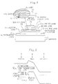
- Figure 8 shows a structure of an NPN heterojunction bipolar transistor having the ⁇ -doped layer provided in the emitter layer according to the present embodiment.
- a high-concentration n-type Si subcollector layer 2 doped with antimony an n-type Si collector layer 3 doped with antimony; a high-concentration p-type SiGe base layer 4 doped with boron; an n-type Si emitter layer 5 doped with antimony; and a high-concentration n-type Si emitter contact layer 6 doped with antimony that have been stacked sequentially on a Si substrate 1 by MBE.
- a collector electrode 20 , a base electrode 21 , and an emitter electrode 22 are disposed on the Si subcollector layer 2 , the SiGe base layer 4 , and the Si emitter contact layer 6 , respectively.
- the thickness of the high-concentration n-type Si subcollector layer 2 is approximately 500 nm and the concentration of antimony (n-type impurity) in the Si subcollector 2 is approximately 2 x 10 19 cm -3 .
- the thickness of the n-type Si collector layer 3 is approximately 650 nm and the concentration of antimony in the Si collector layer 3 is approximately 1 x 10 17 cm -3 .
- the thickness of the high-concentration p-type SiGe base layer 4 is approximately 50 nm and the concentration of boron (p-type impurity) in the SiGe base layer 4 is approximately 1 x 10 19 cm -3 .
- the thickness of the n-type Si emitter layer 5 is approximately 100 nm and the concentration of antimony in the Si emitter layer 5 is approximately 2 x 10 18 cm -3 .
- the thickness of the high-concentration n-type Si emitter contact layer 6 is approximately 50 nm and the concentration of antimony in the Si emitter contact layer 6 is approximately 2 x 10 19 cm -3 .
- a ⁇ -doped Si layer 11 heavily doped with an n-type impurity is provided in a region of the n-type emitter layer 5 adjacent the emitter/base junction portion.
- the thickness of the ⁇ -doped Si layer 11 is approximately 5 nm and the impurity concentration therein is approximately 1 x 10 20 cm -3 .
- the ⁇ -doped Si layer 11 is disposed in the region of the emitter at a distance of approximately 40 nm from the emitter/base junction portion. Antimony is used as the n-type dopant.
- the SiGe base layer 4 has a graded composition base structure in which a Ge composition ratio increases substantially continually in the range of 0% to 30% from a region in contact with the Si emitter layer 5 toward a region in contact with the Si collector layer 3 .
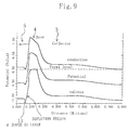
- Figure 9 is a band diagram of the NPN heterojunction bipolar transistor according to the present embodiment, in which the ⁇ -doped Si layer is provided in the emitter layer.
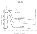
- Figure 10 is a band diagram of the conventional NPN heterojunction bipolar transistor, in which the ⁇ -doped Si layer is not provided in the Si emitter layer.
- the potential barrier height enhanced by the ⁇ -doped Si layer 11 is varied by a carrier concentration in the ⁇ -doped Si layer 11, a carrier concentration in a region of the Si emitter layer 5 on the periphery of the ⁇ -doped Si layer 11 , and an impurity profile in the ⁇ -doped Si layer 11.
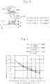
- Figure 11 is a graph showing variations in barrier height plotted against the carrier concentration in the ⁇ -doped Si layer (which is the concentration of an n-type impurity in the present embodiment but is the concentration of a p-type impurity in a PNP heterojunction bipolar transistor) . It is to be noted that Figure 11 is a graph obtained when the carrier concentration in the Si emitter layer is 1 x 10 18 cm -3 . In the present embodiment, the carrier concentration in the Si emitter layer 5 is 2 x 10 18 cm -3 , while the carrier concentration in the ⁇ -doped Si layer 11 is 1 x 10 20 cm -3 , so that the carrier concentration ratio therebetween is 1:50.
- the ⁇ -doped Si layer 11 has enhanced the barrier height by approximately 100 meV, which corresponds to a barrier height when the carrier concentration in the ⁇ -doped Si layer 11 is 5 x 10 19 cm -3 in Figure 11.
- the carrier concentration in the ⁇ -doped Si layer 11 is preferably 1x10 19 cm -3 or higher.
- the increment of the barrier height caused by the ⁇ -doped Si layer 11 is preferably by a factor of 10 or more. It will be understood that the barrier height is higher by 50 meV when the carrier concentration in the ⁇ -doped Si layer 11 is ten times as high as the carrier concentration in the Si emitter layer 5 .
- the carrier concentration in the ⁇ -doped Si layer 11 is preferably more than ten times higher than the carrier concentration in the Si emitter layer 5 .
- the carrier concentration in the SiGe base layer 4 is also possible to desirably reduce the base resistance and suppress a capacitance increase at the PN junction portion.
- Figure 12 is a view showing the relationship (represented by the solid curve) between the current amplification factor ⁇ and a collector current in the NPN heterojunction bipolar transistor in which the ⁇ -doped Si layer 11 is provided in the emitter layer according to the present embodiment and the relationship (represented by the dashed curve) between the current amplification factor ⁇ and a collector current in the conventional NPN heterojunction bipolar transistor in which the ⁇ -doped Si layer is not provided in the emitter layer.
- the current amplification factor ⁇ has been improved in the present embodiment with the provision of the ⁇ -doped Si layer 11 in the Si emitter layer 5 .
- the difference in current amplification factor ⁇ between the two heterojunction bipolar transistors is particularly conspicuous in a region with a large collector current. Since a high current amplification factor ⁇ is obtained in the heterojunction bipolar transistor according to the present embodiment even with such a large collector current, the maximum value f Tmax of the current cutoff frequency is increased by about 25% compared with the maximum value f Tmax in the heterojunction bipolar transistor without a ⁇ -doped Si layer.
- the respective critical film thicknesses for Si 0.8 Ge 0.2 , Si 0.7 Ge 0.3 , and Si 0.6 Ge 0.4 when the underlie is Si are approximately 180 nm, 56 nm, and 25 nm.
- Si 1-x-y Ge x C y In increasing the critical film thickness, it is effective to use Si 1-x-y Ge x C y to compose the base layer.
- the Ge composition By adjusting the Ge composition to 40% or more and adding a slight amount of C (on the order of several percentage) thereto, a strained lattice can be alleviated without greatly varying the magnitude of the band discontinuity value ⁇ Ev of the emitter/base junction, which increases the critical film thickness of the base layer.
- a larger band discontinuity value ⁇ Ev can be obtained without exceeding the critical film thickness.
- the ⁇ -doped Si layer 11 is provided in the Si emitter layer 5 to enhance the effective barrier height.
- the effect of improving the RF characteristics of the HBT having the SiGe graded composition base layer 4 is the same as illustrated in the first embodiment with reference to Figures 5 and 6 .
- HBT heterojunction bipolar transistor
- the provision of the ⁇ -doped Si layer 11 for effectively enhancing the barrier height in the Si emitter layer achieves the same effect as achieved when the band discontinuity value ⁇ Ev of the valence band at the emitter/base junction is substantially increased (see the equation (2)), resulting in an improved current amplification factor ⁇ .
- the provision of the ⁇ -doped Si layer 11 for suppressing reverse injection of holes from the SiGe base layer 4 into the Si emitter layer 5 reduces the current Jp shown in the equation (2) flowing from the base to the emitter and thereby improves the current amplification factor ⁇ .
- the effect is achievable whether the emitter/base junction is a heterojunction or not. Consequently, the same effect can also be achieved in a normal bipolar transistor other than a HBT.
- the Ge composition ratio in the SiGe base layer 4 varies such that the band gap in the SiGe base layer 4 gradually decreases from the region of the SiGe base layer 4 in contact with the Si emitter layer 5 toward the region thereof in contact with the Si collector layer 3 , whereby the current gain cutoff frequency f T is increased.
- the base doping concentration is increased to lower the resistance of the uniform composition base layer in the conventional HBT, the quantity of holes reversely injected is increased so that a sufficient current gain is not obtained.
- the effective barrier height at the heterojunction portion is increased with the provision of the ⁇ -doped Si layer 11 in the HBT according to the present invention
- the effective barrier height is held sufficiently large even when the band discontinuity value of the heterojunction at the emitter/base junction is reduced with the provision of the SiGe graded composition base layer 4 and the base doping concentration is increased, which suppresses reverse injection of holes.
- the heavily doped base layer having a graded composition which has conventionally been unobtainable.
- the base transit time of electrons is reduced and the RF characteristics are improved.
- the thickness of the base layer can be increased. As a result, the base resistance is reduced and the maximum oscillation frequency fmax is increased.
- the fact that a sufficient current gain can be obtained even when the Ge composition ratio is low indicates that a dislocation caused by a thermal budget during the subsequent process step, which presents a problem when a high Ge composition ratio is used, can be suppressed.
- the conventional HBT using the uniform composition base it is required in doping the SiGe base layer with a high-concentration impurity to increase the Ge composition ratio in the SiGe base layer, so that the difference in lattice constant between the emitter layer and the Si base layer is increased disadvantageously to reduce the critical film thickness at which a dislocation is caused by the difference in lattice constant.
- the effective barrier height is enhanced with the provision of the ⁇ -doped Si layer 11 , as in the present embodiment, satisfactory RF characteristics are achieved without increasing the Ge composition ratio in the SiGe base layer 4 .
- the sufficient current gain obtainable with a low Ge composition ratio also achieves the-effect of suppressing the occurrence of a dislocation due to the thermal budget during the subsequent process step, which presents a problem when a high Ge composition ratio is used, i.e., the effect of increasing the thermal budget. Briefly, this achieves the effect of providing the device fabrication process with an increased margin as well as increased device reliability.
- the temperature characteristic of the bipolar transistor can also be improved. Specifically, since the distribution of hole concentrations in the valence band of the SiGe layer 4 shifts downwardly at an increased temperature, the current amplification factor ⁇ of the bipolar transistor exhibits a tendency to lower as the temperature T increases. The tendency is particularly conspicuous when the band discontinuity value ⁇ Ev is low.
- the bipolar transistor according to the present invention provides a high current amplification factor ⁇ even at a high temperature owing to the function of suppressing reverse injection of holes performed by the ⁇ -doped Si layer 11 , as represented by the line 3 in Figure 7(b) .
- the current gain and RF characteristics of the heterojunction bipolar transistor can be improved.
- the whole ⁇ -doped Si layer 11 is preferably disposed externally of a depletion region formed between the emitter and the base at a working voltage and the ⁇ -doped Si layer 11 is preferably adjacent to the depletion region.
- the ⁇ -doped Si layer 11 in the Si emitter layer 5 is at a distance shorter than the diffusion length of hole from the SiGe base layer 4 .
- the present embodiment has described the improved characteristics of the heterojunction bipolar transistor as a single element, it will easily be appreciated that the HBT according to the present invention may also be used for the bipolar part of a BiCMOS device in which the bipolar transistor and a MOS transistor have been integrated.
- the present embodiment has described the NPN SiGe HBT by way of example, it will easily be appreciated that the present invention is also applicable to a PNP bipolar transistor. Alternatively, the present invention may also be applied to a normal homojunction bipolar transistor other than the HBT and to a heterojunction bipolar transistor having a multi-level structure consisting of III-V compound semiconductor layers of GaAs, AlGaAs, and the like, as stated previously.
- Figure 13 is a cross-sectional view showing a structure of an NPN heterojunction bipolar transistor having a multi-quantum barrier composed of a Si/SiGe superlattice provided in the collector layer according to the present embodiment.
- a high-concentration n-type Si subcollector layer 2 doped with arsenic there are provided: a high-concentration n-type Si subcollector layer 2 doped with arsenic; an n -type Si collector layer 3 doped with arsenic; a high-concentration p-type SiGe base layer 4 doped with boron; an n-type Si emitter layer 5 doped with arsenic; and a high-concentration n-type Si emitter contact layer 6 doped with arsenic that have been stacked sequentially on a Si substrate 1 .
- a collector electrode 20 , a base electrode 21 , and an emitter electrode 22 are disposed on the Si subcollector layer 2 , the SiGe base layer 4 , and the Si
- the thickness of the high-concentration n-type Si subcollector layer 2 is approximately 500 nm and the concentration of arsenic (n-type impurity) in the Si subcollector 2 is approximately 2 x 10 19 cm -3 .
- the thickness of the n-type Si collector layer 3 is approximately 650 nm and the concentration of the Si collector layer 3 is approximately 1 x 10 17 cm -3 .
- the thickness of the high-concentration p-type SiGe base layer 4 is approximately 50 nm and the concentration of boron (p-type impurity) in the SiGe base layer 4 is approximately 1 x 10 19 cm -3 .
- the thickness of the n-type Si emitter layer 5 is approximately 100 nm and the concentration of arsenic in the Si emitter layer 5 is approximately 2 x 10 18 cm -3 .
- the thickness of the high-concentration n-type Si emitter contact layer 6 is approximately 50 nm and the concentration of arsenic in the Si emitter contact layer 6 is approximately 2 x 10 19 cm -3 .
- a MQB layer 12 as a multi-quantum barrier portion having a superlattice structure composed of extremely thin Si and SiGe that have been alternately stacked is provided in a region of the Si collector layer 3 adjacent the collector/base junction portion.
- the MQB layer 12 has such a structure that the compositions and film thicknesses thereof have been adjusted to reflect an incident wave of holes injected from the SiGe base layer 4 into the Si collector layer 3 and provide a phase in which the incident wave and a reflected wave intensify each other.
- the MQB layer 12 has a multilayer structure consisting of well layers 12a each composed of a SiGe layer with a thickness of L1 and barrier layers 12b each composed of a Si layer with a thickness of L2.
- the respective thicknesses and compositions of the well layers 12a and the barrier layers 12b are determined to satisfy the relationship represented by the following equation (3), similarly to the first embodiment.
- the MQB layer 12 is composed of a superlattice layer constructed of five pairs of the barrier layers 12b each formed of Si having a thickness of 1.5 nm and the well layers 12a each formed of Si 0.8 Ge 0.2 having a thickness of 1.5 nm.
- an effective barrier height enhanced by the MQB layer 12 is approximately 130 meV.
- the SiGe base layer 4 has a graded composition base structure in which a Ge composition ratio increases substantially continually from 0% to 20% from a region in contact with the Si emitter layer 5 toward a region in contact with the Si collector layer 3 .
- the barrier height sensed by holes in the SiGe layer 4 is 280 meV, which is the sum of 150 meV corresponding to the amount of valence band offset occurring at the base/collector heterojunction composed of Si/Si 0.8 Ge 0.2 and 130 meV corresponding to the effectively enhanced barrier height of the MQB layer 12 . This achieves a sufficient reduction in the minority carriers injected from the SiGe base layer 4 and accumulated in the Si collector layer 4 .
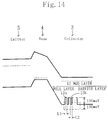
- Figure 14 is a band diagram of the NPN heterojunction bipolar -transistor having the multi-quantum barrier layer composed of the Si/SiGe superlattice and provided in the Si collector layer 3 according to the present embodiment.
- the multi-quantum barrier layer consisting of the five pairs of Si barrier layers 12b and Si 0.8 Ge 0.2 well layers 12a is provided in a region of the Si collector layer 3 adjacent the collector/base junction.
- a potential barrier indicated by the broken lines in Figure 14 is formed due to the existence of the MQB layer 12.
- the potential barrier operates to reflect holes likely to flow from the SiGe base layer 4 into the Si collector layer 3 , which has enhanced an effective height sensed by the holes likely to flow from the SiGe base layer 4 by approximately 130 meV.
- the enhanced effective barrier height suppresses injection of the holes into the Si collector layer 3 so that the quantity of minority carriers accumulated in the Si collector layer 3 is reduced and the operating speed is increased.
- the model for calculating the barrier height ⁇ Ue enhanced by the MQB layer 12 provided in the collector is similar to the model for calculating the barrier height ⁇ Ue in the case where the MQB layer is provided in the emitter according to the first embodiment, which is shown in Figure 3.
- the respective band discontinuity values ⁇ Ev of the valence bands at the individual heterojunctions between the well layers 12a and the barrier layers 12b that have been calculated for the three structures of Si/Si 0.8 Ge 0.2 , Si/Si 0.7 Ge 0.3 , and Si/Si 0.6 Ge 0.4 are 150 meV, 225 meV, and 300 meV. It is to be noted that, since each of the well layers 12a and barrier layers 12b has a thickness of 1.5 nm in the present embodiment, the values obtained in the present embodiment are different from the values of the corresponding parts shown in Figure 3.
- the increased Ge composition ratio may cause a dislocation depending on the critical film thickness of SiGe.
- the respective critical film thicknesses for Si 0.8 Ge 0.2 , Si 0.7 Ge 0.3 , and Si 0.6 Ge 0.4 when the underlie is Si are approximately 180 nm, 56 nm, and 25 nm.
- Si 1-x-y Ge x C y and Si to compose the well layers 12a and barrier layers 12b of the MQB layer 12 , respectively.
- a strained lattice can be alleviated without greatly varying the magnitude of the band discontinuity value ⁇ Ev at the collector/base junction, which increases the critical film thickness of the well layer 12a.
- the MQB layer 12 in the region of the Si collector layer 3 adjacent the base/collector junction of the heterojunction bipolar transistor, it becomes possible to effectively enhance the height of the heterojunction barrier at the base/collector heterojunction and thereby suppress injection of minority carriers from the SiGe base layer 4 into the Si collector layer 3 . As a result, the quantity of minority carriers accumulated in the Si collector layer 3 is reduced and the operating speed of the bipolar transistor can be increased.
- the present embodiment has described the improved characteristics of the heterojunction bipolar transistor as a single element, it will easily be appreciated that the HBT according to the present invention may also be used for the bipolar part of a BiCMOS device in which the bipolar transistor and a MOS transistor have been integrated.
- Figure 15 is a cross-sectional view of an I 2 L element comprising a Si/SiGe heterojunction bipolar transistor having a MQB layer provided in a collector layer as shown in the third embodiment.
- Figure 16 is an electric circuit diagram showing a circuit equivalent to the I 2 L element.
- the I 2 L element comprises: an n + -type semiconductor region 51 ; an n-type Si common diffusion layer 52 disposed on the semiconductor region 51 to function as the base layer of a PNP bipolar transistor and as the emitter layer of an NPN bipolar transistor; a Si emitter layer 53 and a Si collector 54 of the PNP bipolar transistor formed by introducing a p-type impurity into the Si common diffusion layer 52 ; a p-type SiGe base layer 55 of the I 2 L element disposed on the Si common diffusion layer 52; two n-type Si collector layers 56a and 56b of the NPN bipolar transistor disposed on the SiGe base layer 55 ; an insulating layer 57 covering the entire substrate; two collector electrodes 70a and 70b of the NPN bipolar transistor for contact with the Si collector layers 56a and 56b through the insulating layer 57 ; a base electrode 71 of the I
- the SiGe base layer 55 of the I 2 L element functions as the base layer of the NPN bipolar transistor and as the collector contact layer of the PNP bipolar transistor.
- the I 2 L element is structured such that a current for driving the PNP transistor is injected into the injection electrode 72, an input signal to the I 2 L element is inputted to the base electrode 71, and an output signal from the I 2 L element is obtained from each of the collector electrodes 70a and 70b connected to a power source voltage via a circuit (not shown).
- the arrows shown in Figure 15 represent respective current flows in the PNP and NPN bipolar transistors.
- the concentration of arsenic (n-type impurity) in each of the Si collector layers 56a and 56b is approximately 1 x 10 17 cm -3 .
- a contact layer doped with arsenic at a high concentration (approximately 1 x 10 20 cm -3 ), though it is not shown.
- the concentration of boron (p-type impurity) in the SiGe base layer 55 is approximately 2 x 10 18 cm -3 .
- the concentration of boron in the Si emitter layer 53 is approximately 1 x 10 19 cm -3 .
- the concentration of boron in the Si collector layer 54 is approximately 1 x 10 19 cm -3 .
- the concentration of phosphorus in the Si common diffusion layer 52 is approximately 1 x 10 18 cm -3 .
- the I 2 L element functions as a NOT circuit (inverter).
- the I 2 L element according to the present embodiment is characterized in that the same MQB layers 60a and 60b as formed in the first embodiment are formed in the two Si collector layers 56a and 56b , respectively.
- Such an I 2 L element performs the same function as performed by an inverter composed of the PFET and NFET of a CMOS device. Since the I 2 L element does not require an isolation film as required by the CMOS device, it has the advantage of suitability for higher integration. However, a conventional I 2 L element has the drawback of an elongated time required for ON/OFF switching due to minority carriers accumulated in the collector layer of the NPN bipolar transistor. For this reason, the I 2 L element is not frequently used in a semiconductor integrated circuit.
- the structure of the I 2 L element according to the present embodiment has the MQB layers 60a and 60b provided in the Si collector layers 56a and 56b , respectively, for preventing injection of holes from the base, it is free from the elongated ON/OFF switching time due to holes (minority carriers) accumulated in the Si collector layers 56a and 56b and performs a high-speed operation intrinsic to a bipolar transistor.
- the I 2 L element has the advantages of suitability for higher integration and a high-speed operating property, which allows the use of the I 2 L element as an inverter in a Si heterojunction device.
- power consumption is satisfactorily low compared with the power consumption of a MOS device.
- the I 2 L element according to the present embodiment further has the following structural advantages.
- the NPN bipolar transistor on the output side of the I 2 L element has a so-called collector top structure in which the Si collector layers 56a and 56b are disposed above the SiGe base layer 55 .
- the collector top structure is suitable for the provision of the MQB layers 60a and 60b formed by epitaxial growth.
- the I 2 L element has the collector top structure in which the collector layer is formed above the base layer because of a plurality of collector outputs, while a normal Si/SiGe HBT generally has an emitter top structure in which an emitter layer is formed above a SiGe base layer formed by epitaxial growth.
- the emitter and base regions of the NPN bipolar transistor also serve as the base and collector regions of the PNP bipolar transistor as a constant current source, so that the base and collector layers of the NPN transistor are eventually formed by epitaxial growth above the emitter layer.
- the I 2 L element having the MQB layers provided in a region of the collector adjacent the base/collector junction portion of the HBT has an easy-to-fabricate structure.
- the present embodiment has described the I 2 L element using the NPN SiGe HBT, it is also possible to compose the I 2 L element by using a PNP SiGe HBT.
- the I 2 L element according to the present embodiment may be a heterojunction bipolar transistor having a multi-level structure consisting of III-V compound semiconductor layers of GaAs, AlGaAs, and the like.
- the present embodiment has the two collector layers, it may also have a single collector layer or three or more collector layers.
- the semiconductor device has a bipolar transistor formation region and a diode formation region.
- the bipolar transistor formation region and the diode formation region have common members, except for electrodes, which are formed by common process steps.
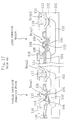
- a Si collector layer 103 there are provided: a Si collector layer 103; a p-type SiGe base layer 104 formed on the Si collector layer 103 ; an n + -type Si emitter layer 105 formed on the SiGe base layer 104 ; an emitter withdrawn electrode 106 composed of polysilicon for contact with the Si emitter layer 105 ; and a MQB layer 110 formed on a region of the Si collector layer 103 underlying a first exposed region Rexp1 , each of which is located in an active region composed of the first and second exposure regions Rexp1 and Rexp2 of the Si substrate 101 surrounded by LOCOS films 102 and of the internal region of the substrate interposed between the exposed regions Rexp1 and Rexp2 .
- a first Si single-crystal film including the Si collector layer 103 is formed by epitaxial growth over the first exposed region Rexp1 and the surrounding LOCOS films, which is thoroughly provided with a superlattice multi-layer structure common to the MQB layer 110 .
- a p-type impurity has been introduced into the first Si single-crystal film except for the region thereof immediately under the emitter withdrawn electrode 106 by ion implantation using the emitter withdrawn electrode 106 as a mask.
- the SiGe base layer 104 is formed over the first Si single-crystal film and a second Si single-crystal film is further formed by epitaxial growth over the SiGe base layer 104 .
- the second Si single-crystal film except for the region thereof immediately under the emitter withdrawn electrode 106 forms a silicide layer 108 , while the region immediately under the emitter withdrawn electrode 106 forms a Si cap layer 109 .
- the foregoing Si emitter layer 105 has been formed by introducing, by diffusion, a high-concentration n-type impurity into the Si cap layer 109 from the emitter withdrawn electrode 106 .
- a collector withdrawn electrode 111 composed of polysilicon for contact with the Si collector layer 103 is formed over the second exposed region Rexp2 and the surrounding LOCOS films 102 .
- An insulating film 112 composed of a silicon oxide film is formed on the substrate.
- the concentration of arsenic (n-type impurity) in the Si collector layer 103 is approximately 1 x 10 17 cm -3 .
- the thickness of the SiGe base layer 104 is approximately 50 nm and the concentration of boron (p-type impurity) in the SiGe base layer 104 is approximately 1 x 10 19 cm -3 .
- the thickness of the Si cap layer 109 is approximately 100 nm and the concentration of arsenic in the Si emitter layer 105 of the Si cap layer 109 is approximately 2 x 10 18 cm -3 .
- the present embodiment is characterized in that the diode has no electrode equivalent to the emitter electrode, while the NPN bipolar transistor has an A1 emitter electrode 115 connected to the emitter withdrawn electrode 106, an A1 base electrode 116 connected to the silicide layer provided on the Si base layer 104, and an A1 collector electrode 117, each of which is formed on the insulating layer 112 .
- the diode according to the present embodiment has only the anode and the cathode connected to the base and to the collector, respectively, without an electrode connected to the emitter, while having the same emitter, base, and collector structures as the NPN bipolar transistor.
- the semiconductor device comprises the diode having a heterojunction in addition to the heterojunction bipolar transistor exerting the same effect as exerted in the third embodiment.
- the diode also, there is provided a MQB layer in a region of the Si collector layer 103 connected to the cathode electrode 119 adjacent the junction portion between the Si collector layer 103 and the SiGe base layer 104 , so that the operating speed is increased by suppressing the accumulation of holes.
- the present embodiment has described the NPN SiGe HBT by way of example, it will easily be appreciated that the present invention is also applicable to the PNP bipolar transistor. As stated previously, the present invention is also applicable to a normal homojunction bipolar transistor other than a HBT or to a heterojunction bipolar transistor having a multi-layer structure consisting of III-V compound semiconductor layers of GaAs, AlGaAs, and the like.
Landscapes
- Bipolar Transistors (AREA)
Applications Claiming Priority (7)
| Application Number | Priority Date | Filing Date | Title |
|---|---|---|---|
| JP3875898 | 1998-02-20 | ||
| JP03875898A JP3305250B2 (ja) | 1998-02-20 | 1998-02-20 | バイポーラトランジスタ |
| JP15470098 | 1998-06-03 | ||
| JP15468998A JP3352629B2 (ja) | 1998-06-03 | 1998-06-03 | バイポーラトランジスタ |
| JP15468998 | 1998-06-03 | ||
| JP15470098A JP3295373B2 (ja) | 1998-06-03 | 1998-06-03 | 半導体装置 |
| EP99103330A EP0938140B1 (de) | 1998-02-20 | 1999-02-19 | Halbleiterbauelement mit Bipolartransistor |
Related Parent Applications (1)
| Application Number | Title | Priority Date | Filing Date |
|---|---|---|---|
| EP99103330A Division EP0938140B1 (de) | 1998-02-20 | 1999-02-19 | Halbleiterbauelement mit Bipolartransistor |
Publications (2)
| Publication Number | Publication Date |
|---|---|
| EP1178537A2 true EP1178537A2 (de) | 2002-02-06 |
| EP1178537A3 EP1178537A3 (de) | 2004-09-29 |
Family
ID=27289932
Family Applications (2)
| Application Number | Title | Priority Date | Filing Date |
|---|---|---|---|
| EP01123874A Withdrawn EP1178537A3 (de) | 1998-02-20 | 1999-02-19 | Bipolartransistor und Halbleiterbauelement |
| EP99103330A Expired - Lifetime EP0938140B1 (de) | 1998-02-20 | 1999-02-19 | Halbleiterbauelement mit Bipolartransistor |
Family Applications After (1)
| Application Number | Title | Priority Date | Filing Date |
|---|---|---|---|
| EP99103330A Expired - Lifetime EP0938140B1 (de) | 1998-02-20 | 1999-02-19 | Halbleiterbauelement mit Bipolartransistor |
Country Status (4)
| Country | Link |
|---|---|
| EP (2) | EP1178537A3 (de) |
| CN (1) | CN1226750A (de) |
| DE (1) | DE69935024T2 (de) |
| TW (1) | TW412808B (de) |
Cited By (1)
| Publication number | Priority date | Publication date | Assignee | Title |
|---|---|---|---|---|
| EP2202784A2 (de) | 2008-12-29 | 2010-06-30 | Imec | Herstellungsverfahren für einen Übergang |
Families Citing this family (11)
| Publication number | Priority date | Publication date | Assignee | Title |
|---|---|---|---|---|
| DE19944925B4 (de) * | 1999-09-13 | 2010-11-25 | Ihp Gmbh - Innovations For High Performance Microelectronics / Leibniz-Institut Für Innovative Mikroelektronik | Schichtstruktur für bipolare Transistoren und Verfahren zu deren Herstellung |
| JP3528756B2 (ja) * | 2000-05-12 | 2004-05-24 | 松下電器産業株式会社 | 半導体装置 |
| US6426265B1 (en) * | 2001-01-30 | 2002-07-30 | International Business Machines Corporation | Incorporation of carbon in silicon/silicon germanium epitaxial layer to enhance yield for Si-Ge bipolar technology |
| CN106169498B (zh) * | 2016-07-30 | 2019-03-05 | 北京工业大学 | 高热稳定性超结应变Si/SiGe异质结双极晶体管 |
| JP2018101652A (ja) * | 2016-12-19 | 2018-06-28 | 株式会社村田製作所 | バイポーラトランジスタ及びその製造方法 |
| JP2019075424A (ja) * | 2017-10-13 | 2019-05-16 | 株式会社村田製作所 | ヘテロ接合バイポーラトランジスタ |
| TWI643337B (zh) * | 2017-10-17 | 2018-12-01 | 全新光電科技股份有限公司 | 具有能隙漸變的電洞阻隔層之異質接面雙極性電晶體結構 |
| CN109686788B (zh) * | 2018-11-20 | 2020-12-29 | 电子科技大学 | 一种具有载流子存储层的槽栅igbt器件 |
| US11404540B2 (en) * | 2019-10-01 | 2022-08-02 | Analog Devices International Unlimited Company | Bipolar junction transistor, and a method of forming a collector for a bipolar junction transistor |
| US11355585B2 (en) | 2019-10-01 | 2022-06-07 | Analog Devices International Unlimited Company | Bipolar junction transistor, and a method of forming a charge control structure for a bipolar junction transistor |
| US11563084B2 (en) | 2019-10-01 | 2023-01-24 | Analog Devices International Unlimited Company | Bipolar junction transistor, and a method of forming an emitter for a bipolar junction transistor |
Family Cites Families (5)
| Publication number | Priority date | Publication date | Assignee | Title |
|---|---|---|---|---|
| DE4039103A1 (de) * | 1990-03-27 | 1991-10-02 | Daimler Benz Ag | Bipolare halbleiteranordnung und verfahren zu deren herstellung |
| GB2288691B (en) * | 1991-10-02 | 1996-06-12 | Mitsubishi Electric Corp | Bipolar semiconductor device and production method therfor |
| JP2731089B2 (ja) * | 1991-10-02 | 1998-03-25 | 三菱電機株式会社 | 高速動作半導体装置およびその製造方法 |
| US5426316A (en) * | 1992-12-21 | 1995-06-20 | International Business Machines Corporation | Triple heterojunction bipolar transistor |
| JPH09283533A (ja) * | 1996-04-15 | 1997-10-31 | Matsushita Electric Ind Co Ltd | ヘテロ接合バイポーラトランジスタ |
-
1999
- 1999-02-19 EP EP01123874A patent/EP1178537A3/de not_active Withdrawn
- 1999-02-19 DE DE69935024T patent/DE69935024T2/de not_active Expired - Fee Related
- 1999-02-19 EP EP99103330A patent/EP0938140B1/de not_active Expired - Lifetime
- 1999-02-20 TW TW088102479A patent/TW412808B/zh not_active IP Right Cessation
- 1999-02-23 CN CN99100820.0A patent/CN1226750A/zh active Pending
Cited By (2)
| Publication number | Priority date | Publication date | Assignee | Title |
|---|---|---|---|---|
| EP2202784A2 (de) | 2008-12-29 | 2010-06-30 | Imec | Herstellungsverfahren für einen Übergang |
| EP2202784A3 (de) * | 2008-12-29 | 2010-12-08 | Imec | Herstellungsverfahren für einen Übergang |
Also Published As
| Publication number | Publication date |
|---|---|
| EP0938140A2 (de) | 1999-08-25 |
| TW412808B (en) | 2000-11-21 |
| EP0938140A3 (de) | 1999-11-24 |
| DE69935024D1 (de) | 2007-03-22 |
| EP1178537A3 (de) | 2004-09-29 |
| EP0938140B1 (de) | 2007-01-31 |
| DE69935024T2 (de) | 2007-05-24 |
| CN1226750A (zh) | 1999-08-25 |
Similar Documents
| Publication | Publication Date | Title |
|---|---|---|
| US6737684B1 (en) | Bipolar transistor and semiconductor device | |
| US6759697B2 (en) | Heterojunction bipolar transistor | |
| JP3573737B2 (ja) | ヘテロ接合バイポーラ・トランジスタおよび半導体集積回路 | |
| US5440152A (en) | Heterojunction bipolar transistor having particular Ge distributions and gradients | |
| US6821870B2 (en) | Heterojunction bipolar transistor and method for fabricating the same | |
| EP0541971B1 (de) | Heteroübergang-Bipolartransistor mit Emitter aus gradiertem Bandabstand-Monokristall | |
| EP0504925B1 (de) | Heteroübergangsbauelement mit einer mehrschichtigen Basis | |
| US20050051798A1 (en) | Silicon germanium heterojunction bipolar transistor with carbon incorporation | |
| EP0938140B1 (de) | Halbleiterbauelement mit Bipolartransistor | |
| EP0657942A2 (de) | Lateraler Bipolartransistor | |
| US4924283A (en) | Heterojunction bipolar transistor and process for fabricating same | |
| US5336909A (en) | Bipolar transistor with an improved collector structure | |
| EP0292568B1 (de) | Bipolartransistor mit heteroübergang | |
| US5272357A (en) | Semiconductor device and electronic device by use of the semiconductor | |
| JP2001338930A (ja) | 半導体装置および半導体製造方法 | |
| EP1662557B1 (de) | Bipolartransistor mit heteroübergang | |
| JP3463776B2 (ja) | ヘテロ接合半導体デバイス | |
| JP5160071B2 (ja) | ヘテロ接合バイポーラトランジスタ | |
| WO1987000692A1 (en) | Semiconductor device | |
| JP3295373B2 (ja) | 半導体装置 | |
| JP2011003840A (ja) | ヘテロ接合バイポーラトランジスタ | |
| JP3352629B2 (ja) | バイポーラトランジスタ | |
| JPH08288300A (ja) | ヘテロ接合バイポーラトランジスタ | |
| JP2915058B2 (ja) | 半導体装置および該装置を用いた光電変換装置 | |
| JP2010287603A (ja) | 化合物半導体素子及びその製造方法 |
Legal Events
| Date | Code | Title | Description |
|---|---|---|---|
| PUAI | Public reference made under article 153(3) epc to a published international application that has entered the european phase |
Free format text: ORIGINAL CODE: 0009012 |
|
| AC | Divisional application: reference to earlier application |
Ref document number: 938140 Country of ref document: EP |
|
| AK | Designated contracting states |
Kind code of ref document: A2 Designated state(s): DE FR GB NL |
|
| PUAL | Search report despatched |
Free format text: ORIGINAL CODE: 0009013 |
|
| AK | Designated contracting states |
Kind code of ref document: A3 Designated state(s): DE FR GB NL |
|
| 17P | Request for examination filed |
Effective date: 20050119 |
|
| AKX | Designation fees paid |
Designated state(s): DE FR GB NL |
|
| RAP1 | Party data changed (applicant data changed or rights of an application transferred) |
Owner name: PANASONIC CORPORATION |
|
| STAA | Information on the status of an ep patent application or granted ep patent |
Free format text: STATUS: THE APPLICATION HAS BEEN WITHDRAWN |
|
| 18W | Application withdrawn |
Effective date: 20090916 |