EP1179218B1 - Dispositif semi-conducteur et procede de fabrication associe - Google Patents
Dispositif semi-conducteur et procede de fabrication associe Download PDFInfo
- Publication number
- EP1179218B1 EP1179218B1 EP01911561A EP01911561A EP1179218B1 EP 1179218 B1 EP1179218 B1 EP 1179218B1 EP 01911561 A EP01911561 A EP 01911561A EP 01911561 A EP01911561 A EP 01911561A EP 1179218 B1 EP1179218 B1 EP 1179218B1
- Authority
- EP
- European Patent Office
- Prior art keywords
- gate
- recess
- semiconductor body
- semiconductor device
- silicon oxide
- Prior art date
- Legal status (The legal status is an assumption and is not a legal conclusion. Google has not performed a legal analysis and makes no representation as to the accuracy of the status listed.)
- Expired - Lifetime
Links
Images


Classifications
-
- H—ELECTRICITY
- H10—SEMICONDUCTOR DEVICES; ELECTRIC SOLID-STATE DEVICES NOT OTHERWISE PROVIDED FOR
- H10P—GENERIC PROCESSES OR APPARATUS FOR THE MANUFACTURE OR TREATMENT OF DEVICES COVERED BY CLASS H10
- H10P10/00—Bonding of wafers, substrates or parts of devices
-
- H—ELECTRICITY
- H10—SEMICONDUCTOR DEVICES; ELECTRIC SOLID-STATE DEVICES NOT OTHERWISE PROVIDED FOR
- H10D—INORGANIC ELECTRIC SEMICONDUCTOR DEVICES
- H10D30/00—Field-effect transistors [FET]
- H10D30/60—Insulated-gate field-effect transistors [IGFET]
- H10D30/67—Thin-film transistors [TFT]
- H10D30/6729—Thin-film transistors [TFT] characterised by the electrodes
- H10D30/673—Thin-film transistors [TFT] characterised by the electrodes characterised by the shapes, relative sizes or dispositions of the gate electrodes
- H10D30/6733—Multi-gate TFTs
- H10D30/6734—Multi-gate TFTs having gate electrodes arranged on both top and bottom sides of the channel, e.g. dual-gate TFTs
-
- H—ELECTRICITY
- H10—SEMICONDUCTOR DEVICES; ELECTRIC SOLID-STATE DEVICES NOT OTHERWISE PROVIDED FOR
- H10D—INORGANIC ELECTRIC SEMICONDUCTOR DEVICES
- H10D64/00—Electrodes of devices having potential barriers
- H10D64/01—Manufacture or treatment
- H10D64/017—Manufacture or treatment using dummy gates in processes wherein at least parts of the final gates are self-aligned to the dummy gates, i.e. replacement gate processes
Definitions
- the invention relates to a semiconductor device with a silicon semiconductor body having a first surface and a second surface facing away from the first, provided with a field effect transistor comprising a source, a drain, an interposed channel, and a first gate arranged opposite the channel on the first surface, said gate having a dimension along said first surface, and provided with a second gate provided on the second surface opposite the first gate.
- the invention also relates to a method of manufacturing a semiconductor device with a silicon semiconductor body having a first surface and a second surface facing away from the first, and provided with a field effect transistor comprising a source, a drain, an interposed channel and a first gate provided on the first surface opposite the channel, and a second gate of a second gate material provided on the second surface opposite the channel.
- Such a semiconductor device is known from JP-A-04 307972 .
- the known semiconductor device is provided with a second gate.
- a second gate is the suppression of short-channel effects in field effect transistors (FETs) with a comparatively short first gate. If the first gate is comparatively short, the channel between source and drain is comparatively short. Short-channel effects are effects in a field effect transistor having a short channel which are caused by the extension of the depletion region of the drain into the channel under the influence of a voltage on the drain. To suppress these short-channel effects, a second gate is present, and this second gate has to be accurately positioned opposite the channel of the FET. Field effect transistors are made increasingly smaller, with a shorter first gate and accordingly a shorter channel, especially for increasing the speed and the current-carrying power. There is a worldwide demand for improving the performance and reliability of FETs through the suppression of short-channel effects.
- the second gate is manufactured by lithography and etching. It is practically impossible, however, to carry out lithographic operations on the second surface in locations which are accurately aligned with respect to the first surface.
- a major disadvantage of the known device is that products from one and the same batch have diverging properties as a result of the method by which they were manufactured.
- the position of the second gate is not accurately defined with respect to the first gate of the FET and varies from one device to the next in devices belonging to one batch.
- Another disadvantage is that the dimension of the second gate also varies.
- a double gate FET with a gate formed in a recess of a semiconductor body is known from US-A-5,736,435 (corresponding to the preamble of claim 1).
- the invention also has for its object to provide a method of manufacturing the device described in the opening paragraph which positions the second gate accurately with respect to the first gate.
- the semiconductor body has a recess with a depth in the second surface, which recess is concentric with a substantially perpendicular projection of the first gate, and in which recess the second gate is present.
- the semiconductor body has a recess in the second surface which is concentric with a substantially perpendicular projection of the first gate, the second gate being present in said recess, the second gate is closer to the channel in the semiconductor body than if no such recess were present in the semiconductor body.
- the distance from the second gate to the channel is shorter because the second gate lies substantially perpendicularly below the first gate, compared with the situation in which the second gate is laterally shifted.
- the dimension of the second gate may differ from that of the first gate, but in a favorable embodiment the second gate has a dimension along the second surface, averaged over the depth of the recess, which corresponds substantially to at most the dimension of the first gate.
- Overlap capacitances between portions of the second gate laterally of a perpendicular projection of the first gate and the semiconductor body are substantially minimized.
- the speed of the transistor is improved thereby.
- the location of the second gate is accordingly limited, and the dimension of the second gate is accordingly accurately defined with respect to the first gate of the FET, so that the properties of the semiconductor device are laid down within narrow limits.
- the recess may be filled only partly, but it is favorable when the recess is completely filled by the second gate.
- the material from which the second gate is made may be comparatively strongly doped polycrystalline silicon or a metal.
- a closed layer of gate material in the recess for example a layer which covers the bottom wall of the recess, is sufficient already for a satisfactory operation of the second gate. To reduce the resistance of the second gate, it is favorable when the recess is completely filled with the second gate. It is alternatively possible, however, for the second gate to cover only a portion of the bottom wall and to be smaller than the first gate.
- a gate dielectric may be present between the first gate and the first surface, so that the field effect transistor operates as a metal-insulator-semiconductor field effect transistor (MISFET).
- MISFET metal-insulator-semiconductor field effect transistor
- a field effect transistor with a gate dielectric has a lower gate leakage current than a field effect transistor without a gate dielectric.
- a gate dielectric may be present in the recess, between the second gate and the semiconductor body, so that the second gate is capacitively coupled to the semiconductor body.
- a major advantage of a capacitive coupling is a low gate leakage current.
- the control of the second gate over the channel is better in proportion as the gate dielectric is thinner.
- the semiconductor body lies on an oxide layer and, for example, a silicon substrate during the manufacture of the semiconductor device. It is favorable when the semiconductor body has a lowest possible parasitic capacitive coupling to the substrate. If a second substrate is present against the first gate and the first surface of the semiconductor body, the device will have an additional sturdiness for the purpose of removing the original silicon substrate and the oxide layer. If the second substrate has a dielectric constant which is lower than the effective dielectric constant of the oxide layer with the silicon substrate, the parasitic coupling between the semiconductor body and the second substrate will be reduced.
- the object of the invention as regards the method is realized - according to the invention - in that the semiconductor body with the first gate on the first surface and a silicon oxide layer on the second surface is implanted with dopant ions in a direction substantially perpendicular to the first surface and through the first surface so as to form an implanted region behind the first gate in the silicon semiconductor body and an implanted zone in the silicon oxide layer around said region, whereupon silicon oxide is formed by dopant-enhanced oxidation in the implanted region and the silicon oxide in said region and the silicon oxide layer are removed, such that a recess is created in the second surface at the area of said region, and the second gate material is provided in said recess, from which material the second gate is formed.
- the method according to the invention is essentially based on the recognition that the oxidation speed depends on the local doping level.
- Dopant ions for example Sb, As, P, or B, are implanted in a direction substantially perpendicular to the first surface both through the first gate and through the first surface.
- the dopant ions lose part of their energy at the area of the first gate owing to collision processes in the first gate, so that the implanted region lies behind the gate in the semiconductor, whereas this energy loss does not occur in the zone around the first gate, and the dopant ions are implanted more deeply, i.e. in the oxide layer.
- the implanted region in the semiconductor body lies substantially perpendicularly behind the first gate and is comparatively strongly doped.
- the implanted region has a steeper concentration profile of the dopant ions at the edges if implantation took place with heavy ions, such as arsenic and antimony, than if implantation took place with lighter ions, such as boron and phosphorus. Since the oxidation speed depends on the doping level, the oxide layer grows faster at the area behind the first gate in the comparatively strongly doped region of the silicon semiconductor body than in the comparatively weakly doped surrounding silicon zone during the oxidation process. This causes a recess of a certain depth which is concentric with a substantially perpendicular projection of the first gate in the second surface of the semiconductor body at the area of the implanted region. During the oxidation, the dopant ions implanted into the zone of the oxide layer remain in the oxide layer.
- the entire product is turned upside down.
- the silicon oxide layer with the silicon oxide formed during the dopant-enhanced oxidation is removed.
- the second gate may be provided in various ways.
- the second gate may be made in that a layer of a second gate material, for example polycrystalline silicon or metal, is deposited on the second surface with the recess and subsequently the layer laterally of the recess is removed from the second surface, for example by polishing.
- a second gate material for example polycrystalline silicon or metal
- the second gate material remains in the recess at the area of the recess, so that at least the bottom wall of the recess is covered, or the entire recess is filled up with the second gate, depending on the thickness of the layer and the depth of the recess.
- a second gate is made in this manner which is substantially perpendicularly below the first gate and has substantially the same dimensions as the first gate.
- the second gate may alternatively be made as follows.
- a layer of second gate material for example polycrystalline silicon or metal, is deposited on the second surface with the recess.
- a photoresist layer is provided over the gate material.
- the photoresist is a negative resist.
- the photoresist layer is exposed to light.
- the light is reflected by the second gate material.
- the photoresist situated above the center of the recess is exposed most strongly.
- the pattern of the second gate in statu nascendi remains in the resist. This pattern in the resist lies accurately centered with respect to the center of the recess and serves as a mask in the subsequent etching of the second gate material.
- the resist is removed, and the second gate has been completed.
- a gate dielectric may be provided in the recess before the second gate material is provided.
- the gate dielectric in the recess of the second surface between the second gate and the second surface serves to realize a low gate leakage current.
- the semiconductor device may comprise a CMOS logic circuit, memories, or a combination of the two.
- logic applications the voltage gain and the depletion mode operation are important, whereas it is important in memory applications to be able to modulate the current over different orders of magnitude.
- An additional advantage is that the second gate may be used both in CMOS logic and in memories. It is possible to combine logic with memory applications, with the possibility of making the second gate in the recess in one process simultaneously for all transistors of the semiconductor device.
- the width of the inversion channel is so small that it is in fact a quantum well with a two-dimensional electron gas. This confinement renders it possible to make a device based on Coulomb blockade, single-electron effects, or quantum effects such as charge quantization.
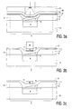
- the semiconductor device of Fig. 1 has a silicon semiconductor body 1 with a first surface 2 and a second surface 3 facing away from the first, and a field effect transistor 4.
- the field effect transistors 4 comprises a source 5, a drain 6, an interposed channel 7, and a first gate 8 provided opposite the channel 7 on the first surface 2.
- the first gate 8 has a dimension 9 along the first surface 2.
- a second gate 10 is provided on the second surface 3 opposite the first gate 8.
- the second gate 10 lies in a recess 11 which has a depth 12.
- the recess 11 is present in the second surface 3 of the semiconductor body 1 so as to be concentric with a substantially perpendicular projection of the first gate 8.
- the second gate 10 in the embodiment shown has an average dimension 13 along the second surface 3 over the depth 12 of the recess 11 which is substantially equal to the dimension 9 of the first gate 8.
- the average dimension 13 of the second gate 10 in the embodiment shown is essentially at most equal to the dimension 9 of the first gate 8.
- the recess 11 in the Figure is substantially completely filled by the second gate 10.
- a second gate dielectric 15 is present between the second gate 10 and the second surface 3 in the embodiment shown.
- a substrate 16 lies against the first gate 8 and the first semiconductor body 1.
- the semiconductor body 1 has a silicon oxide layer 17 on the second surface 3.
- the semiconductor body 1 may be, for example, the silicon of a silicon-on-insulator (SOI) wafer, and the silicon oxide layer 17 on the second surface 3 may be, for example, the buried oxide of the SOI wafer.
- SOI silicon-on-insulator
- the silicon semiconductor body 1 is thin, approximately 100 nm.
- the first gate 8 is present on the first surface 2 of the semiconductor body 1.
- the material of the first gate may be, for example, polycrystalline silicon or a metal. It is also possible for the first gate 8 to be a so-called dummy gate at this stage in the manufacturing process.
- the material of the dummy gate may be, for example, polycrystalline silicon, nitride, oxide, or a resist, or a combination of these materials.
- the material of the dummy gate is replaced by, for example, highly doped polycrystalline silicon or a metal in a so-called replacement gate process at a later stage in the manufacturing process.
- the semiconductor body 1 with the first gate 8 on the first surface 2 and the silicon oxide layer 17 on the second surface 3 is implanted with dopant ions in a direction substantially perpendicular to the first surface 2 and right through the first surface 2.
- An implanted region 18 is formed in situ behind the first gate 8 in the silicon semiconductor body 1 with a typical doping level of, for example, 10 20 at/cm 3 , and an implanted zone 19 is formed in the silicon oxide layer 17 surrounding said region.
- the dopant ions are thermally activated, for example by rapid thermal processing.
- Fig. 2b is a cross-sectional view of the semiconductor body 1 with a gate dielectric 14, a first gate 8, and an oxide layer 17 after dopant-enhanced oxidation. Since the oxidation speed depends on the doping level, the oxide layer 17 at the area behind the first gate 8 in the comparatively strongly doped region 18 of the silicon semiconductor body 1 grows faster during oxidation than it does in the Si semiconductor body 1 around the strongly doped implanted region 18.
- the P doping in the strongly doped region 18 is approximately 3 ⁇ 10 20 at/cm 3 and the P doping is electrically activated for 20 s at 1030 °C
- an additional silicon oxide with a thickness of approximately 30 nm will grow from the silicon oxide layer 17 in the case of thermal oxidation at 700 °C for 15 min in O 2 in the strongly doped P region 18 of the Si semiconductor body, whereas no more than 3 nm silicon oxide is formed around the strongly doped region.
- This causes a recess 11 with a depth 12 in the second surface 3 of the semiconductor body 1 at the area of the implanted region 18, which recess is concentric with a substantially perpendicular projection of the first gate 8 and is still filled with silicon oxide.
- Fig. 2c is a cross-sectional view of the intermediate product after the source 5 and the drain 6 have been implanted and the doping has been activated by rapid thermal processing.
- a channel 7 is present between the source 5 and the drain 6 below the first gate 8 of the field effect transistor 4.
- a substrate 16 is provided against the first gate 8 and the first surface 2 of the semiconductor body 1.
- the substrate 16 has a low dielectric constant, such as is the case for glass.
- Fig. 2d is a cross-sectional view of the intermediate product after the entire product has been turned upside down and the oxide layer 17 has been removed, for example by wet chemical etching, whereby the recess 11 has been created.
- Fig. 2e is a cross-sectional view of the intermediate product after the application of the second gate 10.
- the second gate 10 is made of a second gate material, for example a metal such as aluminum, or of titanium nitride.
- a second gate dielectric 15 is provided between the second gate 10 and the semiconductor body 1, for example by chemical vapor deposition, in the embodiment shown.
- Fig. 3a is a cross-sectional view of the intermediate product in which the photoresist has been exposed.
- a photoresist layer 21 was provided over a layer of second gate material 20.
- the photoresist is a negative resist.
- the photoresist layer 21 is entirely exposed.
- the light is reflected by the layer of second gate material 20.
- the photoresist situated in the center of the recess 11 is exposed most strongly owing to reflection.
- Fig. 3b is a cross-sectional view of the intermediate product after the development of the photoresist and etching of the second gate material 20 so as to form the second gate 10.
- the pattern 22 of the second gate remains present in the resist.
- This pattern 22 in the resist lies accurately centered with respect to the center of the recess 11 and serves as a mask during etching of the layer of gate material 20 for obtaining the second gate 10.
- Fig. 3c is a cross-sectional view of the semiconductor device.
- the pattern 22 of the second gate in the resist has been removed, and the second gate 10 has been made in the recess 11.
Landscapes
- Insulated Gate Type Field-Effect Transistor (AREA)
- Thin Film Transistor (AREA)
- Semiconductor Memories (AREA)
- Electrodes Of Semiconductors (AREA)
- Junction Field-Effect Transistors (AREA)
Claims (8)
- Dispositif semi-conducteur avec un corps semi-conducteur en silicium (1) ayant une première surface (2) et une seconde surface (3) opposée à la première, muni d'un transistor à effet de champ (4) comprenant une source (5), un drain (6), un canal interposé (7), et une première grille (8) agencée de manière opposée au canal (7) sur la première surface (2), ladite première grille (8) ayant une dimension (9) le long de ladite première surface (2), et muni d'une seconde grille (10) fournie sur la seconde surface (3) opposée à la première grille (8), le corps semi-conducteur (1) a un évidement (11) avec une profondeur (12) dans la seconde surface (3), lequel évidement (11) est concentrique avec une projection sensiblement perpendiculaire de la première grille (8), et dans lequel évidement (11) la seconde grille (10) est présente, dans lequel un substrat (16) se trouve contre la première grille (8) et la première surface (2) du corps semi-conducteur (1) caractérisé en ce que ledit substrat a une faible constante diélectrique.
- Dispositif semi-conducteur selon la revendication 1, caractérisé en ce que la seconde grille (10) a une dimension (13) le long de la seconde surface (3), moyenne sur la profondeur (12) de l'évidement (11), qui correspond sensiblement au maximum à la dimension (9) de la première grille (8).
- Dispositif semi-conducteur selon la revendication 1 ou 2, caractérisé en ce que l'évidement (11) est sensiblement entièrement rempli par la seconde grille (10).
- Dispositif semi-conducteur selon la revendication 1 ou 2, caractérisé en ce qu'un diélectrique de grille (14) est présent entre la première grille (8) et la première surface (2).
- Dispositif semi-conducteur selon la revendication 1 ou 2, caractérisé en ce qu'un diélectrique de grille (15) est présent entre la seconde grille (10) et la seconde surface (3).
- Dispositif semi-conducteur selon la revendication 1, caractérisé en ce que le substrat est en verre.
- Procédé de fabrication d'un dispositif semi-conducteur selon la revendication 1 avec un corps semi-conducteur en silicium (1) ayant une première surface (2) et une seconde surface (3) opposée à la première, et muni d'un transistor à effet de champ (4) comprenant une source (5), un drain (6), un canal interposé (7), et une première grille (8) fournie sur la première surface (2) opposée au canal (7), et une seconde grille (10) d'un second matériau de grille fournie sur la seconde surface (3) opposée au canal, caractérisé en ce que le corps semi-conducteur (1) avec la première grille (8) sur la première surface (2) et des ions dopants sont implantés sur une couche d'oxyde de silicium (17) sur la seconde surface (3) dans une direction sensiblement perpendiculaire à la première surface (2) et à travers la première surface (2) afin de former une région implantée (18) derrière la première grille (8) dans le corps semi-conducteur en silicium (1) et une zone implantée (19) dans la couche d'oxyde de silicium (17) autour de ladite région (18), sur laquelle de l'oxyde de silicium est formé par oxydation accélérée par dopants dans la région implantée (18) et l'oxyde de silicium dans ladite région (18) et la couche d'oxyde de silicium (17) sont retirés, de façon à ce qu'un évidement (11) soit créé dans la seconde surface (3) au niveau de la zone de ladite région (18), et le second matériau de grille (20) est fourni dans l'évidement (11), matériau à partir duquel la seconde grille (10) est formée.
- Procédé selon la revendication 7, caractérisé en ce qu'un diélectrique de grille (15) est fourni dans l'évidement (11) avant que le second matériau de grille (20) soit fourni.
Priority Applications (1)
| Application Number | Priority Date | Filing Date | Title |
|---|---|---|---|
| EP01911561A EP1179218B1 (fr) | 2000-02-29 | 2001-01-31 | Dispositif semi-conducteur et procede de fabrication associe |
Applications Claiming Priority (4)
| Application Number | Priority Date | Filing Date | Title |
|---|---|---|---|
| EP00200717 | 2000-02-29 | ||
| EP00200717 | 2000-02-29 | ||
| EP01911561A EP1179218B1 (fr) | 2000-02-29 | 2001-01-31 | Dispositif semi-conducteur et procede de fabrication associe |
| PCT/EP2001/001023 WO2001065609A1 (fr) | 2000-02-29 | 2001-01-31 | Dispositif semi-conducteur et procede de fabrication associe |
Publications (2)
| Publication Number | Publication Date |
|---|---|
| EP1179218A1 EP1179218A1 (fr) | 2002-02-13 |
| EP1179218B1 true EP1179218B1 (fr) | 2007-11-14 |
Family
ID=8171125
Family Applications (1)
| Application Number | Title | Priority Date | Filing Date |
|---|---|---|---|
| EP01911561A Expired - Lifetime EP1179218B1 (fr) | 2000-02-29 | 2001-01-31 | Dispositif semi-conducteur et procede de fabrication associe |
Country Status (10)
| Country | Link |
|---|---|
| US (1) | US6621124B2 (fr) |
| EP (1) | EP1179218B1 (fr) |
| JP (1) | JP2003526210A (fr) |
| KR (1) | KR100694331B1 (fr) |
| CN (1) | CN1208841C (fr) |
| AT (1) | ATE378692T1 (fr) |
| DE (1) | DE60131334T2 (fr) |
| MY (1) | MY124533A (fr) |
| TW (1) | TW478116B (fr) |
| WO (1) | WO2001065609A1 (fr) |
Families Citing this family (12)
| Publication number | Priority date | Publication date | Assignee | Title |
|---|---|---|---|---|
| JP2007504660A (ja) * | 2003-09-03 | 2007-03-01 | コーニンクレッカ フィリップス エレクトロニクス エヌ ヴィ | ダブルゲート電界効果トランジスタ装置を製造する方法、及びそのようなダブルゲート電界効果トランジスタ装置 |
| TWI248681B (en) * | 2004-03-29 | 2006-02-01 | Imec Inter Uni Micro Electr | Method for fabricating self-aligned source and drain contacts in a double gate FET with controlled manufacturing of a thin Si or non-Si channel |
| CN100397597C (zh) * | 2004-06-11 | 2008-06-25 | 旺宏电子股份有限公司 | 金属氧化物半导体晶体管的制造方法以及存储器元件的制造方法 |
| JP2008511978A (ja) * | 2004-09-02 | 2008-04-17 | コーニンクレッカ フィリップス エレクトロニクス エヌ ヴィ | 半導体装置の製造方法及びそのような方法を用いて得られる半導体装置 |
| CN100557822C (zh) * | 2004-12-28 | 2009-11-04 | Nxp股份有限公司 | 半导体器件制造方法及半导体器件 |
| US7709313B2 (en) * | 2005-07-19 | 2010-05-04 | International Business Machines Corporation | High performance capacitors in planar back gates CMOS |
| US8017933B2 (en) * | 2008-06-30 | 2011-09-13 | Intel Corporation | Compositionally-graded quantum-well channels for semiconductor devices |
| EP2190022B1 (fr) * | 2008-11-20 | 2013-01-02 | Hitachi Ltd. | Dispositif de transport de charge à polarisation du spin |
| US9466729B1 (en) * | 2015-05-08 | 2016-10-11 | Qualcomm Incorporated | Etch stop region based fabrication of bonded semiconductor structures |
| JP7581187B2 (ja) | 2019-04-25 | 2024-11-12 | ローム株式会社 | 窒化物半導体装置 |
| JP7395273B2 (ja) * | 2019-07-02 | 2023-12-11 | ローム株式会社 | 窒化物半導体装置およびその製造方法 |
| US11424262B2 (en) * | 2020-03-17 | 2022-08-23 | Micron Technology, Inc. | Microelectronic devices including staircase structures, and related memory devices and electronic systems |
Family Cites Families (10)
| Publication number | Priority date | Publication date | Assignee | Title |
|---|---|---|---|---|
| JPH04307972A (ja) * | 1991-04-05 | 1992-10-30 | Fujitsu Ltd | 半導体装置の製造方法 |
| JP2603886B2 (ja) * | 1991-05-09 | 1997-04-23 | 日本電信電話株式会社 | 薄層soi型絶縁ゲート型電界効果トランジスタの製造方法 |
| US5302842A (en) * | 1992-07-20 | 1994-04-12 | Bell Communications Research, Inc. | Field-effect transistor formed over gate electrode |
| US5461250A (en) * | 1992-08-10 | 1995-10-24 | International Business Machines Corporation | SiGe thin film or SOI MOSFET and method for making the same |
| JPH07211916A (ja) * | 1994-01-19 | 1995-08-11 | Sony Corp | トランジスタ素子及びその作製方法 |
| US5705405A (en) * | 1994-09-30 | 1998-01-06 | Sgs-Thomson Microelectronics, Inc. | Method of making the film transistor with all-around gate electrode |
| US5736435A (en) * | 1995-07-03 | 1998-04-07 | Motorola, Inc. | Process for fabricating a fully self-aligned soi mosfet |
| JP3409542B2 (ja) * | 1995-11-21 | 2003-05-26 | ソニー株式会社 | 半導体装置の製造方法 |
| JP4332925B2 (ja) * | 1999-02-25 | 2009-09-16 | ソニー株式会社 | 半導体装置およびその製造方法 |
| JP3086906B1 (ja) * | 1999-05-28 | 2000-09-11 | 工業技術院長 | 電界効果トランジスタ及びその製造方法 |
-
2001
- 2001-01-31 DE DE60131334T patent/DE60131334T2/de not_active Expired - Lifetime
- 2001-01-31 WO PCT/EP2001/001023 patent/WO2001065609A1/fr not_active Ceased
- 2001-01-31 AT AT01911561T patent/ATE378692T1/de not_active IP Right Cessation
- 2001-01-31 EP EP01911561A patent/EP1179218B1/fr not_active Expired - Lifetime
- 2001-01-31 CN CNB018010571A patent/CN1208841C/zh not_active Expired - Lifetime
- 2001-01-31 KR KR1020017013705A patent/KR100694331B1/ko not_active Expired - Fee Related
- 2001-01-31 JP JP2001564399A patent/JP2003526210A/ja not_active Withdrawn
- 2001-02-05 TW TW090102347A patent/TW478116B/zh not_active IP Right Cessation
- 2001-02-26 MY MYPI20010841A patent/MY124533A/en unknown
- 2001-02-28 US US09/795,002 patent/US6621124B2/en not_active Expired - Lifetime
Also Published As
| Publication number | Publication date |
|---|---|
| TW478116B (en) | 2002-03-01 |
| CN1366713A (zh) | 2002-08-28 |
| DE60131334D1 (de) | 2007-12-27 |
| EP1179218A1 (fr) | 2002-02-13 |
| CN1208841C (zh) | 2005-06-29 |
| KR100694331B1 (ko) | 2007-03-12 |
| KR20010112468A (ko) | 2001-12-20 |
| US20010017388A1 (en) | 2001-08-30 |
| ATE378692T1 (de) | 2007-11-15 |
| MY124533A (en) | 2006-06-30 |
| JP2003526210A (ja) | 2003-09-02 |
| US6621124B2 (en) | 2003-09-16 |
| WO2001065609A1 (fr) | 2001-09-07 |
| DE60131334T2 (de) | 2008-09-11 |
Similar Documents
| Publication | Publication Date | Title |
|---|---|---|
| JP4391745B2 (ja) | ノッチ・ゲート付きfetの製造方法 | |
| US5866460A (en) | Method of forming a multiple inplant lightly doped drain (MILDD) field effect transistor | |
| US6960512B2 (en) | Method for manufacturing a semiconductor device having an improved disposable spacer | |
| JP4624782B2 (ja) | Mosトランジスタ及びその形成方法 | |
| US6316302B1 (en) | Isotropically etching sidewall spacers to be used for both an NMOS source/drain implant and a PMOS LDD implant | |
| US5888880A (en) | Trench transistor with localized source/drain regions implanted through selectively grown oxide layer | |
| US6716690B1 (en) | Uniformly doped source/drain junction in a double-gate MOSFET | |
| JP5547361B2 (ja) | 埋込み軽ドープ・ドレイン領域を含む金属酸化膜半導体デバイス | |
| US20020197810A1 (en) | Mosfet having a variable gate oxide thickness and a variable gate work function, and a method for making the same | |
| EP0730293A2 (fr) | Méthode de fabrication d'un dispositif MOS à canal gradué | |
| CN104022064B (zh) | 于集成电路产品的不同结构上形成不对称间隔件的方法 | |
| KR20010025029A (ko) | 플로팅 게이트 전계 효과 트랜지스터의 제조 방법 | |
| CN1781187A (zh) | 使用非对称导电隔离体的半导体制造工艺 | |
| US6913980B2 (en) | Process method of source drain spacer engineering to improve transistor capacitance | |
| EP1179218B1 (fr) | Dispositif semi-conducteur et procede de fabrication associe | |
| US5904529A (en) | Method of making an asymmetrical IGFET and providing a field dielectric between active regions of a semiconductor substrate | |
| US6713360B2 (en) | System for reducing segregation and diffusion of halo implants into highly doped regions | |
| US6441434B1 (en) | Semiconductor-on-insulator body-source contact and method | |
| US6140163A (en) | Method and apparatus for upper level substrate isolation integrated with bulk silicon | |
| US6767778B2 (en) | Low dose super deep source/drain implant | |
| US6194768B1 (en) | High dielectric constant gate dielectric with an overlying tantalum gate conductor formed on a sidewall surface of a sacrificial structure | |
| US7253066B2 (en) | MOSFET with decoupled halo before extension | |
| US5899721A (en) | Method of based spacer formation for ultra-small sapcer geometries | |
| US6373103B1 (en) | Semiconductor-on-insulator body-source contact using additional drain-side spacer, and method | |
| US20040214382A1 (en) | Method of manufacturing MOS transistor having short channel |
Legal Events
| Date | Code | Title | Description |
|---|---|---|---|
| PUAI | Public reference made under article 153(3) epc to a published international application that has entered the european phase |
Free format text: ORIGINAL CODE: 0009012 |
|
| AK | Designated contracting states |
Kind code of ref document: A1 Designated state(s): AT BE CH CY DE DK ES FI FR GB GR IE IT LI LU MC NL PT SE TR |
|
| 17P | Request for examination filed |
Effective date: 20020307 |
|
| 17Q | First examination report despatched |
Effective date: 20050823 |
|
| GRAP | Despatch of communication of intention to grant a patent |
Free format text: ORIGINAL CODE: EPIDOSNIGR1 |
|
| RAP1 | Party data changed (applicant data changed or rights of an application transferred) |
Owner name: NXP B.V. |
|
| GRAS | Grant fee paid |
Free format text: ORIGINAL CODE: EPIDOSNIGR3 |
|
| GRAA | (expected) grant |
Free format text: ORIGINAL CODE: 0009210 |
|
| AK | Designated contracting states |
Kind code of ref document: B1 Designated state(s): AT BE CH CY DE DK ES FI FR GB GR IE IT LI LU MC NL PT SE TR |
|
| REG | Reference to a national code |
Ref country code: GB Ref legal event code: FG4D |
|
| REG | Reference to a national code |
Ref country code: CH Ref legal event code: EP |
|
| REG | Reference to a national code |
Ref country code: IE Ref legal event code: FG4D |
|
| REF | Corresponds to: |
Ref document number: 60131334 Country of ref document: DE Date of ref document: 20071227 Kind code of ref document: P |
|
| PG25 | Lapsed in a contracting state [announced via postgrant information from national office to epo] |
Ref country code: CH Free format text: LAPSE BECAUSE OF FAILURE TO SUBMIT A TRANSLATION OF THE DESCRIPTION OR TO PAY THE FEE WITHIN THE PRESCRIBED TIME-LIMIT Effective date: 20071114 Ref country code: LI Free format text: LAPSE BECAUSE OF FAILURE TO SUBMIT A TRANSLATION OF THE DESCRIPTION OR TO PAY THE FEE WITHIN THE PRESCRIBED TIME-LIMIT Effective date: 20071114 Ref country code: SE Free format text: LAPSE BECAUSE OF FAILURE TO SUBMIT A TRANSLATION OF THE DESCRIPTION OR TO PAY THE FEE WITHIN THE PRESCRIBED TIME-LIMIT Effective date: 20080214 Ref country code: ES Free format text: LAPSE BECAUSE OF FAILURE TO SUBMIT A TRANSLATION OF THE DESCRIPTION OR TO PAY THE FEE WITHIN THE PRESCRIBED TIME-LIMIT Effective date: 20080225 Ref country code: NL Free format text: LAPSE BECAUSE OF FAILURE TO SUBMIT A TRANSLATION OF THE DESCRIPTION OR TO PAY THE FEE WITHIN THE PRESCRIBED TIME-LIMIT Effective date: 20071114 |
|
| NLV1 | Nl: lapsed or annulled due to failure to fulfill the requirements of art. 29p and 29m of the patents act | ||
| REG | Reference to a national code |
Ref country code: CH Ref legal event code: PL |
|
| PG25 | Lapsed in a contracting state [announced via postgrant information from national office to epo] |
Ref country code: AT Free format text: LAPSE BECAUSE OF FAILURE TO SUBMIT A TRANSLATION OF THE DESCRIPTION OR TO PAY THE FEE WITHIN THE PRESCRIBED TIME-LIMIT Effective date: 20071114 |
|
| ET | Fr: translation filed | ||
| PG25 | Lapsed in a contracting state [announced via postgrant information from national office to epo] |
Ref country code: DK Free format text: LAPSE BECAUSE OF FAILURE TO SUBMIT A TRANSLATION OF THE DESCRIPTION OR TO PAY THE FEE WITHIN THE PRESCRIBED TIME-LIMIT Effective date: 20071114 |
|
| PG25 | Lapsed in a contracting state [announced via postgrant information from national office to epo] |
Ref country code: MC Free format text: LAPSE BECAUSE OF NON-PAYMENT OF DUE FEES Effective date: 20080131 Ref country code: BE Free format text: LAPSE BECAUSE OF FAILURE TO SUBMIT A TRANSLATION OF THE DESCRIPTION OR TO PAY THE FEE WITHIN THE PRESCRIBED TIME-LIMIT Effective date: 20071114 |
|
| PLBE | No opposition filed within time limit |
Free format text: ORIGINAL CODE: 0009261 |
|
| STAA | Information on the status of an ep patent application or granted ep patent |
Free format text: STATUS: NO OPPOSITION FILED WITHIN TIME LIMIT |
|
| PG25 | Lapsed in a contracting state [announced via postgrant information from national office to epo] |
Ref country code: PT Free format text: LAPSE BECAUSE OF FAILURE TO SUBMIT A TRANSLATION OF THE DESCRIPTION OR TO PAY THE FEE WITHIN THE PRESCRIBED TIME-LIMIT Effective date: 20080414 |
|
| 26N | No opposition filed |
Effective date: 20080815 |
|
| PG25 | Lapsed in a contracting state [announced via postgrant information from national office to epo] |
Ref country code: GR Free format text: LAPSE BECAUSE OF FAILURE TO SUBMIT A TRANSLATION OF THE DESCRIPTION OR TO PAY THE FEE WITHIN THE PRESCRIBED TIME-LIMIT Effective date: 20080215 Ref country code: IE Free format text: LAPSE BECAUSE OF NON-PAYMENT OF DUE FEES Effective date: 20080131 |
|
| PG25 | Lapsed in a contracting state [announced via postgrant information from national office to epo] |
Ref country code: CY Free format text: LAPSE BECAUSE OF FAILURE TO SUBMIT A TRANSLATION OF THE DESCRIPTION OR TO PAY THE FEE WITHIN THE PRESCRIBED TIME-LIMIT Effective date: 20071114 |
|
| PG25 | Lapsed in a contracting state [announced via postgrant information from national office to epo] |
Ref country code: FI Free format text: LAPSE BECAUSE OF FAILURE TO SUBMIT A TRANSLATION OF THE DESCRIPTION OR TO PAY THE FEE WITHIN THE PRESCRIBED TIME-LIMIT Effective date: 20071114 |
|
| PG25 | Lapsed in a contracting state [announced via postgrant information from national office to epo] |
Ref country code: LU Free format text: LAPSE BECAUSE OF NON-PAYMENT OF DUE FEES Effective date: 20080131 |
|
| PG25 | Lapsed in a contracting state [announced via postgrant information from national office to epo] |
Ref country code: TR Free format text: LAPSE BECAUSE OF FAILURE TO SUBMIT A TRANSLATION OF THE DESCRIPTION OR TO PAY THE FEE WITHIN THE PRESCRIBED TIME-LIMIT Effective date: 20071114 |
|
| PG25 | Lapsed in a contracting state [announced via postgrant information from national office to epo] |
Ref country code: IT Free format text: LAPSE BECAUSE OF NON-PAYMENT OF DUE FEES Effective date: 20080131 |
|
| PGFP | Annual fee paid to national office [announced via postgrant information from national office to epo] |
Ref country code: GB Payment date: 20121224 Year of fee payment: 13 |
|
| GBPC | Gb: european patent ceased through non-payment of renewal fee |
Effective date: 20140131 |
|
| PG25 | Lapsed in a contracting state [announced via postgrant information from national office to epo] |
Ref country code: GB Free format text: LAPSE BECAUSE OF NON-PAYMENT OF DUE FEES Effective date: 20140131 |
|
| REG | Reference to a national code |
Ref country code: FR Ref legal event code: PLFP Year of fee payment: 15 |
|
| REG | Reference to a national code |
Ref country code: FR Ref legal event code: PLFP Year of fee payment: 16 |
|
| REG | Reference to a national code |
Ref country code: FR Ref legal event code: PLFP Year of fee payment: 17 |
|
| REG | Reference to a national code |
Ref country code: FR Ref legal event code: PLFP Year of fee payment: 18 |
|
| PGFP | Annual fee paid to national office [announced via postgrant information from national office to epo] |
Ref country code: FR Payment date: 20191219 Year of fee payment: 20 |
|
| PGFP | Annual fee paid to national office [announced via postgrant information from national office to epo] |
Ref country code: DE Payment date: 20191218 Year of fee payment: 20 |
|
| REG | Reference to a national code |
Ref country code: DE Ref legal event code: R071 Ref document number: 60131334 Country of ref document: DE |