EP1179921A2 - Détection d'activité dans un noeud central couplé à plusieurs noeuds - Google Patents
Détection d'activité dans un noeud central couplé à plusieurs noeuds Download PDFInfo
- Publication number
- EP1179921A2 EP1179921A2 EP01000360A EP01000360A EP1179921A2 EP 1179921 A2 EP1179921 A2 EP 1179921A2 EP 01000360 A EP01000360 A EP 01000360A EP 01000360 A EP01000360 A EP 01000360A EP 1179921 A2 EP1179921 A2 EP 1179921A2
- Authority
- EP
- European Patent Office
- Prior art keywords
- star
- activity
- message
- signal
- node
- Prior art date
- Legal status (The legal status is an assumption and is not a legal conclusion. Google has not performed a legal analysis and makes no representation as to the accuracy of the status listed.)
- Granted
Links
Images



Classifications
-
- H—ELECTRICITY
- H04—ELECTRIC COMMUNICATION TECHNIQUE
- H04L—TRANSMISSION OF DIGITAL INFORMATION, e.g. TELEGRAPHIC COMMUNICATION
- H04L43/00—Arrangements for monitoring or testing data switching networks
-
- H—ELECTRICITY
- H04—ELECTRIC COMMUNICATION TECHNIQUE
- H04L—TRANSMISSION OF DIGITAL INFORMATION, e.g. TELEGRAPHIC COMMUNICATION
- H04L12/00—Data switching networks
- H04L12/28—Data switching networks characterised by path configuration, e.g. LAN [Local Area Networks] or WAN [Wide Area Networks]
- H04L12/44—Star or tree networks
Definitions
- the invention relates to a network with several network nodes.
- Such networks can, for example, in motor vehicles, in aerospace technology, in the Industrial automation (e.g. sensor systems) and home automation (e.g. Lighting technology, alarm systems, heating system, air conditioning technology etc.) are used.
- Industrial automation e.g. sensor systems
- home automation e.g. Lighting technology, alarm systems, heating system, air conditioning technology etc.
- TTP Time-Triggered Protocol
- This protocol enables secure data transmission and can therefore also be used in networks for safety-related devices (e.g. brakes) to be needed.
- safety-related devices e.g. brakes
- the invention has for its object a different network with several network nodes to accomplish.
- the task is solved by a network of the type mentioned at the beginning with the following features:
- the network has a plurality of network nodes and a star node which is provided for the direct coupling of at least two network nodes and contains a plurality of star interfaces which are assigned to at least one network node and which each have an activity detector for detecting activities in the message signal coming from the assigned network node and for forwarding them of the message signal from the assigned network node to the other star interfaces or from another star interface to the assigned network node depending on at least one activity.
- the invention relates to a network with a plurality of network nodes, at least are partially coupled together in a star node. If a network node is one Want to send a message, this is signaled to a star interface in the star node. This signaling by a certain in the message signal of the network node displayed activity, for example an overlaid with the message Pilot signal. For example, this activity can be caused by a level change be made by the star interface on the assigned connection can distinguish perfectly from the idle level of the line.
- a star interface contains at least one network node is assigned an activity detector for determining an activity in the message signal of the assigned network node. This requires a send request first can be recognized in the assigned star interface. This detection responds to one Signal activity on the line on which the message signal is carried and checks continuously whether activity continues to be generated by the sending node, or whether the end of the sending activity has been reached.
- the message signal is sent to the others Network nodes forwarded via their assigned star interfaces. For this, e.g. in switchable amplifiers connected to the star node.
- switchable amplifiers connected to the star node.
- the star knot be reconfigured frequently and very quickly Can make amplifiers in the star node. This has to depend on each current transmission node just happen.
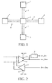
- FIG. 1 An embodiment of the network according to the invention is shown in FIG. 1.
- This network contains, for example, four network nodes 1 to 4, each of which is coupled to one another via an active star node 9 via twisted line pairs 5 to 8 (twisted pair) provided for symmetrical signal transmission.
- the active star node 9 carries out a line adaptation, so that the line pairs 5 to 8 in the active star node 9 are terminated with the characteristic impedance, and analyzes the signals transmitted by the network nodes 1 to 4. If the line pairs 5 to 8 were connected to each other without an active star node 9, a mismatch would result for each line pair in the star point due to the impedance jump from Z 0 to 1/3 Z 0 , which is caused by the parallel connection of the other line pairs.
- the active star node 9 contains a star interface for each line pair 5 to 8 forwarding a message from a sending network node to all others on active star connected network node.
- the basic circuit diagram of such Fig. 2 shows the star interface.
- a pair of lines 5 to 8 is switchable with the inputs Amplifier 10 (first switching element), which has a switching input 11, and with the outputs of a further switchable amplifier 12 (second switching element) coupled, which has a switching input 13.
- At the output of the switchable amplifier 10 there is a signal rec_data and a signal rec_en is present at its switching input 11.
- With the Output of amplifier 10 is coupled to an activity detector 14, which detects the output signal rec_data analyzed.
- the input of the switchable amplifier 12 receives an input signal drv_data Its switching input 13 receives the signal drv_en.
- the activity detector 14 can also be arranged in front of the amplifier 10 if it has its own Receiver amplifier and a switching input to switch off the activity detection having.
- the activity detector 14 of a star interface is used to identify certain ones Activities in a signal that the assigned star interface via the assigned line pair is supplied by the assigned network node and one indicates incoming transmission of a message. Such activity can for example a change in the signal level in a signal with certain subsequent signal changes mean. After detection of activity will be in the star node 9 then the other star interfaces switched so that they only one Receive message from the star interface that has a message from the associated one Node receives. This state of the star node is maintained until the assigned node has completely sent its message. This is done in the Star interface continuously checks whether the message is still being sent, i.e. if still activity at the output of the switchable amplifier 10 is detectable or whether the Sending has been completed (no activity).
- a message is to be issued by a network node, the network node must a certain activity is generated, which is referred to as a send request.
- a send request On Exemplary signal curve for a send request is shown in FIG. 3.
- the signal has three phases BI, CD and MD.
- the network node By changing the level at the end of phase BI and at the beginning of the CD phase, the network node indicates that it is transmitting a message want. This change in level is determined by the assigned star interface of the star node 9 detected and the switchable amplifier 12 of the associated star interface and the switchable amplifier 11 of the other star interfaces switched off and the switchable Amplifier 12 of the other star interfaces opened. If the other nodes do that received signal of the currently active transmission node, the phase begins MD (transfer of data).
- the time CD that a star interface in the star node 9 needed to recognize the signal edge, this against a fault distinguish and its and the amplifiers of the other star interfaces accordingly to switch must be considered by the sending network node before it Message.
- This time interval CD depends on the chosen one Implementation of the activity detection (selected activity detector 14) and the Number of star nodes in the network.
- the star node 9 in Fig. 1 can instead of one Network node with at least one further star node, to the others Network nodes are connected. In this case, the Send request from the star node 9 to the second star node are passed on and the configuration time of this second star node belongs to Phase CD. This is necessary so that the message to be sent also the Reach network nodes connected to the second star node.
- the star interface shown in Figure 2 is that on the link recognizes a level change to the connected network node, provided for this purpose Forward event to the other star interfaces of star node 9. That from The control signal act_det generated by the activity detector 14 is used to control the switchable Amplifiers 10 and 12 are used. The activity detector 14 activates the control signal act_det after detection of an activity. It remains active as long as there is a message Network goes through. The level changes within the message are considered an activity interpreted. If these changes fail to occur, the detector recognizes that the end of the Message is reached.
- An exemplary signal curve with the phases MD and BI at Fig. 4 shows an end of the message. The end of a message is indicated by a constant level (phase BI).
- the maximum time intervals constant Levels within the message must not be used to switch off the control signal lead act_det. Only after a time interval that a certain time does not Level change contains an end to the activity and thus the end of the message recognized.
- the control line act_det is then deactivated. This event will be sent to the other star interfaces and the connected amplifiers of these Star interfaces are switched off.
- the star node goes back to a state by responding to a new send request from any network node can and configure the data path in the network accordingly can.
- FIG. 5 shows an exemplary course of a signal of a network node with interference pulses and the control signal act_det generated therefrom by the activity detector 14.
- the delay T (act_det) is always greater than the tolerable interference pulse width, so that a distinction between the two events is possible at all. This is from that Activity detector 14 considered.
- the time period MD (max) gives the maximum time interval between two level changes within a message. This maximum time interval depends on the selected coding and the data rate.
- a transmission method for which the Time interval MD (max) cannot be determined, is for the use of activity detection not suitable for controlling active star networks. For example, at a Transmission method using the NRZ coding for an indefinite one No level changes occur for a period of time.
- the time interval T (BI) that the activity detector 14 needs is the end of one To reliably detect transmission, it must be larger than the maximum width MD (max) of one Impulse during a message. This is the only way to ensure that a connection does not abort during an ongoing message transmission
- the time interval T (BI) should be determined so that this is an additional safety time interval contains. This increases the likelihood of incorrect detection the end of a message transmission is reduced. This security time interval will due to various system inaccuracies (e.g. scanning errors in one digital edge detection, drift of component properties etc.).
- the principle of activity detection can generally be applied to any type of signal transmission apply, e.g. even on a single wire transmission, and is not on a symmetrical one Push-pull transmission limited.
- the decisive factor is the logical level, which corresponds to the Activity detector is supplied.
- FIG. 6 An exemplary embodiment of a star interface is shown in FIG. 6.
- One pair of lines is with the inputs of a switchable amplifier 15, with the outputs of another switchable amplifier 16, with an activity detector 17 and with a Terminating resistor 18 connected.
- the value of the terminating resistor 18 corresponds the wave resistance and thus serves for the correct line termination. If the Activity detector 17 detects a transmission request, this generates an activated one Control signal, which to a switching input 19 of the switchable amplifier 15, to a inverting input of an AND gate 20 and via an amplifier 21 to one Line 22 connected to a non-inverting input of AND gate 20 is. If the switchable amplifier 15 is released, this supplies data to one a data line 23 leading from a connection point.
- the amplifier 21 is realized in FIG. 6 as an "open drain” amplifier.
- the star interfaces of one Star nodes 9 are connected to their respective lines 22 and 23 in this case, so that two circuit nodes are formed.
- there is a resistance provide the one with the circuit node (line 22) and the other with the level logic "0" is coupled. This resistance forms together with the Amplify 21 of each star interface the wired-OR link.
- An 'open collector' Circuit for the amplifier 21 is with appropriate adaptation of the logic Linking through the AND gate 20 is also possible to the wired-OR link to realize.
- FIG. 7 The functional structure of an activity detector 14 or 17 can be seen in FIG. 7.
- This contains a filter 27 for suppressing interference, an edge detector 28 and an activity detection circuit 29.
- the on one of the wire pairs 5 to 8 incoming or lying at the output of a switchable amplifier becomes Interference suppression suppresses the filter 27.
- the filtered signal is from Edge detector 28 analyzed. This reports an edge or a flank, i.e. one Edge or level change of the activity detection circuit 29, which determines whether a Send request, a message or the end of a message is present.
- the functional structure from FIG. 7 can easily be applied to a digital exemplary embodiment, which is described below. In one also described 7, the functional blocks from FIG. 7 are not so clear assigned.
- FIG. 8 Fig. 8 An exemplary embodiment of a first digital activity detector is shown in FIG. 8 Fig. 8 shown switching elements require a common clock (clk).
- the frequency of this clock signal must be chosen so that sufficient oversampling the data signal is guaranteed. Is the shortest interval of constant level in the Given data flow through TB, the period of the clock signal in the star node may amount to a maximum of TB / 2.
- the digital circuit of FIG. 8 includes a filter 30, one Edge detector 31 and an activity detection circuit with one Send request memory 32 and an idle detection circuit 33 for detection the end of an activity.
- the filter 30 prevents an edge that is only caused by a short glitch the line pair was generated by the subsequent logic as a send request of the network node is interpreted.
- a filter can, for example, consist of a Shift registers (e.g. for 3 samples) with a subordinate evaluation logic exist.
- the subordinate evaluation logic is part of the edge detector 31 Samples pass through the shift register, whereby the oldest value is always dropped as soon as a new sample value is recorded.
- the edge detector 31 interprets the im Shift register stored values to determine whether a level change (signal edge) was actually caused by a sending network node.
- the filter 30 and the edge detector 31 can also be made more complex. By including more samples, the security with which an interference signal does not trigger the activity detection circuit. Indeed The filter 30 and the edge detector 31 must not have any number of samples for interpretation use, because this also delays the time between the occurrence of the Signal edge and the activation of the control signal is increased.
- the filter 30 also realizes analogously in order to eliminate interference, or the digital filter 30 is supplemented by an upstream, analog filter (low pass) can be.
- this information is stored in the send request memory 32.
- the feed in this memory e.g. via a synchronous set input.
- the output of the send request memory 32 is the control signal act_det, which - how explained above - to control your own but also the other star interfaces of the Star node 9 is used.
- the send request memory keeps the control signal act_det active until the Idle detection circuit 33 determines the end of the activity and then via one synchronous reset input 60 resets the send request memory 32.
- the control signal act_det is then deactivated.
- the Signal rec_data in Fig. 9 contains a disturbance N by the edge detector as such is recognized and does not cause a pulse in the output signal of the edge detector 31. Only when there is no pulse for a defined interval does the Idle detection circuit 33 its output signal. This output signal signals then that the end of the current message has been reached and sets the Send request memory 32 back.
- the idle detection circuit 33 may be a counter that after a release with an adjustable granularity (counting step size) begins to count towards its internal counter increment. By setting an overflow condition, a time interval can be set be defined, after which the counter activates its output signal.
- the counter can of course also be provided as a down counter with a the specified starting level begins and when the value falls below a lower limit (e.g. zero) appropriately activates its output signal.
- the output signal ED of the edge detector 31 is when the idle detection circuit is implemented 33 used as a counter, the counter reading to the initial state reset. As a result, the expiration condition of the counter is not reached, as long as the pulses in the output signal of the edge detector 31 in sufficiently short Follow intervals. These distances are determined by the type of coding Message and the data rate defined. Even the appearance of the longest, within one coded message possible time interval between two level changes must not cause the counter to reach its expiration counter.
- a dimensioning of this interval must therefore the type of message coding adjusted and the meter configured accordingly. This can be done, for example a programmable sequence or start counter can be realized. It is also possible to increase the counting step size using a configurable clock divider for the clock (clk) set so that the counter is fed an appropriately adapted counting cycle.
- the idle detection circuit 33 is enabled by the send request memory via connection 34.
- the first edge on a pair of lines 5 to 8 (send request) used to switch the Amplifier in the star interfaces for the subsequent message transmission adjust.
- the send request must therefore always have a specific time interval of the actual message, so that the amplifiers in the star node 9 can be switched and connecting paths in the star node Result in message transmission from one network node to the other network nodes, before the actual message transmission begins. It is therefore possible that between the first signal edge of the rec_data signal (see FIG. 9: first pulse in the output signal ED of the edge detector 31) and the first one caused by the message Signal edge (see FIG.
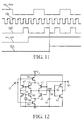
- FIG. 11 shows various signal profiles in the activity detector according to FIG. 10 From this results, the release signal EN for the idle detection circuit 33 is only with the first signal edge of the data message is activated. The idle detection circuit 33 therefore only checks from the beginning of the message whether the defined interval has no activity in the Signal rec_data is recognizable
- FIG. When using an analog activity detector, no clock source is required in the star node.
- the analog activity detector receives at its input 37 the signal rec_data, which is led to the gate connection of a P-channel MOS field-effect transistor 38 and to the gate connection of an N-channel MOS field-effect transistor 39.
- the source connection of transistor 39 is connected to ground and its drain connection is connected to the source connections of two N-channel MOS field-effect transistors 40 and 41.
- the source connection of transistor 38 is connected to a voltage supply V CC .
- the drain of transistor 38 is connected to the source connections of two P-channel MOS field-effect transistors 42 and 43, whose drain connections have a common node 58 with the drain connections of transistors 40 and 41, a connection of a capacitor 44 and the gate connection of an N-channel MOS field-effect transistor 45 and the gate connection of a P-channel MOS field-effect transistor 46.
- the gate of transistor 42 is connected to the gate and drain of a P-channel MOS field-effect transistor 47 and the drain of an N-channel MOS field-effect transistor 48.
- the source connection of the transistor 47 is connected to the voltage supply V CC .
- the gate connection of transistor 48 is connected on the one hand to the gate connection of transistor 40 and on the other hand to a voltage source 49 (V ref ).
- the other connection of the voltage source 49 is connected to ground, as is the source connection of the transistor 48.
- the gate connections of the transistors 41 and 43 and the drain connections of the transistors 45 and 46 form the output 50 of the analog activity detector which supplies the control signal act_det.
- the source connection of the transistor 46 is still connected to the voltage source V CC and the source connection of the transistor 45 as well as the other connection of the capacitor 44 to ground.
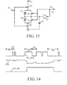
- adjustable resistor 51 is provided by voltage source 49 and transistors 42, 47 and 48 and an adjustable resistor 52 through the voltage source 49 and Transistor 40 formed.
- the transistor 38 provides a switch 53, the transistor 43 one Switch 54, transistor 41 a switch 55 and transistor 39 a switch 56
- the transistors 45 and 46 form an inverter 57.
- switches 53 and 54 are closed and switches 55 and 56 opened in the functional circuit diagram according to FIG. 13.
- the capacitor is over the Switches 53 and 54 charged.
- transistor 38 If there is a level change at input 37, i.e. the signal shows a high Voltage level, transistor 38 is switched off and transistor 39 open. A constant current then flows through the drain connection of the transistor 40, whereby the capacitor 44 discharges.
- short interference pulses occur. That means that For a short time there is a high voltage level (logical "1") in the rec_data signal. Such interference pulses are suppressed by a filter which is passed through the capacitor 44 and the resistance of transistor 40 is determined. If the interference pulses are very short, then the voltage at node 58 does not reach a switching threshold at which that from the Transistors 45 and 46 formed output stage tilts, i.e. output 50 (signal act_det) would pull to a high signal level. The signal at output 50 thus remains short interference pulses deactivated. After the short glitch ends, introduces low signal level at the input 37 means that the capacitor 44 over the switched on transistors 38 and 43 is recharged very quickly.
- the switches 53 and 55 are thus opened and in the function diagram 13 the switch 56 closed.
- a discharge current flows from the capacitor 44 through the Resistor 52 and switch 56 to ground.
- the capacitor 44 and the Resistor 52 determine the time constant of the discharge.
- the voltage level at input 37 is at least for a time interval of length T (act_det) at a high voltage level (see Fig. 5 taking into account the inverted Input level compared to Fig. 14).
- This causes the voltage at node 58 to drop the discharge via transistors 39 and 40 below the switching threshold of the output stage with transistors 45 and 46 (inverter).
- the output 50 changes to a high one Signal level, i.e. the control signal indicating a send request is activated.
- the Transistor 43 is thereby switched off and transistor 41 is switched on.
- the capacitor 44 is now suddenly complete discharged (see signal curve from ZW). The circuit thus achieves a stable one State that indicates activity.
- the third state Z3 can be done as follows explain. After a change in the signal level at input 37 to logic "1", the Switch 53 opened (55 remains open for the time being) and switch 56 closed. It flows a discharge current from capacitor 44 through resistor 52 and switch 56 after Mass from. After reaching the switching threshold determined by the inverter 57, the Switch 54 opened and switch 55 closed. This results in an increased Charge discharge via switches 55 and 56 to ground.
- Time intervals occur during which the actual message is being transmitted low voltage level is present at input 37. These time intervals are part of the Message and therefore these must not lead to a change in the signal level at output 50 to lead.
- a low input level at node 37 causes the Transistor 38 opens and transistor 39 is closed. This allows the No longer discharge capacitor through the path from transistors 39 and 41. about transistors 38 and 42 becomes capacitor 44 with a constant current which is dependent on the voltage source 49, charged (fourth state Z4).
- the Transistors 47 and 42 must be dimensioned so that the current flowing through 42 in the fourth state is smaller than that in the second or third state Discharge of the capacitor 44 has led through the transistor 40. This allows the Set the duration of the time interval for which a low voltage level at input 37 does not yet lead to a change in the signal level at output 50.
- the Activity detector thus remains activated as long as the time intervals are low Voltage level does not exceed a certain duration.
- the charging process of the capacitor 44 via the transistor 42 is therefore slower than one Discharge via transistor 40. Interference during data transmission just like low voltage levels, not affecting the control signal act_det at output 50. A subsequent high voltage level at input 50 provides for the capacitor 44 to be quickly discharged via transistors 41 and 39 and the detection circuit remains in its stable state.
- the fourth state Z4 can also be explained on the functional circuit diagram 13.
- the resistor 51 is selected such that after a change from a high to a low voltage level at the input 37 after opening the switch 56 and closing the switch 53, the capacitor 44 is slowly charged by the voltage source V CC .
- the resulting resistances of transistor 40 and Transistor 42 are dimensioned accordingly.
- the resistance of transistor 40 corresponds to resistor 52 in FIG. 13), which determines the response time of the detector, is smaller than the resistance of transistor 42 (resistor 51 in FIG. 13), which for the Time interval, which is regarded as the end of the activity, is decisive.
- the voltage source 49 shown in FIG. 12 can be obtained from a reference current source in Connection can be realized with a known transistor diode connection.
- the difference between the time intervals in the message with constant level and the switch-off condition (an interval without activity, which is a defined length) must be determined by the dimensioning of the different Transistors - as mentioned above - are guaranteed. However, the time intervals are depending on the data rate at which a transmission is carried out.
- the Voltage source 49 can be carried out programmably. With the adjustable Charging current, the charging time constant of the capacitor 44 is configurable. A Programming the activity detection circuit to a desired data rate can e.g. by additional control lines for setting the reference voltage on the Voltage source 49 can be realized.
- the transistor 47 can also be replaced by a voltage source.
- the Capacitor 44 need not be present as an independent element, but can also be are formed by the parasitic capacitances, which the input capacitances of the Form transistors 45 and 46.
- FIG. 15 shows another embodiment for the analog activity detection Compared to FIG. 12, the circuit contains a further P-channel field effect transistor 59, its source connection alone with the drain connection of transistor 43, its gate connection with the gate of transistor 42 and its drain the drain of transistor 41, the gates of transistors 45 and 46 and is connected to a connection of the capacitor 44.
- Opposite Fig 12 points 15 shows no connection on the one hand between the drain connections of the transistors 40 and 42 and the gate connections of transistors 45 and 46.
- the transistor 59 increases the time constant for the charging of the capacitor 44, i.e. it takes time longer to raise the potential at node 58. This increases immunity Circuit against interference pulses on the line.
Landscapes
- Engineering & Computer Science (AREA)
- Computer Networks & Wireless Communication (AREA)
- Signal Processing (AREA)
- Small-Scale Networks (AREA)
Applications Claiming Priority (2)
| Application Number | Priority Date | Filing Date | Title |
|---|---|---|---|
| DE10039838A DE10039838A1 (de) | 2000-08-10 | 2000-08-10 | Aktivitätsdetektion in einem Sternknoten mit mehreren gekoppelten Netzknoten |
| DE10039838 | 2000-08-10 |
Publications (3)
| Publication Number | Publication Date |
|---|---|
| EP1179921A2 true EP1179921A2 (fr) | 2002-02-13 |
| EP1179921A3 EP1179921A3 (fr) | 2004-05-19 |
| EP1179921B1 EP1179921B1 (fr) | 2006-10-18 |
Family
ID=7652495
Family Applications (1)
| Application Number | Title | Priority Date | Filing Date |
|---|---|---|---|
| EP01000360A Expired - Lifetime EP1179921B1 (fr) | 2000-08-10 | 2001-08-09 | Détection d'activité dans un noeud central couplé à plusieurs noeuds |
Country Status (7)
| Country | Link |
|---|---|
| US (1) | US7035224B2 (fr) |
| EP (1) | EP1179921B1 (fr) |
| JP (1) | JP2002101117A (fr) |
| KR (1) | KR100793451B1 (fr) |
| CN (1) | CN1227871C (fr) |
| DE (2) | DE10039838A1 (fr) |
| ES (1) | ES2273749T3 (fr) |
Families Citing this family (8)
| Publication number | Priority date | Publication date | Assignee | Title |
|---|---|---|---|---|
| US7304994B2 (en) * | 2003-04-09 | 2007-12-04 | Nec Laboratories America, Inc. | Peer-to-peer system and method with prefix-based distributed hash table |
| KR100703688B1 (ko) * | 2004-10-18 | 2007-04-05 | 삼성전자주식회사 | 다수의 네트워크 정보를 선택적으로 표시하는 방법 및네트워크 장치 |
| DE102007050708B4 (de) * | 2007-10-22 | 2009-08-06 | Phoenix Contact Gmbh & Co. Kg | System zum Betreiben wenigstens eines nicht-sicherheitskritischen und wenigstens eines sicherheitskritischen Prozesses |
| US20160277208A1 (en) | 2015-03-18 | 2016-09-22 | GM Global Technology Operations LLC | Vehicle communication system |
| CN109141389B (zh) * | 2018-09-20 | 2021-03-26 | 桂林电子科技大学 | 一种电罗经信号模拟发生器 |
| CN115210398B (zh) | 2020-02-28 | 2023-09-26 | 杰富意钢铁株式会社 | 钢板、构件和它们的制造方法 |
| WO2021172298A1 (fr) | 2020-02-28 | 2021-09-02 | Jfeスチール株式会社 | Tôle d'acier, élément et procédés respectivement pour la production de ladite tôle d'acier et dudit élément |
| JP7006848B1 (ja) | 2020-02-28 | 2022-01-24 | Jfeスチール株式会社 | 鋼板、部材及びそれらの製造方法 |
Family Cites Families (18)
| Publication number | Priority date | Publication date | Assignee | Title |
|---|---|---|---|---|
| US4428046A (en) | 1980-05-05 | 1984-01-24 | Ncr Corporation | Data processing system having a star coupler with contention circuitry |
| US4663748A (en) * | 1984-04-12 | 1987-05-05 | Unisearch Limited | Local area network |
| US4781427A (en) * | 1985-09-19 | 1988-11-01 | The Mitre Corporation | Active star centered fiber optic local area network |
| US4700344A (en) * | 1986-06-13 | 1987-10-13 | Ncr Corporation | Processor overrun circuit |
| US5434861A (en) * | 1989-02-02 | 1995-07-18 | Pritty; David | Deterministic timed bus access method |
| US5073982A (en) * | 1989-09-01 | 1991-12-17 | General Electric Company | Apparatus for connecting multiple passive stars in a fiber optic network |
| GB8923351D0 (en) * | 1989-10-17 | 1989-12-06 | Stc Plc | Multifrequency optical network |
| US5127067A (en) * | 1990-09-10 | 1992-06-30 | Westinghouse Electric Corp. | Local area network with star topology and ring protocol |
| ES2145846T3 (es) * | 1993-11-08 | 2000-07-16 | British Telecomm | Sistema de interconexion para una red optica. |
| JPH0897782A (ja) * | 1994-09-22 | 1996-04-12 | Matsushita Electric Ind Co Ltd | 通信回線割付け装置の回線監視方法 |
| US6000003A (en) * | 1994-09-29 | 1999-12-07 | Maxim Integrated Products, Inc. | Communication circuit having network connection detection capability |
| WO1996033590A1 (fr) * | 1995-04-21 | 1996-10-24 | Illinois Institute Of Technology | Procede et appareil pour la transmission de donnees numeriques de file d'attente reparties au moyen de tranches de donnees de longueur variable |
| US5859837A (en) * | 1995-06-07 | 1999-01-12 | Advanced Micro Devices Inc. | Flow control method and apparatus for ethernet packet switched hub |
| US6115032A (en) * | 1997-08-11 | 2000-09-05 | Cirrus Logic, Inc. | CRT to FPD conversion/protection apparatus and method |
| JP3566846B2 (ja) * | 1997-12-24 | 2004-09-15 | 古河電気工業株式会社 | 多重通信方法 |
| US6198722B1 (en) * | 1998-02-27 | 2001-03-06 | National Semiconductor Corp. | Flow control method for networks |
| ES2274763T3 (es) * | 1999-09-16 | 2007-06-01 | Koninklijke Philips Electronics N.V. | Red con varios nudos de red y al menos un nudo en estrella. |
| DE10016829A1 (de) * | 2000-04-06 | 2001-10-11 | Philips Corp Intellectual Pty | Auflösung von Medienzugriffskonflikten in Netzwerken mit mehreren Netzknoten und wenigstens einem Sternknoten |
-
2000
- 2000-08-10 DE DE10039838A patent/DE10039838A1/de not_active Withdrawn
-
2001
- 2001-08-06 CN CNB011328606A patent/CN1227871C/zh not_active Expired - Fee Related
- 2001-08-07 US US09/923,609 patent/US7035224B2/en not_active Expired - Lifetime
- 2001-08-09 EP EP01000360A patent/EP1179921B1/fr not_active Expired - Lifetime
- 2001-08-09 KR KR1020010047862A patent/KR100793451B1/ko not_active Expired - Fee Related
- 2001-08-09 ES ES01000360T patent/ES2273749T3/es not_active Expired - Lifetime
- 2001-08-09 DE DE50111253T patent/DE50111253D1/de not_active Expired - Lifetime
- 2001-08-10 JP JP2001243629A patent/JP2002101117A/ja not_active Withdrawn
Also Published As
| Publication number | Publication date |
|---|---|
| EP1179921B1 (fr) | 2006-10-18 |
| JP2002101117A (ja) | 2002-04-05 |
| KR20020013733A (ko) | 2002-02-21 |
| DE10039838A1 (de) | 2002-02-21 |
| US7035224B2 (en) | 2006-04-25 |
| DE50111253D1 (de) | 2006-11-30 |
| EP1179921A3 (fr) | 2004-05-19 |
| US20020048274A1 (en) | 2002-04-25 |
| KR100793451B1 (ko) | 2008-01-14 |
| ES2273749T3 (es) | 2007-05-16 |
| CN1227871C (zh) | 2005-11-16 |
| CN1338848A (zh) | 2002-03-06 |
Similar Documents
| Publication | Publication Date | Title |
|---|---|---|
| DE4429953B4 (de) | Serielles Bussystem | |
| EP2700017B1 (fr) | Procédé et dispositif pour la transmission de données en série avec codage de données à commutation | |
| DE60128703T2 (de) | Zweirichtungszwischenverstärker mit hoch/niedrig-schwellendetektionsschaltung | |
| EP0725513A1 (fr) | Etage final, tolérant des fautes, pour un système digital de communication de données de configuration bus bifilaire | |
| DE19750317B4 (de) | Empfangsschaltung für ein CAN-System | |
| DE4307794C2 (de) | Einrichtung zur Überwachung symmetrischer Zweidraht-Busleitungen und -Busschnittstellen | |
| EP1179921A2 (fr) | Détection d'activité dans un noeud central couplé à plusieurs noeuds | |
| DE4211579C1 (de) | Verfahren zur Überwachung symmetrischer Zweidraht-Busleitungen und -Busschnittstellen, und Vorrichtung zur Durchführung des Verfahrens | |
| DE10146585A1 (de) | Verfahren und Schaltungsanordnung zur Anpassung des Spannungspegels für die Übertragung von Daten | |
| EP2487660B1 (fr) | Installation d'alerte aux dangers | |
| DE19960785A1 (de) | Eingangsfilterstufe für einen Datenstrom und Verfahren zum Filtern eines Datenstroms | |
| DE102010046964A1 (de) | Ladungspumpe | |
| DE3826509C2 (fr) | ||
| EP1787206B1 (fr) | Dispositif de transmission de signal | |
| DE102009050692B4 (de) | Sicherheits-Kommunikationssystem zur Signalisierung von Systemzuständen | |
| EP0332055B1 (fr) | Circuit pour la détection de niveaux défectueux de signaux numériques qui sont injectés sur un bus | |
| AT402587B (de) | Schaltungsanordnung zum übertragen von binären signalen zwischen mehreren teilnehmern | |
| EP0727897B1 (fr) | Circuit de réception d'un signal transmis sur un bus comme variations d'un niveau de tension | |
| EP4054128B1 (fr) | Procédé d'initialisation d'un système de bus de communication série | |
| DE102021122843A1 (de) | Übertragungssystem und Übertragungsverfahren zur Übertragung von Daten und Energie über eine Zweidrahtleitung | |
| EP1193890B1 (fr) | Méthode et appareil pour diagnostiquer une ligne de transmission d'un système de bus | |
| WO2023031017A1 (fr) | Système de transmission et procédé de transmission pour transmettre des données et de l'énergie par l'intermédiaire d'une ligne à deux fils | |
| DE3010535C2 (de) | Regenerator für digitale Signale | |
| EP1143668B1 (fr) | Solution des conflits d'acces aux supports dans des réseaux avec plusieurs noeuds et au moins un noed central | |
| DE602004011332T2 (de) | Kommunikationsnetz und verfahren zur steurung des kommunikationsnetzes |
Legal Events
| Date | Code | Title | Description |
|---|---|---|---|
| PUAI | Public reference made under article 153(3) epc to a published international application that has entered the european phase |
Free format text: ORIGINAL CODE: 0009012 |
|
| AK | Designated contracting states |
Kind code of ref document: A2 Designated state(s): AT BE CH CY DE DK ES FI FR GB GR IE IT LI LU MC NL PT SE TR |
|
| AX | Request for extension of the european patent |
Free format text: AL;LT;LV;MK;RO;SI |
|
| RAP1 | Party data changed (applicant data changed or rights of an application transferred) |
Owner name: PHILIPS CORPORATE INTELLECTUAL PROPERTY GMBH Owner name: KONINKLIJKE PHILIPS ELECTRONICS N.V. |
|
| RAP1 | Party data changed (applicant data changed or rights of an application transferred) |
Owner name: KONINKLIJKE PHILIPS ELECTRONICS N.V. Owner name: PHILIPS INTELLECTUAL PROPERTY & STANDARDS GMBH |
|
| PUAL | Search report despatched |
Free format text: ORIGINAL CODE: 0009013 |
|
| AK | Designated contracting states |
Kind code of ref document: A3 Designated state(s): AT BE CH CY DE DK ES FI FR GB GR IE IT LI LU MC NL PT SE TR |
|
| AX | Request for extension of the european patent |
Extension state: AL LT LV MK RO SI |
|
| RIC1 | Information provided on ipc code assigned before grant |
Ipc: 7H 04L 12/40 B Ipc: 7H 04L 12/44 A |
|
| 17P | Request for examination filed |
Effective date: 20041119 |
|
| 17Q | First examination report despatched |
Effective date: 20041223 |
|
| AKX | Designation fees paid |
Designated state(s): DE ES FR GB IT |
|
| GRAP | Despatch of communication of intention to grant a patent |
Free format text: ORIGINAL CODE: EPIDOSNIGR1 |
|
| RIN1 | Information on inventor provided before grant (corrected) |
Inventor name: HEUTS, PATRICK,PHILIPS CORP. INTEL. PROP. GMBH Inventor name: BUDDE,WOLFGANG, DR. O.PHILIPS CORP. IN. PROP.GMBH Inventor name: BOEZEN, HENKPHILIPS CORP. INTEL. PROP. GMBH Inventor name: FUHRMANN, PETER,PHILIPS CORP. INTEL. PROP. GMBH |
|
| GRAS | Grant fee paid |
Free format text: ORIGINAL CODE: EPIDOSNIGR3 |
|
| GRAA | (expected) grant |
Free format text: ORIGINAL CODE: 0009210 |
|
| AK | Designated contracting states |
Kind code of ref document: B1 Designated state(s): DE ES FR GB IT |
|
| PG25 | Lapsed in a contracting state [announced via postgrant information from national office to epo] |
Ref country code: IT Free format text: LAPSE BECAUSE OF FAILURE TO SUBMIT A TRANSLATION OF THE DESCRIPTION OR TO PAY THE FEE WITHIN THE PRESCRIBED TIME-LIMIT;WARNING: LAPSES OF ITALIAN PATENTS WITH EFFECTIVE DATE BEFORE 2007 MAY HAVE OCCURRED AT ANY TIME BEFORE 2007. THE CORRECT EFFECTIVE DATE MAY BE DIFFERENT FROM THE ONE RECORDED. Effective date: 20061018 |
|
| REG | Reference to a national code |
Ref country code: GB Ref legal event code: FG4D Free format text: NOT ENGLISH |
|
| REF | Corresponds to: |
Ref document number: 50111253 Country of ref document: DE Date of ref document: 20061130 Kind code of ref document: P |
|
| GBT | Gb: translation of ep patent filed (gb section 77(6)(a)/1977) |
Effective date: 20061129 |
|
| REG | Reference to a national code |
Ref country code: GB Ref legal event code: 732E |
|
| REG | Reference to a national code |
Ref country code: FR Ref legal event code: TP |
|
| REG | Reference to a national code |
Ref country code: ES Ref legal event code: FG2A Ref document number: 2273749 Country of ref document: ES Kind code of ref document: T3 |
|
| ET | Fr: translation filed | ||
| PLBE | No opposition filed within time limit |
Free format text: ORIGINAL CODE: 0009261 |
|
| STAA | Information on the status of an ep patent application or granted ep patent |
Free format text: STATUS: NO OPPOSITION FILED WITHIN TIME LIMIT |
|
| 26N | No opposition filed |
Effective date: 20070719 |
|
| PGFP | Annual fee paid to national office [announced via postgrant information from national office to epo] |
Ref country code: IT Payment date: 20120711 Year of fee payment: 12 Ref country code: ES Payment date: 20120717 Year of fee payment: 12 |
|
| REG | Reference to a national code |
Ref country code: DE Ref legal event code: R082 Ref document number: 50111253 Country of ref document: DE Representative=s name: PATENTANWAELTE RUFF, WILHELM, BEIER, DAUSTER &, DE |
|
| REG | Reference to a national code |
Ref country code: DE Ref legal event code: R081 Ref document number: 50111253 Country of ref document: DE Owner name: PARTNERS FOR CORPORATE RESEARCH CV, KY Free format text: FORMER OWNER: NXP B.V., EINDHOVEN, NL Effective date: 20130322 Ref country code: DE Ref legal event code: R082 Ref document number: 50111253 Country of ref document: DE Representative=s name: PATENTANWAELTE RUFF, WILHELM, BEIER, DAUSTER &, DE Effective date: 20130322 Ref country code: DE Ref legal event code: R081 Ref document number: 50111253 Country of ref document: DE Owner name: PARTNERS FOR CORPORATE RESEARCH CV, GEORGE TOW, KY Free format text: FORMER OWNER: NXP B.V., EINDHOVEN, NL Effective date: 20130322 |
|
| PG25 | Lapsed in a contracting state [announced via postgrant information from national office to epo] |
Ref country code: IT Free format text: LAPSE BECAUSE OF NON-PAYMENT OF DUE FEES Effective date: 20130809 |
|
| REG | Reference to a national code |
Ref country code: ES Ref legal event code: FD2A Effective date: 20140908 |
|
| PG25 | Lapsed in a contracting state [announced via postgrant information from national office to epo] |
Ref country code: ES Free format text: LAPSE BECAUSE OF NON-PAYMENT OF DUE FEES Effective date: 20130810 |
|
| PGFP | Annual fee paid to national office [announced via postgrant information from national office to epo] |
Ref country code: GB Payment date: 20140806 Year of fee payment: 14 Ref country code: FR Payment date: 20140808 Year of fee payment: 14 |
|
| GBPC | Gb: european patent ceased through non-payment of renewal fee |
Effective date: 20150809 |
|
| REG | Reference to a national code |
Ref country code: FR Ref legal event code: ST Effective date: 20160429 |
|
| PG25 | Lapsed in a contracting state [announced via postgrant information from national office to epo] |
Ref country code: GB Free format text: LAPSE BECAUSE OF NON-PAYMENT OF DUE FEES Effective date: 20150809 |
|
| PG25 | Lapsed in a contracting state [announced via postgrant information from national office to epo] |
Ref country code: FR Free format text: LAPSE BECAUSE OF NON-PAYMENT OF DUE FEES Effective date: 20150831 |
|
| PGFP | Annual fee paid to national office [announced via postgrant information from national office to epo] |
Ref country code: DE Payment date: 20170822 Year of fee payment: 17 |
|
| REG | Reference to a national code |
Ref country code: DE Ref legal event code: R119 Ref document number: 50111253 Country of ref document: DE |
|
| PG25 | Lapsed in a contracting state [announced via postgrant information from national office to epo] |
Ref country code: DE Free format text: LAPSE BECAUSE OF NON-PAYMENT OF DUE FEES Effective date: 20190301 |