EP1179933A2 - Liaison sans fil pour données numériques - Google Patents
Liaison sans fil pour données numériques Download PDFInfo
- Publication number
- EP1179933A2 EP1179933A2 EP01119378A EP01119378A EP1179933A2 EP 1179933 A2 EP1179933 A2 EP 1179933A2 EP 01119378 A EP01119378 A EP 01119378A EP 01119378 A EP01119378 A EP 01119378A EP 1179933 A2 EP1179933 A2 EP 1179933A2
- Authority
- EP
- European Patent Office
- Prior art keywords
- digital data
- data transmission
- circuit
- transmitter
- transmission link
- Prior art date
- Legal status (The legal status is an assumption and is not a legal conclusion. Google has not performed a legal analysis and makes no representation as to the accuracy of the status listed.)
- Withdrawn
Links
- 230000005540 biological transmission Effects 0.000 claims abstract description 74
- 230000006978 adaptation Effects 0.000 claims description 22
- 238000011144 upstream manufacturing Methods 0.000 claims description 7
- 230000000295 complement effect Effects 0.000 claims description 2
- 239000003365 glass fiber Substances 0.000 claims 1
- 238000006243 chemical reaction Methods 0.000 description 2
- 238000011161 development Methods 0.000 description 2
- 230000018109 developmental process Effects 0.000 description 2
- 238000005070 sampling Methods 0.000 description 2
- 239000013078 crystal Substances 0.000 description 1
- 230000009977 dual effect Effects 0.000 description 1
- 239000013307 optical fiber Substances 0.000 description 1
- 239000010453 quartz Substances 0.000 description 1
- 238000007493 shaping process Methods 0.000 description 1
- 230000008054 signal transmission Effects 0.000 description 1
- VYPSYNLAJGMNEJ-UHFFFAOYSA-N silicon dioxide Inorganic materials O=[Si]=O VYPSYNLAJGMNEJ-UHFFFAOYSA-N 0.000 description 1
- 230000005236 sound signal Effects 0.000 description 1
Images

Classifications
-
- H—ELECTRICITY
- H04—ELECTRIC COMMUNICATION TECHNIQUE
- H04L—TRANSMISSION OF DIGITAL INFORMATION, e.g. TELEGRAPHIC COMMUNICATION
- H04L25/00—Baseband systems
Definitions
- the present invention relates to a digital data transmission link, in particular for Transmission of digital audio data, with one transmitter, with one to be broadcast digital data stream is applied, and with a receiver that sends the digital data stream is applied.
- Such a digital data transmission link has been used, for example, to Stereo signals from a source device, such as a CD player, cordlessly to one Transfer headphones.
- a disadvantage of previous data transmission links of this type is that they are not 1: 1 data transmission, i.e. do not allow lossy data transmission.
- data reduction algorithms are used here in order to Ensure the available transmission range in the megahertz range. For high quality data transmission between e.g. a CD player and active The known transmission lines were therefore not used for loudspeakers.
- multicore arrangements in which, for example, analog from a stage via microphones Signals to a remote station, such as a recording and sending car be transmitted.
- a remote station such as a recording and sending car be transmitted.
- This way of transmitting analog signals is due to the relatively long and with cables to be overcome distances with losses and, among other things, also because of Laying of multicore cables required on site, costly.
- An object of the present invention is to overcome the above Disadvantages mentioned to create a digital data transmission link that cost-effective design a lossless transmission of a digital data stream guaranteed.
- Another object of the present invention is existing multicore arrangements inexpensive to replace lossless signal transmission.
- the core of the invention is a signal matching circuit that the to be sent digital data stream undergoes a waveform conversion such that the converted digital Data stream without problems, i.e. can be sent lossless by the transmitter.
- This Data stream can be easily received by the receiver and then by the Receiver arrangement are processed.
- the original digital data stream is recovered on the receiver side in that in the Receiving arrangement a signal matching circuit complementary to the transmitter arrangement is provided, which recovers the original waveform of this data stream 1: 1.
- the signal matching circuit (s) according to the invention can be used with conventional ones Components can be realized extremely inexpensively, so that the digital Data transmission path can be provided inexpensively overall, as this in rest on a conventional inexpensive transmitter and a conventional inexpensive receiver can be based.
- the transmission frequency required for lossless digital data transmission can, as such known to be located in the megahertz range.
- the transmission frequency is arranged in the gigahertz range.
- the gigahertz range also has the advantage that a much larger usable Bandwidth is available, so that an even larger data stream than in Megahertz range can be transmitted.
- the invention is based on the knowledge that so far a lossless one Data transfer with cost-effective implementation was not possible because the Signal form of the digital data stream to be sent from the transmitter (and from the receiver) not could be processed without loss. Because the amplitude of the digital data stream is not was optimally adapted to the transmitter (and receiver) and because in particular the shape, i.e. especially the edge of the signal of the digital data stream does not match the circumstances of the Transmitter was adjusted. This disadvantage is caused by the invention Signal matching circuit in the transmitter arrangement overcome.
- the invention is suitable Transmission path for high quality wireless transmission of audio signals e.g. to active speakers.
- a preferred embodiment of the digital transmission path is in the claims 15 to 31 both in terms of transmitter arrangement and receiver arrangement, and Although based on conventional components that are integrated and therefore miniaturized space-saving form are available inexpensively.
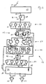
- the embodiment of a wireless digital shown in Figs. 1 and 2 Data transmission path is a two-channel transmission path, for example to Transfer of digital audio data designed.
- this digital link is not limited to two channels, but can easily with currently available means for example, expanded to 384 channels.
- the data can also "format-free", not organized in channels, are transmitted.
- the arrangement of the digital data transmission link shown on the transmitter side comprises an analog / digital converter on the input side (hereinafter referred to as A / D converter designated) 10 and on the output side a transmitter 11 for transmitting digital data.
- a / D converter designated On the sending digital data stream, which is output by the A / D converter 10, with full Information content about the transmitter 11 about the receiver arrangement shown in FIG. 2
- To be able to transmit is between the D / A converter 10 and the transmitter 11
- Signal adaptation stage 12 arranged, the output from the D / A converter 10 Data stream processed before feeding into the transmitter 11 so that a lossless Data transmission is guaranteed by the transmitter 11 to the receiver.
- the D / A converter 10 which is preferably a converter with a resolution of is at least 24 bits and a sampling rate of at least 96 kilohertz is in the illustrated embodiment used as a two-channel A / D converter.
- the A / D converter 10 comprises two inputs 13 and 14 for feeding analog (stereo) signals into the A / D converter 10.
- a digital data stream is present at the output 15 of the A / D converter 10, the one digital image of the analog signals originally fed into inputs 13, 14 represents and is for example in S / PDIF format.
- At two further exits 16, 17 of the A / D converter 10 are clock signals of the converter.
- WCLK Word Clock
- LRCK Left Right Clock
- the S / PDIF signal or data stream is at the output 15 by a trapezoidal waveform and an amplitude of Characteristically marked 0.5 volts.
- the transmitter 11 and the corresponding receiver
- this signal form is not lossless processed and emitted via the transmitter 11 and received losslessly by the receiver can be.
- the signal matching circuit 12 switched, which is explained in more detail below is.
- the signal matching circuit 12 comprises as an input stage one of the S / PDIF signal on Output 15 of the A / D converter 10 loaded buffer circuit 18, consisting of five Inverter stages 19 to 23 connected in parallel, to which a further inverter stage 24 is connected in series is connected upstream, the input side with the output 15 of the A / D converter 10 and is grounded on the output side via a quartz crystal 25.
- the buffer circuit 18 preferably consists of the six inverter stages one integrated hex. inverter.
- the output stage 18 is followed by an amplitude adjustment circuit in the adjustment circuit 12 26 in the form of a flip-flop circuit or a dual flip-flop.
- the digital data stream at the output of the buffer circuit 18 is in the D input of a first Flip-flop 27 and the D input of a second flip-flop 28 are fed.
- the clock inputs of the two flip-flops 27 and 28 are connected to the clock output 17 of the A / D converter 10, which carries the LRCK clock.
- The is at the Q outputs of the two flip-flops 27, 28
- Output of the circuitry 18 applied digital data stream with an amplitude on TTL or HC level is raised, namely to an amplitude of 3 volts.
- This Data stream is fed into a NAND gate circuit 29.
- the NAND gate circuit 29 includes four NAND gates 30, 31, 32 and 33.
- the two Inputs of the NAND gate 30 are common to the output 17 of the A / D converter 10 connected and thereby acted on with the LRCK clock. Besides, the two are Inputs of the NAND gate 30 connected via a resistor 34.
- the exit of the NAND gate 30 is connected to one input of NAND gate 31, the other of which Input is connected to the Q output of flip-flop 28.
- the output of the NAND gate 31 is connected to one input of NAND gate 33, the other input of which is connected to the output of the NAND gate 33.
- An input of the NAND gate 32 is connected to the Q output of flip-flop 27 and the other input of the NAND gate 32 is connected to the output 17 of the A / D converter 10, which is the LRCK clock signal leads.
- the output of the NAND gate 33 forms the output of the NAND gate circuit 29.
- a digital data stream is present at this output, the edges of which are in with respect to the original data stream at output 15 of the A / D converter is steeper run.
- the data stream has at the output of the NAND gate circuit 29 Rectangular shape, while the waveform of the output signal of the A / D converter like cited above, has a trapezoidal shape.
- An inverter circuit 34 for serial connection is connected to the NAND gate circuit 29 Output of the digital data stream from the NAND gate circuit 29 on.
- the Inverter circuit 34 is connected through a resistor 35 to the output of the NAND gate circuit 29 connected.
- the inverter circuit 34 comprises four EXOR gates 36, 37, 38 and 39.
- An input of EXOR gate 36 is connected to the output of NAND gate circuit 29 connected through resistor 35, and the other input of the EXOR gate 36 is connected to the clock output 16 of the A / D converter 10, which WLCK clock signal leads.
- the output of the EXOR gate 36 is connected to the output of the EXOR gate 38 and the output of EXOR gate 39 connected to these outputs jointly determine the output of the inverter circuit 34.
- the two inputs of the EXOR gates 37 are on positive supply voltage (5DVDD) for the Inverter circuit 34 and the output of the EXOR gate 37 is connected to both inputs of the EXOR gate 38 connected.
- the two inputs of EXOR gate 39 are grounded (DGND).
- Buffer circuit 40 is similar to buffer circuit 18 with five buffer stages connected in parallel 41 to 45.
- This buffer circuit 40 is on the input side with the output of Inverter circuit 34 and on the output side with an amplitude clipping circuit 46 connected, which is connected on the output side to the input 47 of the transmitter 11.
- the Amplitude clipping circuit 46 comprises a buffer stage 48, its input and output is bridged by a resistor 49. With buffer levels 41 to 45 and 48 it can are the six buffer levels of a hex inverter.
- the upstream adaptation circuit 12 accordingly emits the transmitter 11 with a digital data stream, whose waveform is derived from the original Data signal stream of the D / A converter 10 in terms of amplitude and slope is designed so that this data stream is transmitted without any problems by the transmitter 11, i.e. without loss can be.
- the receiver arrangement of the invention is in the following digital data transmission route explained.
- the receiver arrangement comprises a receiver 50 with an antenna 51 which is connected wirelessly an antenna 11a of the transmitter 11 communicates.
- the antennas 11a and 51 can alternatively be replaced by an optical fiber transmission link.
- the receiver arrangement comprising the receiver 50 on the input side comprises on the output side a digital / analog converter (hereinafter referred to as D / A converter) 52, preferably with a resolution of at least 24 bits and a sampling rate of at least 96 kHz, which are followed by buffer / low-pass filter circuits 53 and 54 on the output side the outputs of which are connected to the recovered analog signals which are input 13 and 14 of the A / D converter 10 have been input in the transmitter arrangement of FIG. 1.
- a signal matching circuit 55 is located between the receiver 50 and the D / A converter 52 switched, the compliment of the signal shaping sections Signal matching circuit 12 in the transmitter arrangement shown in FIG. 1 and the rest Upstream and downstream buffer circuits similar to the arrangement of FIG. 1 having.
- the output 55 of the receiver 50 is followed by an amplitude clipping circuit 56 in Shape of a buffer stage 27, its input and output with a resistor 58 is bridged.
- Amplitude clipping circuit 56 is followed by one Buffer circuit 59 on, which comprises five buffer stages 60 to 64 connected in parallel.
- the buffer circuit 59 is followed by a flip-flop circuit 65 for recovering the Original signal amplitude of the digital data stream at output 15 of the A / D converter in the amount of about 0.5 volts.
- This flip-flop circuit comprises two flip-flops 66 and 67. The D input of flip-flop 66 and the D input of flip-flop 67 are connected to the output of the Flip-flop circuit connected. The clock input of the flip-flop 66 and the clock input of the Flip-flops 67 are connected to a clock output 68 of the D / A converter 52, which is a LRCK signal leads.
- the Q output of flip-flop 66 and the Q output of flip-flop 67 are connected downstream of the amplitude adjustment circuit 65
- Signal edge matching circuit connected in the form of a NAND gate circuit 69, the comprises four NAND gates 70, 71, 72 and 73.
- An input of the NAND gate 70 is connected to the Q output of the flip-flop 67.
- the other input of NAND gate 70 is connected to the Q output of flip-flop 67.
- the other input of NAND gate 70 is at the output of NAND gate 71 connected.
- the two inputs of the NAND gate 71 are connected to ground (DGND).
- the output of the NAND gate 70 is connected to an input of the NAND gate 73.
- the other input of NAND gate 73 is at the output of NAND gate 72 connected, one input of which is connected to the Q output of flip-flop 66 and whose other output is connected to the clock output 68 of the D / A converter, which the LRCK signal leads.
- the output of the NAND gate 73 forms the output of the NAND gate stage 69th
- the NAND gate stage 69 which is the original slope of the digital Data stream at the output 15 of the A / D converter 10 is recovered with a Inverter circuit 74 connected, which includes four EXOR gates 75, 76, 77 and 78 and so serves, the data of the digital data stream from the NAND gate circuit 69 serially issue.
- An input of the EXOR gate 75 is with its output and an input of EXOR gate 76 connected, while the other input of EXOR gate 75 to the Output of the NAND gate circuit 69 (output of the NAND gate 73) is connected.
- EXOR gate 76 is with a clock output carrying a WRCK signal 89 of D / A converter 52 connected, while the output of EXOR gate 76 with both inputs of EXOR gate 77 and the output of EXOR gate 78 connected is.
- the two inputs of EXOR gate 78 are positive Supply voltage of the inverter circuit 74 is applied.
- the output of EXOR gate 77 forms the output of the inverter circuit 74.
- inverter circuit 74 is with an amplitude clipping circuit 79 connected, which comprises a buffer stage 80, the input and output of which by means of a resistor 81 is bridged and forms part of an integrated hex.
- Inverter the rest five buffer stages 82 to 86 form the parallel stages of a buffer circuit 87, between the amplitude clipping circuit 79 and the data stream input 88 of the D / A converter 52 is switched.
- the recovered digital is thus at input 88
Landscapes
- Engineering & Computer Science (AREA)
- Computer Networks & Wireless Communication (AREA)
- Signal Processing (AREA)
- Dc Digital Transmission (AREA)
- Optical Communication System (AREA)
- Cable Transmission Systems, Equalization Of Radio And Reduction Of Echo (AREA)
- Mobile Radio Communication Systems (AREA)
Applications Claiming Priority (2)
| Application Number | Priority Date | Filing Date | Title |
|---|---|---|---|
| DE10039187 | 2000-08-10 | ||
| DE10039187A DE10039187A1 (de) | 2000-08-10 | 2000-08-10 | Drahtfreie digitale Datenübertragungsstrecke |
Publications (1)
| Publication Number | Publication Date |
|---|---|
| EP1179933A2 true EP1179933A2 (fr) | 2002-02-13 |
Family
ID=7652056
Family Applications (1)
| Application Number | Title | Priority Date | Filing Date |
|---|---|---|---|
| EP01119378A Withdrawn EP1179933A2 (fr) | 2000-08-10 | 2001-08-10 | Liaison sans fil pour données numériques |
Country Status (4)
| Country | Link |
|---|---|
| US (1) | US20020044075A1 (fr) |
| EP (1) | EP1179933A2 (fr) |
| JP (1) | JP2002190837A (fr) |
| DE (1) | DE10039187A1 (fr) |
Families Citing this family (1)
| Publication number | Priority date | Publication date | Assignee | Title |
|---|---|---|---|---|
| CN117295096B (zh) * | 2023-11-24 | 2024-02-09 | 武汉市豪迈电力自动化技术有限责任公司 | 基于5g短共享的智能电表数据传输方法及系统 |
Family Cites Families (11)
| Publication number | Priority date | Publication date | Assignee | Title |
|---|---|---|---|---|
| US4291405A (en) * | 1979-09-07 | 1981-09-22 | Bell Telephone Laboratories, Incorporated | Error reduction speech communication system |
| JPS5665309A (en) * | 1979-10-26 | 1981-06-03 | Sony Corp | Time-axis converter |
| US4737969A (en) * | 1987-01-28 | 1988-04-12 | Motorola, Inc. | Spectrally efficient digital modulation method and apparatus |
| US4816830A (en) * | 1987-09-14 | 1989-03-28 | Cooper James C | Waveform shaping apparatus and method |
| DE3941265A1 (de) * | 1989-12-14 | 1991-06-20 | Standard Elektrik Lorenz Ag | Verfahren und vorrichtung zur aufbereitung eines basisbandsignals in einem digitalen richtfunksystem |
| US5194865A (en) * | 1991-12-06 | 1993-03-16 | Interbold | Analog-to-digital converter circuit having automatic range control |
| US5287107A (en) * | 1992-06-05 | 1994-02-15 | Hewlett-Packard Company | Optical isolation amplifier with sigma-delta modulation |
| DE4341488A1 (de) * | 1993-12-06 | 1994-07-07 | Josef Forster | Einrichtung zur Erzeugung von Nullstellen im Leistungsdichtespektrum eines zeit- und wertdiskreten Signals |
| JPH11275696A (ja) * | 1998-01-22 | 1999-10-08 | Sony Corp | ヘッドホン、ヘッドホンアダプタおよびヘッドホン装置 |
| US6466832B1 (en) * | 1998-08-24 | 2002-10-15 | Altec Lansing R & D Center Israel | High quality wireless audio speakers |
| WO2001015321A1 (fr) * | 1999-08-23 | 2001-03-01 | Pr Electronics A/S | Dispositif servant au transfert d'informations analogiques |
-
2000
- 2000-08-10 DE DE10039187A patent/DE10039187A1/de not_active Withdrawn
-
2001
- 2001-08-10 EP EP01119378A patent/EP1179933A2/fr not_active Withdrawn
- 2001-08-10 JP JP2001244394A patent/JP2002190837A/ja not_active Withdrawn
- 2001-08-10 US US09/927,450 patent/US20020044075A1/en not_active Abandoned
Also Published As
| Publication number | Publication date |
|---|---|
| US20020044075A1 (en) | 2002-04-18 |
| DE10039187A1 (de) | 2002-02-21 |
| JP2002190837A (ja) | 2002-07-05 |
Similar Documents
| Publication | Publication Date | Title |
|---|---|---|
| DE10302435B3 (de) | Optischer Gigabit-Drehübertrager mit freiem Innendurchmesser | |
| EP2499878A1 (fr) | Unité maître, unité distante et système de transmission multibande | |
| DE102010003172B4 (de) | Drahtlose Vorrichtung | |
| WO2018149459A1 (fr) | Compensateur, circuit électronique pour faire fonctionner une antenne et dispositif d'antenne | |
| EP0753936B1 (fr) | Circuit de transmission de signaux audio | |
| EP2192788A2 (fr) | Microphone numérique | |
| EP0618688A2 (fr) | Système pour la transmission de données par radio entre au moins une station mobile et n stations de base fixes ordonnées le long d'un trajet | |
| EP1152939A1 (fr) | Procede de transmission de donnees par l'intermediaire d'un conducteur de courant de traction transportant un courant d'entrainement electrique pour vehicule | |
| EP0977126A2 (fr) | Interface pour bus I2C | |
| DE60123956T2 (de) | Selbstabgleichende bandpassfilterungsvorrichtung in einem sende-empfangsgerät für mikrowellensignale | |
| EP1179933A2 (fr) | Liaison sans fil pour données numériques | |
| DE19503215C1 (de) | Verfahren zur gemeinsamen Übertragung von digitalen Quell- und Steuerdaten zwischen über Datenleitungen verbundenen Datenquellen und -senken | |
| WO2002019566A1 (fr) | Procede et dispositif permettant de transmettre des informations entre des parties individuelles d'un train | |
| EP1226655B1 (fr) | Dispositif de transmission de signaux multivoie entre des unites mobiles | |
| EP1012992B1 (fr) | Recepteur loge dans un support d'antenne | |
| EP1971049A1 (fr) | Interface et son procédé de fonctionnement | |
| DE3521413C2 (de) | Sprechfunkanordnung | |
| WO1996023381A1 (fr) | Dispositif emetteur/recepteur pour systeme radiotelephonique mobile | |
| EP0602608A1 (fr) | Radio émetteur-récepteur mobile | |
| EP0621701B1 (fr) | Procédé et dispositif pour la réduction du taux d'erreurs sur les bits dans la transmission en diversité de données numériques par radio | |
| DE19621199A1 (de) | Verfahren und Verringerung von Schwund | |
| DE10360511A1 (de) | Drahtloses Übertragungsgerät für Stereoanlagen mit Surround-Klangausgabe | |
| WO1999042874A1 (fr) | Compensateur de dispersion bidirectionnel | |
| EP0901724B1 (fr) | Procede de traitement de donnees au moyen d'un recepteur radio | |
| EP0038509A1 (fr) | Circuit logique pour éviter un état de verrouillage entre des bus de données distants l'un de l'autre |
Legal Events
| Date | Code | Title | Description |
|---|---|---|---|
| PUAI | Public reference made under article 153(3) epc to a published international application that has entered the european phase |
Free format text: ORIGINAL CODE: 0009012 |
|
| AK | Designated contracting states |
Kind code of ref document: A2 Designated state(s): AT BE CH CY DE DK ES FI FR GB GR IE IT LI LU MC NL PT SE TR |
|
| AX | Request for extension of the european patent |
Free format text: AL;LT;LV;MK;RO;SI |
|
| STAA | Information on the status of an ep patent application or granted ep patent |
Free format text: STATUS: THE APPLICATION IS DEEMED TO BE WITHDRAWN |
|
| 18D | Application deemed to be withdrawn |
Effective date: 20040302 |