EP1180799A2 - Halbleiter-Speicherbauteil und Verfahren zur Herstellung desselben - Google Patents
Halbleiter-Speicherbauteil und Verfahren zur Herstellung desselben Download PDFInfo
- Publication number
- EP1180799A2 EP1180799A2 EP01119605A EP01119605A EP1180799A2 EP 1180799 A2 EP1180799 A2 EP 1180799A2 EP 01119605 A EP01119605 A EP 01119605A EP 01119605 A EP01119605 A EP 01119605A EP 1180799 A2 EP1180799 A2 EP 1180799A2
- Authority
- EP
- European Patent Office
- Prior art keywords
- memory device
- voltage
- semiconductor memory
- region
- diffusion region
- Prior art date
- Legal status (The legal status is an assumption and is not a legal conclusion. Google has not performed a legal analysis and makes no representation as to the accuracy of the status listed.)
- Withdrawn
Links
Images

























Classifications
-
- H—ELECTRICITY
- H10—SEMICONDUCTOR DEVICES; ELECTRIC SOLID-STATE DEVICES NOT OTHERWISE PROVIDED FOR
- H10D—INORGANIC ELECTRIC SEMICONDUCTOR DEVICES
- H10D30/00—Field-effect transistors [FET]
- H10D30/60—Insulated-gate field-effect transistors [IGFET]
- H10D30/711—Insulated-gate field-effect transistors [IGFET] having floating bodies
-
- G—PHYSICS
- G11—INFORMATION STORAGE
- G11C—STATIC STORES
- G11C11/00—Digital stores characterised by the use of particular electric or magnetic storage elements; Storage elements therefor
- G11C11/21—Digital stores characterised by the use of particular electric or magnetic storage elements; Storage elements therefor using electric elements
- G11C11/34—Digital stores characterised by the use of particular electric or magnetic storage elements; Storage elements therefor using electric elements using semiconductor devices
- G11C11/40—Digital stores characterised by the use of particular electric or magnetic storage elements; Storage elements therefor using electric elements using semiconductor devices using transistors
- G11C11/401—Digital stores characterised by the use of particular electric or magnetic storage elements; Storage elements therefor using electric elements using semiconductor devices using transistors forming cells needing refreshing or charge regeneration, i.e. dynamic cells
- G11C11/403—Digital stores characterised by the use of particular electric or magnetic storage elements; Storage elements therefor using electric elements using semiconductor devices using transistors forming cells needing refreshing or charge regeneration, i.e. dynamic cells with charge regeneration common to a multiplicity of memory cells, i.e. external refresh
- G11C11/404—Digital stores characterised by the use of particular electric or magnetic storage elements; Storage elements therefor using electric elements using semiconductor devices using transistors forming cells needing refreshing or charge regeneration, i.e. dynamic cells with charge regeneration common to a multiplicity of memory cells, i.e. external refresh with one charge-transfer gate, e.g. MOS transistor, per cell
-
- G—PHYSICS
- G11—INFORMATION STORAGE
- G11C—STATIC STORES
- G11C11/00—Digital stores characterised by the use of particular electric or magnetic storage elements; Storage elements therefor
- G11C11/21—Digital stores characterised by the use of particular electric or magnetic storage elements; Storage elements therefor using electric elements
- G11C11/34—Digital stores characterised by the use of particular electric or magnetic storage elements; Storage elements therefor using electric elements using semiconductor devices
- G11C11/40—Digital stores characterised by the use of particular electric or magnetic storage elements; Storage elements therefor using electric elements using semiconductor devices using transistors
- G11C11/401—Digital stores characterised by the use of particular electric or magnetic storage elements; Storage elements therefor using electric elements using semiconductor devices using transistors forming cells needing refreshing or charge regeneration, i.e. dynamic cells
- G11C11/406—Management or control of the refreshing or charge-regeneration cycles
-
- G—PHYSICS
- G11—INFORMATION STORAGE
- G11C—STATIC STORES
- G11C11/00—Digital stores characterised by the use of particular electric or magnetic storage elements; Storage elements therefor
- G11C11/21—Digital stores characterised by the use of particular electric or magnetic storage elements; Storage elements therefor using electric elements
- G11C11/34—Digital stores characterised by the use of particular electric or magnetic storage elements; Storage elements therefor using electric elements using semiconductor devices
- G11C11/40—Digital stores characterised by the use of particular electric or magnetic storage elements; Storage elements therefor using electric elements using semiconductor devices using transistors
- G11C11/401—Digital stores characterised by the use of particular electric or magnetic storage elements; Storage elements therefor using electric elements using semiconductor devices using transistors forming cells needing refreshing or charge regeneration, i.e. dynamic cells
- G11C11/4063—Auxiliary circuits, e.g. for addressing, decoding, driving, writing, sensing or timing
- G11C11/407—Auxiliary circuits, e.g. for addressing, decoding, driving, writing, sensing or timing for memory cells of the field-effect type
- G11C11/4076—Timing circuits
-
- G—PHYSICS
- G11—INFORMATION STORAGE
- G11C—STATIC STORES
- G11C11/00—Digital stores characterised by the use of particular electric or magnetic storage elements; Storage elements therefor
- G11C11/21—Digital stores characterised by the use of particular electric or magnetic storage elements; Storage elements therefor using electric elements
- G11C11/34—Digital stores characterised by the use of particular electric or magnetic storage elements; Storage elements therefor using electric elements using semiconductor devices
- G11C11/40—Digital stores characterised by the use of particular electric or magnetic storage elements; Storage elements therefor using electric elements using semiconductor devices using transistors
- G11C11/401—Digital stores characterised by the use of particular electric or magnetic storage elements; Storage elements therefor using electric elements using semiconductor devices using transistors forming cells needing refreshing or charge regeneration, i.e. dynamic cells
- G11C11/4063—Auxiliary circuits, e.g. for addressing, decoding, driving, writing, sensing or timing
- G11C11/407—Auxiliary circuits, e.g. for addressing, decoding, driving, writing, sensing or timing for memory cells of the field-effect type
- G11C11/409—Read-write [R-W] circuits
- G11C11/4097—Bit-line organisation, e.g. bit-line layout, folded bit lines
-
- G—PHYSICS
- G11—INFORMATION STORAGE
- G11C—STATIC STORES
- G11C7/00—Arrangements for writing information into, or reading information out from, a digital store
- G11C7/02—Arrangements for writing information into, or reading information out from, a digital store with means for avoiding parasitic signals
-
- G—PHYSICS
- G11—INFORMATION STORAGE
- G11C—STATIC STORES
- G11C7/00—Arrangements for writing information into, or reading information out from, a digital store
- G11C7/18—Bit line organisation; Bit line lay-out
-
- H—ELECTRICITY
- H10—SEMICONDUCTOR DEVICES; ELECTRIC SOLID-STATE DEVICES NOT OTHERWISE PROVIDED FOR
- H10B—ELECTRONIC MEMORY DEVICES
- H10B12/00—Dynamic random access memory [DRAM] devices
-
- H—ELECTRICITY
- H10—SEMICONDUCTOR DEVICES; ELECTRIC SOLID-STATE DEVICES NOT OTHERWISE PROVIDED FOR
- H10B—ELECTRONIC MEMORY DEVICES
- H10B12/00—Dynamic random access memory [DRAM] devices
- H10B12/20—DRAM devices comprising floating-body transistors, e.g. floating-body cells
-
- H—ELECTRICITY
- H10—SEMICONDUCTOR DEVICES; ELECTRIC SOLID-STATE DEVICES NOT OTHERWISE PROVIDED FOR
- H10D—INORGANIC ELECTRIC SEMICONDUCTOR DEVICES
- H10D86/00—Integrated devices formed in or on insulating or conducting substrates, e.g. formed in silicon-on-insulator [SOI] substrates or on stainless steel or glass substrates
- H10D86/01—Manufacture or treatment
-
- H—ELECTRICITY
- H10—SEMICONDUCTOR DEVICES; ELECTRIC SOLID-STATE DEVICES NOT OTHERWISE PROVIDED FOR
- H10D—INORGANIC ELECTRIC SEMICONDUCTOR DEVICES
- H10D86/00—Integrated devices formed in or on insulating or conducting substrates, e.g. formed in silicon-on-insulator [SOI] substrates or on stainless steel or glass substrates
- H10D86/201—Integrated devices formed in or on insulating or conducting substrates, e.g. formed in silicon-on-insulator [SOI] substrates or on stainless steel or glass substrates the substrates comprising an insulating layer on a semiconductor body, e.g. SOI
-
- G—PHYSICS
- G11—INFORMATION STORAGE
- G11C—STATIC STORES
- G11C2207/00—Indexing scheme relating to arrangements for writing information into, or reading information out from, a digital store
- G11C2207/005—Transfer gates, i.e. gates coupling the sense amplifier output to data lines, I/O lines or global bit lines
-
- G—PHYSICS
- G11—INFORMATION STORAGE
- G11C—STATIC STORES
- G11C2207/00—Indexing scheme relating to arrangements for writing information into, or reading information out from, a digital store
- G11C2207/22—Control and timing of internal memory operations
- G11C2207/2281—Timing of a read operation
-
- G—PHYSICS
- G11—INFORMATION STORAGE
- G11C—STATIC STORES
- G11C2207/00—Indexing scheme relating to arrangements for writing information into, or reading information out from, a digital store
- G11C2207/22—Control and timing of internal memory operations
- G11C2207/229—Timing of a write operation
-
- G—PHYSICS
- G11—INFORMATION STORAGE
- G11C—STATIC STORES
- G11C2211/00—Indexing scheme relating to digital stores characterized by the use of particular electric or magnetic storage elements; Storage elements therefor
- G11C2211/401—Indexing scheme relating to cells needing refreshing or charge regeneration, i.e. dynamic cells
- G11C2211/4016—Memory devices with silicon-on-insulator cells
-
- H—ELECTRICITY
- H10—SEMICONDUCTOR DEVICES; ELECTRIC SOLID-STATE DEVICES NOT OTHERWISE PROVIDED FOR
- H10B—ELECTRONIC MEMORY DEVICES
- H10B12/00—Dynamic random access memory [DRAM] devices
- H10B12/01—Manufacture or treatment
- H10B12/02—Manufacture or treatment for one transistor one-capacitor [1T-1C] memory cells
- H10B12/05—Making the transistor
-
- H—ELECTRICITY
- H10—SEMICONDUCTOR DEVICES; ELECTRIC SOLID-STATE DEVICES NOT OTHERWISE PROVIDED FOR
- H10B—ELECTRONIC MEMORY DEVICES
- H10B12/00—Dynamic random access memory [DRAM] devices
- H10B12/01—Manufacture or treatment
- H10B12/02—Manufacture or treatment for one transistor one-capacitor [1T-1C] memory cells
- H10B12/05—Making the transistor
- H10B12/053—Making the transistor the transistor being at least partially in a trench in the substrate
-
- H—ELECTRICITY
- H10—SEMICONDUCTOR DEVICES; ELECTRIC SOLID-STATE DEVICES NOT OTHERWISE PROVIDED FOR
- H10B—ELECTRONIC MEMORY DEVICES
- H10B12/00—Dynamic random access memory [DRAM] devices
- H10B12/30—DRAM devices comprising one-transistor - one-capacitor [1T-1C] memory cells
- H10B12/36—DRAM devices comprising one-transistor - one-capacitor [1T-1C] memory cells the transistor being a FinFET
-
- H—ELECTRICITY
- H10—SEMICONDUCTOR DEVICES; ELECTRIC SOLID-STATE DEVICES NOT OTHERWISE PROVIDED FOR
- H10D—INORGANIC ELECTRIC SEMICONDUCTOR DEVICES
- H10D30/00—Field-effect transistors [FET]
- H10D30/60—Insulated-gate field-effect transistors [IGFET]
- H10D30/62—Fin field-effect transistors [FinFET]
-
- H—ELECTRICITY
- H10—SEMICONDUCTOR DEVICES; ELECTRIC SOLID-STATE DEVICES NOT OTHERWISE PROVIDED FOR
- H10D—INORGANIC ELECTRIC SEMICONDUCTOR DEVICES
- H10D86/00—Integrated devices formed in or on insulating or conducting substrates, e.g. formed in silicon-on-insulator [SOI] substrates or on stainless steel or glass substrates
- H10D86/01—Manufacture or treatment
- H10D86/011—Manufacture or treatment comprising FinFETs
Definitions
- the present invention relates to a semiconductor memory device, particularly a dynamic semiconductor memory device (DRAM).
- DRAM dynamic semiconductor memory device
- a memory cell is composed of an MOS transistor and a capacitor.
- the scale-down of the DRAM has been remarkably advanced by the adoption of a trench capacitor structure and a stacked capacitor structure.
- F is a minimum feature size.
- the minimum feature size F decreases with the advance of generation, and when the cell size is generally taken to be ⁇ F 2 , a coefficient ⁇ also decreases with the advance of generation.
- a memory cell in (1) is composed of MOS transistors, each of which has a buried channel structure. Charge and discharge to/from a surface inversion layer is performed using a parasitic transistor formed at a taper portion of an element isolation insulating film to perform binary storage.
- a memory cell in (2) uses MOS transistors which are well-isolated from each other and uses a threshold voltage of the MOS transistor fixed by a well potential as binary data.
- a memory cell in (3) is composed of MOS transistors on an SOI substrate.
- a large negative voltage is applied from the SOI substrate side, and by utilizing accumulation of holes in an oxide film of a silicon layer and an interface, binary storage is performed by emitting and injecting these holes.
- a memory cell in (4) is composed of MOS transistors on an SOI substrate.
- the MOS transistor is one in terms of structure, but here a structure, in which a reverse conduction-type layer is formed on top of the surface of a drain diffusion region, whereby a P-MOS transistor for write and an N-MOS transistor for read are substantially combined integrally, is adopted. With a substrate region of the N-MOS transistor as a floating node, binary data are stored by its potential.
- the structure is complicated and the parasitic transistor is used, whereby there is a disadvantage in the controllability of its characteristic.
- the structure is simple, but it is necessary to control potential by connecting both a drain and a source of the transistor to a signal line. Moreover, the cell size is large and rewrite bit by bit is impossible because of the well isolation.
- a potential control from the SOI substrate side is needed, and hence the rewrite bit by bit is impossible, whereby there is a difficulty in controllability.
- a special transistor structure is needed, and the memory cell requires a word line, a write bit line, a read bit line, and a purge line, whereby the number of signal lines increases.
- An object of the present invention is to provide a semiconductor memory device in which a simple transistor structure is used as a memory cell, enabling dynamic storage of binary data by a small number of signal lines and a method of manufacturing the same.
- a semiconductor memory device including at least one transistor, wherein the transistor comprises:
- a semiconductor memory device comprising:
- a semiconductor memory device comprising:
- a semiconductor memory device comprising:
- a method of manufacturing a semiconductor memory device comprising:
- a method of manufacturing a semiconductor memory device comprising:
- FIG. 1 shows the sectional structure of a unit memory cell of a DRAM according to a first embodiment of the present invention
- Fig. 2 shows its equivalent circuit.
- a memory cell MC is composed of an N-channel MOS transistor with an SOI structure. Specifically, an SOI substrate, in which a silicon oxide film 11 as an insulating film is formed on a silicon substrate 10 and a p-type silicon layer 12 is formed on the silicon oxide film 11, is used.
- a gate electrode 13 is formed on the silicon layer 12 of this SOI substrate with a gate oxide film 16 therebetween, and n-type source/drain diffusion regions 14 and 15 are formed, being self-aligned by the gate electrode 13.
- the source/drain diffusion regions 14 and 15 are formed deep to reach the silicon oxide film 11 at the bottom. Therefore, a bulk region composed of the p-type silicon layer 12 is insulatingly isolated from others at its bottom face and its side face in a channel width direction if isolation in the channel width direction (a direction perpendicular to a paper surface in Fig. 1) is performed by an oxide film, and gets floating in a channel lengthwise direction by pn junction isolation.
- the gate electrode 13 is connected to a word line WL
- the source diffusion region 15 is connected to a fixed potential line (ground potential line) SL
- the drain diffusion region 14 is connected to a bit line BL.
- Fig. 3 shows the layout of a memory cell array
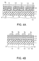
- Fig. 4A and Fig. 4B respectively show sections taken along the line A-A' and the line B-B' in Fig. 3.
- the p-type silicon layer 12 is pattern-formed in a lattice form by embedding a silicon oxide film 21 therein. Namely, regions each of which is for two transistors sharing a drain are arranged, being element-isolated in the direction of the word line WL by the silicon oxide film 21.
- element isolation in a crosswise direction may be performed by etching the silicon layer 12.
- the gate electrodes 13 are formed continuously in one direction to constitute the word lines WL.
- the source diffusion regions 15 are continuously formed in the direction of the word line WL to constitute the fixed potential lines (common source lines) SL.
- the transistor is covered with an interlayer dielectric film 23, and the bit lines BL are formed thereon.
- Each of the bit lines BL is disposed to be in contact with the drain diffusion regions 14, each of which is shared by two transistors, and intersect the word lines WL.
- the silicon layers 12, each being a bulk region of each transistor are isolated from each other at their bottom faces and side faces in the channel width direction by the oxide film, and isolated from each other in the channel lengthwise direction by a pn junction, so that a floating state is maintained.
- the operational principle of the DRAM cell composed of this N-MOS transistors utilizes the accumulation of holes which are majority carriers in the bulk region (the p-type silicon layer 12 insulatingly isolated from others) of the MOS transistor. Specifically, a large electric current is sent from the drain diffusion region 14 by operating the MOS transistor in a pentode region to generate impact ionization near the drain diffusion region 14. Excessive holes which are majority carriers produced by this impact ionization are held by the p-type silicon layer 12, and this state in which the holes are accumulated (the state in which potential is higher than in a thermal equilibrium state) is defined, for example, as data "1". The state in which a forward bias is applied to the pn junction between the drain diffusion region 14 and the p-type silicon layer 12 to emit the excessive holes in the p-type silicon layer 12 to the drain side is defined as data "0".
- the data "0" and “1” are stored as potential difference in the bulk region and stored as difference in threshold voltage of the MOS transistor. Namely, a threshold voltage Vth1 in a data "1" state in which the potential of the bulk region is high due to hole accumulation is lower than a threshold voltage Vth0 in a data "0" state.
- Vth1 a threshold voltage in which the potential of the bulk region is high due to hole accumulation
- Vth0 a data "0” state.
- a first method of reading data utilizes the event that the word line WL is given a read potential which has an intermediate value between the threshold voltages Vth0 and Vth1 of the data "0" and “1", and that a current is not passed through the memory cell storing the "0" data, while a current is passed through the memory cell storing the "1" data. More specifically, for example, the bit line BL is precharged at a predetermined potential VBL, and thereafter the word line WL is driven. Thereby, as shown in Fig. 6, in the case of the "0" data, the precharge potential VBL of the bit line does not change, while in the case of the "1" data, the precharge potential VBL lowers.
- a second read method utilizes the event that after the potential of the word line WL is raised, a current is supplied to the bit line BL, and that the increasing speed of the bit line potential is different according to the conductivity of "0" and "1".
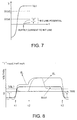
- the bit line BL is precharged at 0V, the potential of the word line WL is raised, and then a current is supplied to the bit line as shown in Fig. 7.
- a third read method is a method of reading difference in current to the bit line BL which differs according to "0" and "1" when the bit line BL is clamped at a predetermined potential.
- a current-voltage conversion circuit is necessary to read current difference, and finally potential difference is differentially amplified and a sense output is given.
- the write operation be performed by pulse write to reduce electric power consumption in the case of both "0" and "1".
- a hole current is sent from the bulk region to the drain of the selected transistor, while an electron current is sent from the drain to the bulk region, but no hole is injected into the bulk region.
- FIG. 8 to Fig. 11 show read/refresh and read/write operating waveforms when the first read method of performing data distinction by the presence or absence of electric discharge of the bit line in the selected cell is used.
- Fig. 8 and Fig. 9 respectively show read/refresh operations of the "1" data and the "0" data.
- a data holding state (a non-selected state) lasts and a negative potential is given to the word line WL.
- the word line WL is raised to a positive predetermined potential.
- the potential of the word line is set at a value between the thresholds Vth0 and Vth1 of the "0" and "1" data.
- the bit line BL precharged in advance comes to have a lower potential by electric discharge.
- the bit line potential VBL is held.
- the data "1" and "0" can be distinguished.
- the potential of the word line WL is further increased.
- a positive potential is given to the bit line BL (Fig. 8)
- a negative potential is given to the bit line BL (Fig. 9).
- the word line WL is biased in the negative direction, and the read/refresh operation is completed.
- the word line WL is held at a negative potential, and hence the bulk region thereof is held at a negative potential, whereby impact ionization does not occur.
- the word line WL is held at a negative potential as well, whereby hole emission does not occur.
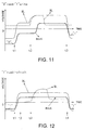
- Fig. 10 and Fig. 11 show read/write operations of the "1" data and the "0" data by the same read method.
- the read operations at the point in time t1 in Fig. 10 and Fig. 11 are the same as in Fig. 8 and Fig. 9.
- the potential of the word line WL is further increased.
- a negative potential is given to the bit line BL (Fig. 10) at the same time
- a positive potential is given to the bit line BL (Fig. 11).
- a forward bias is applied to the drain junction, and holes in the bulk region are emitted.
- impact ionization occurs around the drain, and excessive holes are injected into the bulk region and held therein.
- Fig. 12 to Fig. 15 show operating waveforms of read/refresh and read/write when the second read method of supplying a current to the bit line BL after the selection of the word line and performing data distinction by the potential increasing speed of the bit line BL is used.
- Fig. 12 and Fig. 13 respectively show read/refresh operations of the "1" data and the "0" data.
- the word line WL which is held at a negative potential is raised to a positive potential at the point in time t1.
- the potential of the word line is set at a value higher than both the thresholds Vth0 and Vth1 of the "0" and “1" data as shown in Fig. 7.
- the potential of the word line may be set at a value between the thresholds Vth0 and Vth1 of the "0" and "1” data. Then, a current is supplied to the bit line at the point in time t2.
- the word line WL is biased in the negative direction, and the read/refresh operation is completed.
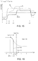
- Fig. 14 and Fig. 15 respectively show read/write operations of the "1" data and "0" data by the same read method.
- the read operations at the points in time t1 and t2 in Fig. 14 and Fig. 15 are the same as in Fig. 12 and Fig. 13.
- a negative potential is given to the bit line BL (Fig. 14)
- a positive potential is given to the bit line BL (Fig. 15).
- a forward bias is applied to the drain junction, and excessive holes in the bulk region are emitted.
- a large drain current is sent thereto to generate impact ionization around the drain, and excessive holes are injected into the bulk region and held therein.
- the DRAM cell according to the first embodiment of the present invention is composed of the simple MOS transistor having the floating bulk region which is electrically isolated from others, and the cell size of 4F 2 can be realized. Capacitive coupling from the gate electrode is used for the potential control of the floating bulk region, and, for example, back gate control from the back side of the SOI substrate is not used.
- the source diffusion region has also a fixed potential. Namely, the read/write control is performed by the word line WL and the bit line BL only, which is simple.
- data in the memory cell are basically non-destructively read out, whereby it is unnecessary to provide a sense amplifier in each bit line, which facilitates the layout of the sense amplifiers.
- since it adopts a current read method it is not affected by noise, whereby read is possible, for example, even by an open bit line system.
- the process of manufacturing the memory cell is simple.
- the SOI structure is an important technique when improvement in the performance of a logic LSI in future is considered.
- the DRAM according to the first embodiment of the present invention is very promising also when mounted together with such a logic LSI having the SOI structure. Unlike a related DRAM using a capacitor, the DRAM in the embodiment of the present invention does not need a process different from that of the logic LSI, and hence its manufacturing process is simplified.
- the DRAM having the SOI structure according to the first embodiment has an advantage that an excellent memory holding characteristic can be obtained compared with the case where a related one transistor/one capacitor-type DRAM is formed to have the SOI structure. Specifically, if the related one transistor/one capacitor-type DRAM is formed to have the SOI structure, holes are accumulated in a floating semiconductor bulk, the threshold of a transistor decreases, and thereby a subthreshold current in the transistor is increased, which deteriorates amemory holding characteristic.
- a transistor path which decreases memory charge does not exist, and hence a data holding characteristic is determined by only leakage from the pn junction, which eliminates a problem of subthreshold leakage.
- the leakage current 1 leak/area per unit area is derived from the following Formula 2.
- a value of 1 to 3 ⁇ 10 -17 A/ ⁇ m (per 1 ⁇ m in the word line direction) is hitherto reported as the leakage current from the pn junction on the SOI substrate (1995 Symp. VSLI Tech., p. 141). From this report, the above memory holding characteristic probably can be realized.
- the write time is determined by the capacitance of a cell node (gate) and a bulk current Isub.
- the bulk potential VB does not change even if the word line potential is reduced to 0 V
- non-destructive read-out is performed in principle. In order to actually guarantee the non-destructive read-out, it is necessary to confirm that:
- FIG. 17 shows an equivalent circuit used for this verification.
- the potential of the bit line BL is precharged at 0 V
- the potential Vwl of the word line WL is set at a value not less than the threshold Vth (Vth0, Vth1) of the memory cell MC at t > 0 as shown by the following Formula 5.
- the cell transistor operates in a linear region, and thus Vbl ⁇ Vwl- Vth is obtained.
- the drain current Ids of the cell transistor is derived from the following Formula 8.
- I ds k [ Vw 1 -Vth- (1/2) Vb 1] Vb 1
- Fig. 18 shows the computational result of Formula 9.
- the bit line voltage Vb10 in the "0" data and the bit line voltage Vb11 in the "1" data are shown with their respective signal voltages Vsig0 and Vsig1, and a reference bit line voltage Vbld. From this result, it is known that a signal of 100 mV can be obtained after 10 nsec from the rise of the word line.
- an MOS transistor with the same structure as the memory cell the bulk potential of which can be appropriately set is preferable. This is because it self-aligningly follows the process change or temperature change of the threshold of the memory cell. In this case, the signal quantities of the "0" and "1" data can be optimally set by selecting the bulk potential of the dummy cell.
- Is is a saturation current
- ⁇ is a coefficient between 1 and 2
- Vt is a thermal voltage
- Vt kT/q.
- Formula 11 is substituted for Formula 10 and integrated so as to obtain the following Formula 12.
- the capacitance Cgb per unit area between the gate and the bulk (p-type layer) of the SOI substrate of the cell transistor is obtained from the following Formula 14 by using the potential difference Vgb between the gate and the bulk.
- Formula 14 is derived by obtaining a thickness wp of a depletion layer which extends in the bulk, (which is derived by normalizing a thickness Wp of an actual depletion layer by ⁇ and making it dimensionless) by the following Formula 16.
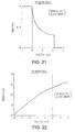
- Fig. 21 This shows the relation between the word line-bulk voltage Vgb and the capacitance Cgb of the "0" data cell in the case where the word line is a p-type polycrystalline silicon gate.
- a bulk potential change ⁇ Vb with respect to a gate voltage change ⁇ Vg is derived from the following Formula 19.
- Vg-Vg 0 ⁇ vgb vgb0 [1 +Cgb/Cj ] dVgb
- Vgb-Vgb 0 ( Vg-Vg 0)- ⁇ vgb vgb0 ( Cgb/Cj ) dVgb
- the change ⁇ Vb of the bulk voltage VB can be derived from the voltage change ⁇ Vg of the gate voltage Vwl (word line).
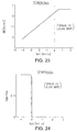
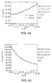
- the computational result for the "0" data cell under the same parameter conditions as those in the ,computation in Fig. 21 shown above will be shown in Fig. 22. It is known from this result that if "0" write is performed while the word line is set at 2.0 V, the bulk is set at -0.7 V, and then the wold line is decreased to -2.0 V to hold the data, for example, the bulk potential is held at -2.1 V. If the word line is further raised to 1.0 V and read is performed, the bulk increases to only about -0.9 V. Namely, as for the "0" data cell, the bulk potential in read is lower than that in write, and hence a read margin is extended by 0.2 V.
- "0" data can be written in principle up to a bulk potential of -1.0 V, but the bulk increases by 0.3 V to -0.7 V by the capacitive coupling (the coupling ratio is 18 %) of the pn junction when the bit line which has been decreased to 1.5 V in "0" write is returned to 0 V. Accordingly, in the "0" data in Fig. 22, the potential immediately after write is set at -0.7 V.
- Isub Is [exp ⁇ V /( ⁇ Vt )-1 ⁇ ]
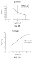
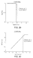
- Fig. 25 shows the result of examining a capacitance Cgb-voltage Vgb characteristic regarding the "1" data cell.
- the threshold Vth0 1 V of the "0" data can be secured
- the word line voltage is 1.5 V at the time of write, and 0.5 V at the time of read.
- the bit line level Vbl ( "1" write) at the time of "1" write is unfixed since it is fixed by a substrate current (hole current) and a write time, and a provisional set value is shown here. From the above, the advantage of the use of the p-type polycrystalline silicon gate becomes clear. In either case, the word line amplitude is 4 V. The following measures are required to lower this voltage:
- (C) will be examined in detail below, because it is a method capable of lowering the voltage of the word line amplitude without decreasing the margin of ⁇ Vth.
- the demand of (C) can be complied with by making a thickness Tsi of the silicon layer of the SOI substrate thinner than 100 nm assumed so far, and simultaneously with this or independently from this, by lowering the impurity concentration of the n-type source/drain diffusion regions.
- the former corresponds to a reduction in the pn junction capacitance Cj by a reduction in the area of the pn junction.
- the latter also reduces the junction capacitance Cj between the source/drain diffusion regions and the bulk region as well since a condition that the depletion layer extends to the n-type diffusion region side is given.
- Conditions other than Cj are the same as those in Fig. 23 and Fig, 24, and the gate electrode is p-type polycrystalline silicon.
- the silicon layer of the SOI substrate can be further thinned to approximately 30 nm, it is possible to make the voltage lower. However, if the silicon layer is excessively thinned, the silicon layer is completely depleted, which causes the danger of losing the memory function itself. Accordingly, a thickness of approximately 50 nm is appropriate for the thickness of the silicon layer.
- the maximum voltage related to the cell transistor is 3.0 V.
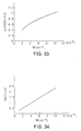
- a cell current Ids1 of the "1" write cell transistor which can be secured at the threshold difference ⁇ Vth shown in Fig. 33 and a data read time ⁇ t corresponding thereto are shown in Fig. 34 and Fig. 35 respectively.
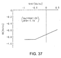
- Fig. 36 shows the result of examining a reduction in the bulk potential VB at the time of hold in the "1" data cell in relation to the threshold Vth1.
- Vth1 0.5 V or more
- the bulk potential at the time of hold increases with Vth1.
- Vth1 ⁇ 0.5 V the bulk potential is saturated at -0.93 V. This means that if the potential of the word line lowers to a value of Vth1 ⁇ 0.5 V, the capacitance Cgb is saturated as the gate oxide film capacitance Cox.
- Vth0 1.1 V
- Vth1 0.3 V
- Vwl (read) 0.7 V
- Vwl (hold) -1.7 V
- Vwl (write) 1.5 V
- Vbl -1.5 V Vbl
- 1" write 1.5 V
- Vmax 3.2 V (Vds between non-selected WL and "1" write BL)
- channel width W 0.1 ⁇ m
- Vth0 0.1 V
- Vth1 -0.7 V
- Vwl (read) 0.3 V
- Vwl (hold) -2.7 V
- channel width W 0.1 ⁇ m
- Tsi 50 nm
- the word line level Vwl (write) at the time of write is fixed with respect to the threshold Vth0 fixed by the read characteristic and the "1" write characteristic, but
- the above computation is performed for the standard DRAM cell. Actually, there are variations in the threshold of a cell transistor between lots, between wafers, in a wafer, and in a chip and variation in k caused by a manufacturing process, and also there are variation in bit line capacitance, variation in designed word line level, and the like. Moreover, it is necessary to consider coupling noise between bit lines.
- a limit can be basically set only to local variation in the chip which is a factor of the above described threshold variations. Variation in threshold accompanying variation in temperature can be completely cancelled systematically.
- the memory cell according to the embodiment of the present invention is non-destructive read-out and current read-out in principle as described above.
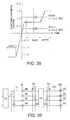
- Fig. 39 shows an example of the layout of sense amplifiers utilizing this memory cell characteristic.
- Bit lines BL and bBL which make a pair are arranged on both sides of a sense amplifier SA to form an open bit line system.
- a word line WL is activated in one of the bit lines BL and bBL
- a dummy word line DWL which selects a dummy cell DC is activated in the other.
- the dummy cell DC is composed of the same MOS transistor as the memory cell MC and gives an intermediate bulk potential between the deta "0" and "1" to its bulk region.
- bit lines BL and bBL are selected by a select gate SG and connected to one sense amplifier SA.
- Bit lines connected to some sense amplifier SA and bit lines connected to a sense amplifier SA adjacent thereto are alternately arranged.
- out of four data in the simultaneously selected four memory cells MC two data are actually detected by the sense amplifier SA, and the remaining memory cell data are read out but not sent to the sense amplifier.
- unlike an ordinary DRAM destructive read-out is not performed, and hence such a sense amplification system is possible.
- the condition 1 is required to increase the difference in threshold voltage between the "0" and “1" data by a large substrate bias effect.
- Fig. 41 shows the situation in which the relation between the bulk potential VB and the threshold Vth of the NMOS transistor differs depending on the acceptor concentration NA.
- the condition 2 is required to guarantee the data holding characteristic, in which case it is naturally desirable that the impurity concentration in the bulk region be low.
- the impurity concentration in the bulk region In order to hold data for ten seconds in the bulk region in the 0.1 ⁇ m rule DRAM generation, it is necessary to keep a leakage from the pn junction of the source and the drain at or below 3 ⁇ 10 -17 A/cm 2 .
- the electric field in the depletion layer At the above acceptor concentration demanded by the condition 1, the electric field in the depletion layer is 1.7 ⁇ 10 6 V/cm (at the time of a reverse bias of 2 V), which can not comply with the demand of the condition 2.
- Fig. 40 shows the structure of a DRAM cell MC according to a second embodiment having possibility of fulfilling the above contrary conditions 1 and 2 by contrast with Fig. 1.
- a point of difference from the cell structure in Fig. 1 lies in the bulk region composed of the p-type silicon layer 12.
- the bulk region is composed of ap-type diffusion region 12a which has a relatively low boron concentration (acceptor concentration) and touches the drain/source diffusion regions 14 and 15 and a p + -type diffusion region 12b which has a high boron concentration (acceptance concentration) and is located in the central portion in the channel length direction away from the drain/source diffusion regions 14 and 15.
- the p + -type diffusion region 12b is formed deep to reach the silicon oxide film 11 at the bottom.
- one NMOS transistor with a high threshold voltage is equivalently sandwiched between two NMOS transistors with a low threshold voltage.
- the entire threshold voltage is dominated by the p + -type diffusion region 12b in the center.
- the drain/source diffusion regions 14 and 15 each form a pn junction between the p-type diffusion region 12a with a low concentration and itself, and therefore the leakage current is smaller compared with the case where the entire bulk region is formed by the p + -type diffusion region with a high concentration.
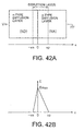
- Fig. 42A and Fig. 42B the extension of the depletion layer and the intensity distribution of an internal electric field E when a reverse bias with a voltage V is applied to the pn junction of the n-type diffusion layer (donor concentration ND) and the p-type diffusion layer (acceptor concentration NA) are found. It is supposed that the pn junction is an abrupt junction. As shown in Fig. 42A and Fig. 42B, the X-axis is defined as a direction in which the pn junction is traversed.
- ⁇ is the dielectric constant of silicon.
- Boundary conditions are shown by the following Formula 25 with the bilt-in potential as ⁇ bi.
- Formula 27 is equations for fixing six unknowns, xn, xp, A, B, C, and D.
- the following Formula 28 is obtained by solving these equations.
- xn ⁇ 2 ⁇ NA ( ⁇ bi + V )/ qND ( NA + ND ) ⁇ 1/2
- xp ⁇ 2 ⁇ ND ( ⁇ bi + V )/ qNA ( NA + ND ) ⁇ 1/2
- the field intensity distribution is as shown in Fig. 42B.
- Fig. 43A and Fig. 43B will be examined based on the above preliminary examination results.
- the junction is an abrupt junction.
- a capital letter X in place of a small letter x is used for a distance axis. It is supposed that a forward end position Xp of the depletion layer which extends to the p-type diffusion layer goes beyond a region with the low acceptor concentration na, and Xp > L is premised.
- Poisson's equations and electric field expressions are the following Formula 31 by dividing the p-type diffusion layer into the regions with the high acceptor concentration NA and the low acceptor concentration na.
- the potential and electric field of the region with the low acceptor concentration na are represented by ⁇ a and Ea respectively as against the potential ⁇ A and the electric field EA of the region with the high acceptor concentration NA.
- Formula 34 is equations for fixing eight unknowns, Xn, Xp, A, B, C, D, E, and F.
- the following Formula 35 is obtained by solving these equations.
- Xn - L ⁇ ( NA - na )/( NA + ND ) +L ⁇ ⁇ ( NA/ND )( NA-na )( ND + na )/( NA + ND ) 2 +( xn/L ) 2 ⁇ 1/2
- Xp (1/NA ) ⁇ [ ND ⁇ Xn+ ( NA-na ) ⁇ L ]
- xn in Formula 35 shows the extension of the depletion layer to the n-type diffusion layer which is already solved concerning the pn junction in Fig. 42, and it is indicated by Formula 28.
- LDD structure In order to prevent the source/drain from being depleted largely as described above, it is desirable to adopt a so-called LDD structure.
- the drain diffusion region 14 is composed of an n-type diffusion region 14a with a low donor concentration which is in contact with the channel region and an n + -type diffusion region 14b with a high donor concentration.
- the source diffusion region 15 is also composed of an n-type diffusion region 15a with a low donor concentration which is in contact with the channel region and an n + -type diffusion region 15b with a high donor concentration.
- a metal silicide film 18 is formed on the source/drain diffusion regions and the gate electrode by a salicide process.
- this LDD structure can be adopted, for example, only for the drain side connected to the bit line out of the drain and the source.
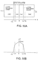
- Fig. 50A and Fig. 50B show a schematic pn junction structure and field distribution when attention is paid, for example, to the drain side junction of this cell structure by contrast with Fig. 43A and Fig. 43B.
- the n-type diffusion layer is composed of a region with a low donor concentration nd and a region with a high donor concentration ND
- the p-type diffusion layer is composed of a region with a low acceptor concentration na and a region with a high acceptor concentration NA.
- the width of the region with the low donor concentration nd is taken here as Ln and the width of the region with the low acceptor concentration na is taken as Lp.
- the regions with the high donor concentration ND and the high acceptor concentration NA respectively have concentrations fixed by resistance of bit line contact and source line contact and restrictions required in terms of a transistor characteristic.
- Xn [( ND - nd ) Ln -( NA-na ) Lp ]/( NA+ND ) + [1/( NA + ND )]( NA / ND ) 1/2 ⁇ [( NA - na )( ND + na ) Lp 2 +( ND - nd )( NA + nd ) Ln 2 + 2( NA - na )( ND - nd ) LpLn+ ( NA + ND )(2 ⁇ / q )( ⁇ bi + V )] 1/2
- Xp [( NA - na ) Lp - (ND - nd ) Ln ]/( NA + ND )+ [1/( NA+ND )]( ND / NA ) 1/2 ⁇ [( ND-nd )( NA+nd ) Ln 2 +( NA - na )( ND + na ) Lp 2 + 2( ND -
- Fig. 52 shows the result of finding the maximum electric field intensity Emax under the same conditions.
- Fig. 53 shows the extension of the depletion layer and the dimensions of respective portions in the cell structure in Fig. 49 at the above maximum field intensity on the drain region side.
- the above maximum field intensity is one third or less of that when the source/drain diffusion regions have no low concentration layer as analyzed in Fig. 43. Accordingly, as shown in Fig. 49, by forming the bulk region by the high concentration layer and the low concentration layer and making the drain and the source have the LDD structure, it becomes possible to lower the maximum field intensity to reduce the leakage current and to bring substrate bias effects into full play. Namely, the aforesaid contrary conditions 1 and 2 can be fulfilled and an excellent DRAM characteristic can be obtained.
- the memory cell MC in Fig. 49 is actually disposed in the same cell array as that explained in Fig. 3 and Fig. 4. Namely, the p-type silicon layer 12 is pattern-formed as an element region in a stripe form with its side face in the direction perpendicular to the paper surface touching an element isolation insulating film, but the explanation of the process of element isolation is omitted.
- a mask 31 having an opening in the element region is first formed on the surface of the p-type silicon layer 12 (which is the low concentration p-type region 12a), and a side wall insulating film 32 is then formed on a side wall of the opening of the mask 31.
- a silicon oxide film is deposited and patterned by RIE.
- a silicon nitride film is deposited and left as the side wall insulating film 32 by etch back. In this state, boron ion implantation is performed to form the high concentration P + -type region 12b in the p-type silicon layer 12.
- the gate insulator 16 is formed on the surface of the exposed p-type silicon layer 12. Subsequently, a polycrystalline silicon film is deposited, planarization processing is performed, and then the gate electrode 13 is buried therein.
- the mask 31 is removed by etching.
- Arsenic ion implantation is performed with the gate electrode 13 as a mask to form the low concentration drain/source diffusion regions 14a and 15a.
- a side wall insulating film 33 is formed on the side wall of the gate electrode 13.
- arsenic ion implantation is performed again to form the high concentration drain/source diffusion regions 14b and 15b.
- the metal silicide film 18 is formed on the drain/source diffusion regions 14a and 15b and the gate electrode 13 by means of the silicide process.
- the step shown in Fig. 57 is unnecessary. Namely, in the state of Fig. 56, the memory cell MC shown in Fig. 40 can be obtained.
- the p + -type region 12b can be formed while being self-aligned in the center in the channel length direction of the bulk region of the transistor.
- Fig. 58A and Fig. 58B show a plan view of one memory cell MC portion and a sectional view taken along the line A-A' regarding the one transistor/one cell structure according to a third embodiment is realized by using a pillar semiconductor layer (post type semiconductor portion).
- a so-called SGT Silicon Gate Transistor
- SGT Square Gate Transistor
- the pillar silicon layer 49 has an n + -type source diffusion region 43 formed at the bottom and a P + -type layer 46 sandwiched between p-type layers 45 in a height direction.
- An n + -type drain diffusion layer 44 is formed in the surface side of the pillar silicon layer 49.
- a gate insulator 41 is formed on the side peripheral face of the pillar silicon layer 49, and a gate electrode 42 is formed to surround the gate insulator 41.
- the gate electrodes 42 are continuously formed in one direction to constitute a word line WL.
- the SGT thus formed is covered with an interlayer dielectric film 47, and a bit line (BL) 48 is formed thereon.
- the bit line 48 is connected to the n + -type diffusion region 44.
- a bulk region is floating, and by the same write method as explained in the aforesaid embodiment, dynamic data storage can be performed by the operation of holding excessive majority carriers in the bulk region or emitting them therefrom.
- the optimization of the impurity concentrations and dimensions of the high concentration p + -type layer 46 and the low concentration p-type layers 45 disposed in the center of the bulk region makes it possible to obtain a sufficient substrate bias effect capable of increasing the difference in threshold voltage between binary data, and to decrease a leakage current to obtain an excellent data holding characteristic.
- Fig. 59A and Fig. 59B show an one transistor/one cell DRAM cell structure according to a fourth embodiment.
- Fig. 59A is a perspective view showing a bit line (BL) 58 by a virtual line to make the structure thereunder clearly understandable
- Fig. 59B is a sectional view taken along the direction of the bit line 58.
- a p-type silicon layer 52 (a part of which becomes a low concentration region 52a) isolated by a silicon oxide film 51 is formed in the form of an island on a silicon substrate 50 with its upper face and both side faces exposed.
- a gate electrode 54 is formed on the upper face and both the side faces of the silicon layer 52 via a gate insulator 53 to compose a cell transistor.
- the gate electrodes 54 are continuously patterned in one direction to constitute a word line WL.
- a high concentration p + -type region 52b is formed in the center in the channel direction of a transistor region of the silicon layer 52.
- Drain/source diffusion regions 55 and 56 have an LDD structure composed of low concentration n-type diffusion regions 55a and 56a and high concentration n + -type diffusion regions 55b and 56b.
- the transistor region is covered with an interlayer dielectric film 57, and the bit line 58 which is in contact with the drain diffusion region 55 is formed on this interlayer dielectric film 57.
- a bulk region is floating, and by the same write method as explained in the aforesaid embodiment, dynamic data storage can be performed by the operation of holding excessive majority carriers in the bulk region or emitting them therefrom.
- the optimization of the impurity concentrations and dimensions of the high concentration p + -type regions 52b and the low concentration p-type regions 52a disposed in the center of the bulk region makes it possible to obtain a sufficient substrate bias effect capable of increasing the difference in threshold voltage between binary data, and to decrease a leakage current to obtain an excellent data holding characteristic.
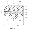
- Fig 60A is a diagram showing the layout of the memory cell array
- Fig. 60B is a sectional view taken along the line I-I' in Fig. 60A
- Fig, 60C is also a sectional view taken along II-II' therein.
- the memory cell array has an SOI substrate, which is composed of a silicon substrate 101, an insulating film 102 which is formed on the silicon substrate 101 and which is a silicon oxide film and so on, and a p-type silicon layer 103 which is formed thereon.
- An element isolation insulating film 109 is embedded in the silicon layer 103 by using an STI method, so that the silicon layer 103 is divided in a given pitch in the direction of the word line WL into element forming regions in long stripes form in the direction of the bit line BL.
- the transistors are arranged in a matrix form in the silicon layer 103 element-isolated in this way. That is, gate electrodes 105 are pattern-formed continuously as the word lines WL on the silicon layer 103 via gate insulators 104. The upper face and both side faces of each of the gate electrodes 105 are covered with a silicon nitride film 106 as a protection film which has a large etching selective ratio to interlayer dielectric films 110 and 115 formed later.
- Source/drain diffusion regions 107 and 108 are formed by a self-alignment process using the gate electrodes 105. The source/drain diffusion regions 107 and 108 are formed deep to reach the insulating film 102 at the bottom of the silicon layer 103.
- the surface formed the transistors is covered with the interlayer dielectric film 110, which is a silicon oxide film or the like and which is flattened.
- Contact holes 111 for the source diffusion region 107 are formed in the interlayer dielectric film 110 in stripes form which continue in the direction of the word line WL, and a source wiring portion 112, which is a polysilicon film, WSi film or the like, is embedded in each of the contact holes 111.
- the interlayer dielectric film 115 which is a silicon oxide film and so on, is formed on the interlayer dielectric film 110 embedded the source wiring portion 112 and which is flattened.
- Contact holes 116 for the drain diffusion regions 108 are formed in the interlayer dielectric film 115, and a contact plug 117 of a polysilicon film and the like is embedded in each of the contact holes 116.
- bit lines 118 (BL) are formed on the interlayer dielectric film 115 so as to commonly connect the contact plugs 117, and the bit lines 118 cross the word lines WL.
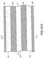
- Figs. 61A, 61B and 61C are a plan view and sectional views taken along I-I' and II-II' in a stage where the element isolation insulating film 109 is formed in the p-type silicon layer 103 of the SOI substrate. For example, this is obtained by etching the silicon layer 103 with RIE so as to form element isolation grooves and embedding the element isolation insulating film 109 in the element isolation grooves. As a result, the silicon layer 103 is divided into the element forming regions in a plurality of stripes continuing in the direction of the bit line BL.
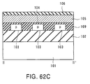
- Figs. 62A, 62B and 62C are a plan view and sectional views taken along I-I' and II-II' in a stage where the transistors are formed. That is, the gate electrodes 105 are pattern-formed via the gate insulator 104 as the continuously word lines WL. The upper face and both side faces of each of the gate electrodes 105 are covered with the silicon nitride film 106. Specifically, this gate electrode protecting structure is obtained through steps of patterning a laminated film of a polysilicon film and a silicon nitride film and forming a silicon nitride film on both the side faces thereof. Then, an ion implantation is performed with the gate electrodes 105 being used as a mask, so that the source/drain diffusion regions 107 and 108 are formed.
- Figs. 63A and 63B are a plan view and a sectional view taken along I-I' in a stage where the substrate is covered with the interlayer dielectric film 110 and the source wiring portions 112 are embedded in the interlayer dielectric film 110. That is, the interlayer dielectric film 110, which is a silicon oxide film and so on, is formed flatly and the contact holes 111, which are in parallel with the word lines WL and in stripes, are formed on the source diffusion regions 107 by RIE. Then, a polysilicon film is formed and etched-back, so that the source wiring portions 112 embedded in the contact holes 111 are formed.
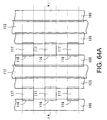
- Figs. 64A and 64B are a plan view and a sectional view taken along I-I' in a stage where the interlayer dielectric film 115 is formed on the interlayer film 110 in which the source wiring portions 112 are formed and then the contact plugs 117 are embedded in the interlayer dielectric film 115.
- the interlayer dielectric film 115 which is a silicon oxide film and so on, is formed flatly and the contact holes 116 are formed therein on the drain diffusion regions 108 by RIE.
- a polysilicon film is formed and etched-back, so that the contact plugs 117 embedded in the contact holes 116 are formed.
- the bit lines 118 are formed on the interlayer dielectric film 115 so as to commonly connect the contact plugs 117.
- the DRAM cell array which has 4F 2 cell area is obtained as shown by one dotted chain line in Fig. 60A, and the word lines WL and the bit lines BL are formed with pitches of the minimum feature size F.
- the source diffusion regions 107 are formed discretely in the direction of the word line WL.
- the source wiring portions 112 are formed so as to commonly connect the source diffusion regions 107, so that the common source lines with low resistance are obtained.
- Both the contact holes 111 for the source wiring portions 112 and the contact holes 116 for the bit line contact plugs 117 are formed by self-alignment processes using the gate electrodes 105 protected by the silicon nitride film 106. Therefore, it is possible to make the contact holes without an influence of mask matching deviation by setting the width of mask hole in more than F in RIE of a contact hole opening process.
- the contact holes 116 are formed only on the drain diffusion regions 108.
- contact holes 116b for the bit lines may be continuously formed along the direction of the word line WL in stripes in the same way as the contact holes 111 for the source diffusion regions 107.
- contact plugs 117 are also embedded in the contact holes 116b in stripes, it is necessary that the contact plugs 117 only under the bit lines BL remain finally.
- it can be realized by pattern-forming the bit lines BL and etching the contact plugs 117 by using the bit lines BL as a mask.
- an interlayer dielectric film 201 which is a silicon oxide film and so on is formed on the substrate in which elements are formed, and the interlayer dielectric film 201 is etched-back to be flat.
- the silicon nitride film 106 covering the gate electrode 105 is used as a stopper in an etching process, so that the interlayer dielectric film 201 is embedded in aperture between the gates.
- contact holes for the source/drain diffusion regions 107 and 108 are opened in the interlayer dielectric film 201, and contact plugs 202 and 203 are embedded in the contact holes by forming a polysilicon film and etching it back, respectively. If a mask which has openings in stripes continuing along the direction of the bit line BL is used, contact holes are formed between gate electrodes 105 by self-alignment. However, contact plugs 202 on the source diffusion regions 107 may continue in parallel with the word lines WL as in the case of the above-mentioned embodiment.
- source wiring portions 204 are formed so as to commonly connect the contact plugs 202 on the source diffusion regions 107.
- the upper face and both side faces of each of the source wiring portions 204 are covered with a silicon nitride film as a protection film.
- this protection structure is obtained by patterning a laminate film of a polysilicon film and a nitride silicon film to form source wiring portions 204 and then forming the silicon nitride film 205 on both side faces thereof.
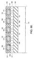
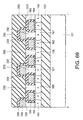
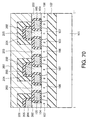
- an interlayer dielectric film 206 which is a silicon oxide film and so on, is formed again and flattened. Grooves and contact holes for embedding the bit lines are formed in the interlayer dielectric film 206 using Dual Damascene Method, and bit lines 207 are embedded therein as shown in Fig. 70.
- the bit line contact with low resistance can be obtained without an influence of mask alignment deviation.
- each of the element formed regions does not continue in the direction of the word line WL.
- Fig. 71 it is possible to define the element forming regions continuously in the direction of the word line WL at the position of the source diffusion region.
- the source diffusion regions are formed continuously in the direction of the word line and constitute common source lines themselves. Even in this case, it is effective for realizing the common source lines with low resistance to form the source wiring portions 112 in the same way as the above-mentioned embodiments.
- the present invention is not limited to the above embodiments.
- the N-channel MOS transistor formed in the p-type silicon layer is used in the embodiments, but even if a P-channel MOS transistor formed in an n-type silicon layer is used as a memory cell, dynamic storage is possible by the same principle.
- amajority carrier is an electron, and accumulation and emission of electrons in/from the bulk region is utilized.
- the SOI substrate is used in the embodiments, it is possible to form a memory cell of the same principle by an MOS transistor using a semiconductor layer which gets floating by pn junction isolation.
- a semiconductor memory device in which a simple transistor structure is used as a memory cell, enabling dynamic storage of binary data by a small number of signal lines can be provided.
Landscapes
- Engineering & Computer Science (AREA)
- Microelectronics & Electronic Packaging (AREA)
- Computer Hardware Design (AREA)
- Semiconductor Memories (AREA)
- Dram (AREA)
Applications Claiming Priority (6)
| Application Number | Priority Date | Filing Date | Title |
|---|---|---|---|
| JP2000247735 | 2000-08-17 | ||
| JP2000247735 | 2000-08-17 | ||
| JP2000389106 | 2000-12-21 | ||
| JP2000389106 | 2000-12-21 | ||
| JP2001180633 | 2001-06-14 | ||
| JP2001180633 | 2001-06-14 |
Publications (2)
| Publication Number | Publication Date |
|---|---|
| EP1180799A2 true EP1180799A2 (de) | 2002-02-20 |
| EP1180799A3 EP1180799A3 (de) | 2005-09-28 |
Family
ID=27344368
Family Applications (1)
| Application Number | Title | Priority Date | Filing Date |
|---|---|---|---|
| EP01119605A Withdrawn EP1180799A3 (de) | 2000-08-17 | 2001-08-17 | Halbleiter-Speicherbauteil und Verfahren zur Herstellung desselben |
Country Status (2)
| Country | Link |
|---|---|
| US (5) | US6621725B2 (de) |
| EP (1) | EP1180799A3 (de) |
Cited By (27)
| Publication number | Priority date | Publication date | Assignee | Title |
|---|---|---|---|---|
| EP1351307A1 (de) * | 2002-03-28 | 2003-10-08 | Innovative Silicon SA | Verfahren zum Ansteuern eines Halbleiterbauteils |
| EP1355357A1 (de) * | 2002-04-18 | 2003-10-22 | Innovative Silicon SA | Elektrisches Ladungsträger-Halbleiterbauelement |
| WO2002103703A3 (en) * | 2001-06-18 | 2004-01-29 | Innovative Silicon Sa | Semiconductor device |
| WO2005008778A1 (en) * | 2003-07-22 | 2005-01-27 | Innovative Silicon S.A. | Integrated circuit device, and method of fabricating same |
| US6912150B2 (en) | 2003-05-13 | 2005-06-28 | Lionel Portman | Reference current generator, and method of programming, adjusting and/or operating same |
| WO2007028583A1 (en) * | 2005-09-07 | 2007-03-15 | Innovative Silicon S.A. | Memory cell and memory cell array having an electrically floating body transistor, and methods of operating same |
| US7242608B2 (en) | 2000-08-17 | 2007-07-10 | Kabushiki Kaisha Toshiba | Semiconductor memory device having a floating storage bulk region capable of holding/emitting excessive majority carriers |
| US7923766B2 (en) | 2008-06-12 | 2011-04-12 | Elpida Memory, Inc | Semiconductor device including capacitorless RAM |
| US8492209B2 (en) | 2007-01-26 | 2013-07-23 | Micron Technology, Inc. | Semiconductor device with electrically floating body |
| US8659956B2 (en) | 2007-05-30 | 2014-02-25 | Micron Technology, Inc. | Integrated circuit having voltage generation circuitry for memory cell array, and method of operating and/or controlling same |
| US8699289B2 (en) | 2009-11-24 | 2014-04-15 | Micron Technology, Inc. | Techniques for reducing disturbance in a semiconductor memory device |
| US8773933B2 (en) | 2012-03-16 | 2014-07-08 | Micron Technology, Inc. | Techniques for accessing memory cells |
| US8792276B2 (en) | 2009-04-30 | 2014-07-29 | Micron Technology, Inc. | Semiconductor device with floating gate and electrically floating body |
| US8797819B2 (en) | 2007-09-17 | 2014-08-05 | Micron Technology, Inc. | Refreshing data of memory cells with electrically floating body transistors |
| US8817534B2 (en) | 2009-07-10 | 2014-08-26 | Micron Technology, Inc. | Techniques for providing a semiconductor memory device |
| US8861247B2 (en) | 2009-04-27 | 2014-10-14 | Micron Technology, Inc. | Techniques for providing a direct injection semiconductor memory device |
| US8947965B2 (en) | 2009-07-27 | 2015-02-03 | Micron Technology Inc. | Techniques for providing a direct injection semiconductor memory device |
| US8964479B2 (en) | 2010-03-04 | 2015-02-24 | Micron Technology, Inc. | Techniques for sensing a semiconductor memory device |
| US8982633B2 (en) | 2009-05-22 | 2015-03-17 | Micron Technology, Inc. | Techniques for providing a direct injection semiconductor memory device |
| US9019759B2 (en) | 2010-03-15 | 2015-04-28 | Micron Technology, Inc. | Techniques for providing a semiconductor memory device |
| US9064730B2 (en) | 2009-03-04 | 2015-06-23 | Micron Technology, Inc. | Techniques for forming a contact to a buried diffusion layer in a semiconductor memory device |
| US9093311B2 (en) | 2009-03-31 | 2015-07-28 | Micron Technology, Inc. | Techniques for providing a semiconductor memory device |
| US9142264B2 (en) | 2010-05-06 | 2015-09-22 | Micron Technology, Inc. | Techniques for refreshing a semiconductor memory device |
| US9263133B2 (en) | 2011-05-17 | 2016-02-16 | Micron Technology, Inc. | Techniques for providing a semiconductor memory device |
| US9276000B2 (en) | 2007-03-29 | 2016-03-01 | Micron Technology, Inc. | Manufacturing process for zero-capacitor random access memory circuits |
| US9553186B2 (en) | 2008-09-25 | 2017-01-24 | Micron Technology, Inc. | Recessed gate silicon-on-insulator floating body device with self-aligned lateral isolation |
| US10304837B2 (en) | 2007-11-29 | 2019-05-28 | Ovonyx Memory Technology, Llc | Integrated circuit having memory cell array including barriers, and method of manufacturing same |
Families Citing this family (156)
| Publication number | Priority date | Publication date | Assignee | Title |
|---|---|---|---|---|
| JP2003031693A (ja) * | 2001-07-19 | 2003-01-31 | Toshiba Corp | 半導体メモリ装置 |
| JP4091304B2 (ja) * | 2002-01-07 | 2008-05-28 | セイコーインスツル株式会社 | 半導体集積回路の製造方法及び半導体集積回路 |
| JP2003273245A (ja) * | 2002-03-15 | 2003-09-26 | Hitachi Ltd | 半導体記憶装置 |
| EP1355316B1 (de) * | 2002-04-18 | 2007-02-21 | Innovative Silicon SA | Datenspeichergerät sowie Verfahren zum Auffrischen der auf einem solchen Gerät gespeicherten Daten |
| EP1357603A3 (de) * | 2002-04-18 | 2004-01-14 | Innovative Silicon SA | Halbleiterbauelement |
| JP2004022093A (ja) * | 2002-06-18 | 2004-01-22 | Toshiba Corp | 半導体記憶装置 |
| JP3962638B2 (ja) * | 2002-06-18 | 2007-08-22 | 株式会社東芝 | 半導体記憶装置、及び、半導体装置 |
| JP4044401B2 (ja) * | 2002-09-11 | 2008-02-06 | 株式会社東芝 | 半導体記憶装置 |
| JP2004111643A (ja) * | 2002-09-18 | 2004-04-08 | Toshiba Corp | 半導体記憶装置、及び、その制御方法 |
| US6861689B2 (en) * | 2002-11-08 | 2005-03-01 | Freescale Semiconductor, Inc. | One transistor DRAM cell structure and method for forming |
| US6714436B1 (en) | 2003-03-20 | 2004-03-30 | Motorola, Inc. | Write operation for capacitorless RAM |
| US20040228168A1 (en) * | 2003-05-13 | 2004-11-18 | Richard Ferrant | Semiconductor memory device and method of operating same |
| US7085153B2 (en) * | 2003-05-13 | 2006-08-01 | Innovative Silicon S.A. | Semiconductor memory cell, array, architecture and device, and method of operating same |
| JP4282388B2 (ja) * | 2003-06-30 | 2009-06-17 | 株式会社東芝 | 半導体記憶装置 |
| JP3933608B2 (ja) * | 2003-06-30 | 2007-06-20 | 株式会社東芝 | 半導体記憶装置及び半導体集積回路 |
| US7184298B2 (en) * | 2003-09-24 | 2007-02-27 | Innovative Silicon S.A. | Low power programming technique for a floating body memory transistor, memory cell, and memory array |
| JP4443886B2 (ja) * | 2003-09-30 | 2010-03-31 | 株式会社東芝 | 半導体記憶装置 |
| JP4044510B2 (ja) | 2003-10-30 | 2008-02-06 | 株式会社東芝 | 半導体集積回路装置 |
| JP4559728B2 (ja) * | 2003-12-26 | 2010-10-13 | 株式会社東芝 | 半導体記憶装置 |
| JP4028499B2 (ja) * | 2004-03-01 | 2007-12-26 | 株式会社東芝 | 半導体記憶装置 |
| US7476945B2 (en) * | 2004-03-17 | 2009-01-13 | Sanyo Electric Co., Ltd. | Memory having reduced memory cell size |
| JP4032039B2 (ja) * | 2004-04-06 | 2008-01-16 | 株式会社東芝 | 半導体記憶装置 |
| JP4110115B2 (ja) * | 2004-04-15 | 2008-07-02 | 株式会社東芝 | 半導体記憶装置 |
| JP4149961B2 (ja) * | 2004-05-20 | 2008-09-17 | 株式会社東芝 | 半導体記憶装置 |
| JP2006012991A (ja) * | 2004-06-23 | 2006-01-12 | Toshiba Corp | 半導体記憶装置 |
| JP4358056B2 (ja) | 2004-07-28 | 2009-11-04 | 東芝メモリシステムズ株式会社 | 半導体メモリ |
| JP2006073062A (ja) * | 2004-08-31 | 2006-03-16 | Toshiba Corp | 半導体記憶装置 |
| JP4195427B2 (ja) * | 2004-08-31 | 2008-12-10 | 株式会社東芝 | 半導体記憶装置 |
| JP4660163B2 (ja) * | 2004-10-29 | 2011-03-30 | 東芝メモリシステムズ株式会社 | 半導体記憶装置 |
| US7476939B2 (en) * | 2004-11-04 | 2009-01-13 | Innovative Silicon Isi Sa | Memory cell having an electrically floating body transistor and programming technique therefor |
| US7251164B2 (en) * | 2004-11-10 | 2007-07-31 | Innovative Silicon S.A. | Circuitry for and method of improving statistical distribution of integrated circuits |
| JP4081071B2 (ja) * | 2004-11-26 | 2008-04-23 | 株式会社東芝 | 半導体記憶装置とその製造方法 |
| JP2006164447A (ja) * | 2004-12-09 | 2006-06-22 | Toshiba Corp | 半導体記憶装置 |
| US7301838B2 (en) | 2004-12-13 | 2007-11-27 | Innovative Silicon S.A. | Sense amplifier circuitry and architecture to write data into and/or read from memory cells |
| US7301803B2 (en) * | 2004-12-22 | 2007-11-27 | Innovative Silicon S.A. | Bipolar reading technique for a memory cell having an electrically floating body transistor |
| JP4040622B2 (ja) * | 2004-12-24 | 2008-01-30 | 株式会社東芝 | 半導体記憶装置 |
| JP4469744B2 (ja) * | 2005-03-18 | 2010-05-26 | 株式会社東芝 | 半導体記憶装置および半導体記憶装置の駆動方法 |
| JP2006269535A (ja) * | 2005-03-22 | 2006-10-05 | Toshiba Corp | 半導体記憶装置および半導体記憶装置の製造方法 |
| US7230846B2 (en) * | 2005-06-14 | 2007-06-12 | Intel Corporation | Purge-based floating body memory |
| US20070023833A1 (en) * | 2005-07-28 | 2007-02-01 | Serguei Okhonin | Method for reading a memory cell having an electrically floating body transistor, and memory cell and array implementing same |
| JP4664777B2 (ja) * | 2005-09-07 | 2011-04-06 | 株式会社東芝 | 半導体装置 |
| US7355916B2 (en) | 2005-09-19 | 2008-04-08 | Innovative Silicon S.A. | Method and circuitry to generate a reference current for reading a memory cell, and device implementing same |
| US20070085140A1 (en) * | 2005-10-19 | 2007-04-19 | Cedric Bassin | One transistor memory cell having strained electrically floating body region, and method of operating same |
| JP4373972B2 (ja) * | 2005-11-14 | 2009-11-25 | 東芝メモリシステムズ株式会社 | 半導体記憶装置 |
| US7683430B2 (en) * | 2005-12-19 | 2010-03-23 | Innovative Silicon Isi Sa | Electrically floating body memory cell and array, and method of operating or controlling same |
| KR100675300B1 (ko) * | 2006-01-06 | 2007-01-29 | 삼성전자주식회사 | 캐패시터가 없는 동적 메모리 셀을 구비한 반도체 메모리장치 및 이 장치의 데이터 라이트 및 리드 방법 |
| JP4373986B2 (ja) * | 2006-02-16 | 2009-11-25 | 株式会社東芝 | 半導体記憶装置 |
| US7542345B2 (en) * | 2006-02-16 | 2009-06-02 | Innovative Silicon Isi Sa | Multi-bit memory cell having electrically floating body transistor, and method of programming and reading same |
| US7492632B2 (en) | 2006-04-07 | 2009-02-17 | Innovative Silicon Isi Sa | Memory array having a programmable word length, and method of operating same |
| JP4406413B2 (ja) * | 2006-04-18 | 2010-01-27 | 株式会社東芝 | 半導体記憶装置及びその読み出し方法 |
| US7606098B2 (en) | 2006-04-18 | 2009-10-20 | Innovative Silicon Isi Sa | Semiconductor memory array architecture with grouped memory cells, and method of controlling same |
| US7933142B2 (en) * | 2006-05-02 | 2011-04-26 | Micron Technology, Inc. | Semiconductor memory cell and array using punch-through to program and read same |
| US8069377B2 (en) | 2006-06-26 | 2011-11-29 | Micron Technology, Inc. | Integrated circuit having memory array including ECC and column redundancy and method of operating the same |
| US7542340B2 (en) * | 2006-07-11 | 2009-06-02 | Innovative Silicon Isi Sa | Integrated circuit including memory array having a segmented bit line architecture and method of controlling and/or operating same |
| US7408813B2 (en) * | 2006-08-03 | 2008-08-05 | Micron Technology, Inc. | Block erase for volatile memory |
| JP2008117489A (ja) * | 2006-11-07 | 2008-05-22 | Toshiba Corp | 半導体記憶装置 |
| JP5019436B2 (ja) * | 2007-02-22 | 2012-09-05 | ルネサスエレクトロニクス株式会社 | 半導体集積回路 |
| US8085594B2 (en) | 2007-06-01 | 2011-12-27 | Micron Technology, Inc. | Reading technique for memory cell with electrically floating body transistor |
| US7969808B2 (en) * | 2007-07-20 | 2011-06-28 | Samsung Electronics Co., Ltd. | Memory cell structures, memory arrays, memory devices, memory controllers, and memory systems, and methods of manufacturing and operating the same |
| KR20090116088A (ko) * | 2008-05-06 | 2009-11-11 | 삼성전자주식회사 | 정보 유지 능력과 동작 특성이 향상된 커패시터리스 1t반도체 메모리 소자 |
| KR101308048B1 (ko) * | 2007-10-10 | 2013-09-12 | 삼성전자주식회사 | 반도체 메모리 장치 |
| US8349662B2 (en) | 2007-12-11 | 2013-01-08 | Micron Technology, Inc. | Integrated circuit having memory cell array, and method of manufacturing same |
| JP2009152407A (ja) * | 2007-12-20 | 2009-07-09 | Toshiba Corp | 半導体記憶装置 |
| KR20090075063A (ko) * | 2008-01-03 | 2009-07-08 | 삼성전자주식회사 | 플로팅 바디 트랜지스터를 이용한 동적 메모리 셀을 가지는메모리 셀 어레이를 구비하는 반도체 메모리 장치 및 이장치의 동작 방법 |
| US8014195B2 (en) | 2008-02-06 | 2011-09-06 | Micron Technology, Inc. | Single transistor memory cell |
| US8189376B2 (en) | 2008-02-08 | 2012-05-29 | Micron Technology, Inc. | Integrated circuit having memory cells including gate material having high work function, and method of manufacturing same |
| US7772649B2 (en) * | 2008-02-25 | 2010-08-10 | International Business Machines Corporation | SOI field effect transistor with a back gate for modulating a floating body |
| US7957206B2 (en) | 2008-04-04 | 2011-06-07 | Micron Technology, Inc. | Read circuitry for an integrated circuit having memory cells and/or a memory cell array, and method of operating same |
| KR101000472B1 (ko) * | 2008-05-07 | 2010-12-14 | 주식회사 하이닉스반도체 | Soi 소자 및 그의 제조방법 |
| KR101442175B1 (ko) * | 2008-05-23 | 2014-09-18 | 삼성전자주식회사 | 반도체 메모리 장치 및 이 장치의 메모리 셀 어레이의 배치방법 |
| CN101621030B (zh) * | 2008-07-02 | 2011-01-12 | 中芯国际集成电路制造(上海)有限公司 | 具有多晶硅接触的自对准mos结构 |
| JP2010034191A (ja) * | 2008-07-28 | 2010-02-12 | Toshiba Corp | 半導体記憶装置とその製造方法 |
| US7933140B2 (en) | 2008-10-02 | 2011-04-26 | Micron Technology, Inc. | Techniques for reducing a voltage swing |
| KR20100038975A (ko) * | 2008-10-07 | 2010-04-15 | 삼성전자주식회사 | 커패시터 없는 디램 소자 |
| US7924630B2 (en) | 2008-10-15 | 2011-04-12 | Micron Technology, Inc. | Techniques for simultaneously driving a plurality of source lines |
| US8223574B2 (en) | 2008-11-05 | 2012-07-17 | Micron Technology, Inc. | Techniques for block refreshing a semiconductor memory device |
| US8213226B2 (en) * | 2008-12-05 | 2012-07-03 | Micron Technology, Inc. | Vertical transistor memory cell and array |
| KR20100070158A (ko) * | 2008-12-17 | 2010-06-25 | 삼성전자주식회사 | 커패시터가 없는 동작 메모리 셀을 구비한 반도체 메모리 장치 및 이 장치의 동작 방법 |
| KR101442177B1 (ko) * | 2008-12-18 | 2014-09-18 | 삼성전자주식회사 | 커패시터 없는 1-트랜지스터 메모리 셀을 갖는 반도체소자의 제조방법들 |
| JP2010157283A (ja) * | 2008-12-26 | 2010-07-15 | Toshiba Corp | 半導体記憶装置 |
| JP2010160865A (ja) * | 2009-01-09 | 2010-07-22 | Toshiba Corp | 半導体記憶装置および半導体記憶装置の駆動方法 |
| US8319294B2 (en) | 2009-02-18 | 2012-11-27 | Micron Technology, Inc. | Techniques for providing a source line plane |
| JP2010218629A (ja) * | 2009-03-17 | 2010-09-30 | Toshiba Corp | 半導体記憶装置 |
| US8148780B2 (en) | 2009-03-24 | 2012-04-03 | Micron Technology, Inc. | Devices and systems relating to a memory cell having a floating body |
| US7929343B2 (en) * | 2009-04-07 | 2011-04-19 | Micron Technology, Inc. | Methods, devices, and systems relating to memory cells having a floating body |
| FR2944641B1 (fr) * | 2009-04-15 | 2011-04-29 | Centre Nat Rech Scient | Point memoire ram a un transistor. |
| JP4945609B2 (ja) * | 2009-09-02 | 2012-06-06 | 株式会社東芝 | 半導体集積回路装置 |
| US8199595B2 (en) | 2009-09-04 | 2012-06-12 | Micron Technology, Inc. | Techniques for sensing a semiconductor memory device |
| US8310893B2 (en) | 2009-12-16 | 2012-11-13 | Micron Technology, Inc. | Techniques for reducing impact of array disturbs in a semiconductor memory device |
| JP2011155071A (ja) * | 2010-01-26 | 2011-08-11 | Toshiba Corp | 半導体記憶装置 |
| US8416636B2 (en) * | 2010-02-12 | 2013-04-09 | Micron Technology, Inc. | Techniques for controlling a semiconductor memory device |
| US8507966B2 (en) | 2010-03-02 | 2013-08-13 | Micron Technology, Inc. | Semiconductor cells, arrays, devices and systems having a buried conductive line and methods for forming the same |
| US9608119B2 (en) | 2010-03-02 | 2017-03-28 | Micron Technology, Inc. | Semiconductor-metal-on-insulator structures, methods of forming such structures, and semiconductor devices including such structures |
| US9646869B2 (en) | 2010-03-02 | 2017-05-09 | Micron Technology, Inc. | Semiconductor devices including a diode structure over a conductive strap and methods of forming such semiconductor devices |
| US8288795B2 (en) | 2010-03-02 | 2012-10-16 | Micron Technology, Inc. | Thyristor based memory cells, devices and systems including the same and methods for forming the same |
| US8411513B2 (en) | 2010-03-04 | 2013-04-02 | Micron Technology, Inc. | Techniques for providing a semiconductor memory device having hierarchical bit lines |
| US8369177B2 (en) | 2010-03-05 | 2013-02-05 | Micron Technology, Inc. | Techniques for reading from and/or writing to a semiconductor memory device |
| JP2011222105A (ja) | 2010-04-14 | 2011-11-04 | Elpida Memory Inc | 半導体装置 |
| JP2012033575A (ja) * | 2010-07-28 | 2012-02-16 | Sumitomo Electric Ind Ltd | 半導体装置 |
| JP5588816B2 (ja) * | 2010-10-12 | 2014-09-10 | 株式会社日立製作所 | 半導体記憶装置 |
| US8598621B2 (en) | 2011-02-11 | 2013-12-03 | Micron Technology, Inc. | Memory cells, memory arrays, methods of forming memory cells, and methods of forming a shared doped semiconductor region of a vertically oriented thyristor and a vertically oriented access transistor |
| US8952418B2 (en) | 2011-03-01 | 2015-02-10 | Micron Technology, Inc. | Gated bipolar junction transistors |
| US8519431B2 (en) | 2011-03-08 | 2013-08-27 | Micron Technology, Inc. | Thyristors |
| KR20120118785A (ko) * | 2011-04-19 | 2012-10-29 | 에스케이하이닉스 주식회사 | 플로팅 바디 효과를 제어하기 위한 컨트롤 비트라인을 갖는 반도체 소자, 그 반도체 소자를 갖는 모듈 및 시스템 |
| US9559216B2 (en) | 2011-06-06 | 2017-01-31 | Micron Technology, Inc. | Semiconductor memory device and method for biasing same |
| US8772848B2 (en) | 2011-07-26 | 2014-07-08 | Micron Technology, Inc. | Circuit structures, memory circuitry, and methods |
| JP2013102136A (ja) * | 2011-10-14 | 2013-05-23 | Elpida Memory Inc | 半導体装置およびその製造方法 |
| US9466493B2 (en) | 2013-07-11 | 2016-10-11 | Taiwan Semiconductor Manufacturing Co., Ltd. | Sense amplifier layout for FinFET technology |
| US9508854B2 (en) | 2013-12-06 | 2016-11-29 | Ecole Polytechnique Federale De Lausanne (Epfl) | Single field effect transistor capacitor-less memory device and method of operating the same |
| US10121553B2 (en) | 2015-09-30 | 2018-11-06 | Sunrise Memory Corporation | Capacitive-coupled non-volatile thin-film transistor NOR strings in three-dimensional arrays |
| US9892800B2 (en) | 2015-09-30 | 2018-02-13 | Sunrise Memory Corporation | Multi-gate NOR flash thin-film transistor strings arranged in stacked horizontal active strips with vertical control gates |
| US11120884B2 (en) | 2015-09-30 | 2021-09-14 | Sunrise Memory Corporation | Implementing logic function and generating analog signals using NOR memory strings |
| US9842651B2 (en) | 2015-11-25 | 2017-12-12 | Sunrise Memory Corporation | Three-dimensional vertical NOR flash thin film transistor strings |
| US12537057B2 (en) | 2015-09-30 | 2026-01-27 | Sunrise Memory Corporation | Three-dimensional vertical nor flash thin film transistor strings |
| EP3913631A1 (de) * | 2015-11-25 | 2021-11-24 | Sunrise Memory Corporation | Dreidimensionale vertikale oder nicht dünnschichtige flash-transistorketten |
| CN108496073B (zh) * | 2015-12-17 | 2022-01-18 | 奥卢大学 | 用于产生电离的设备、光学测量设备和测量方法 |
| CN105405846B (zh) * | 2015-12-31 | 2018-04-17 | 上海华虹宏力半导体制造有限公司 | 动态随机存储器单元结构 |
| US9875976B2 (en) * | 2015-12-31 | 2018-01-23 | Taiwan Semiconductor Manufacturing Company Ltd. | Switching device |
| US10692874B2 (en) | 2017-06-20 | 2020-06-23 | Sunrise Memory Corporation | 3-dimensional NOR string arrays in segmented stacks |
| US10608011B2 (en) | 2017-06-20 | 2020-03-31 | Sunrise Memory Corporation | 3-dimensional NOR memory array architecture and methods for fabrication thereof |
| US10608008B2 (en) | 2017-06-20 | 2020-03-31 | Sunrise Memory Corporation | 3-dimensional nor strings with segmented shared source regions |
| US11180861B2 (en) | 2017-06-20 | 2021-11-23 | Sunrise Memory Corporation | 3-dimensional NOR string arrays in segmented stacks |
| US10896916B2 (en) | 2017-11-17 | 2021-01-19 | Sunrise Memory Corporation | Reverse memory cell |
| CN111742368B (zh) | 2017-12-28 | 2022-09-13 | 日升存储公司 | 具有很细节距的三维nor存储器阵列:装置和方法 |
| US10475812B2 (en) | 2018-02-02 | 2019-11-12 | Sunrise Memory Corporation | Three-dimensional vertical NOR flash thin-film transistor strings |
| US11751391B2 (en) | 2018-07-12 | 2023-09-05 | Sunrise Memory Corporation | Methods for fabricating a 3-dimensional memory structure of nor memory strings |
| US11069696B2 (en) | 2018-07-12 | 2021-07-20 | Sunrise Memory Corporation | Device structure for a 3-dimensional NOR memory array and methods for improved erase operations applied thereto |
| US10741581B2 (en) | 2018-07-12 | 2020-08-11 | Sunrise Memory Corporation | Fabrication method for a 3-dimensional NOR memory array |
| TWI713195B (zh) | 2018-09-24 | 2020-12-11 | 美商森恩萊斯記憶體公司 | 三維nor記憶電路製程中之晶圓接合及其形成之積體電路 |
| CN113169041B (zh) | 2018-12-07 | 2024-04-09 | 日升存储公司 | 形成多层垂直nor型存储器串阵列的方法 |
| JP7425069B2 (ja) | 2019-01-30 | 2024-01-30 | サンライズ メモリー コーポレイション | 基板接合を用いた高帯域幅・大容量メモリ組み込み型電子デバイス |
| JP7655853B2 (ja) | 2019-02-11 | 2025-04-02 | サンライズ メモリー コーポレイション | 垂直型薄膜トランジスタ、及び、垂直型薄膜トランジスタの、3次元メモリアレイのためのビット線コネクタとしての応用メモリ回路方法 |
| US11217600B2 (en) | 2019-07-09 | 2022-01-04 | Sunrise Memory Corporation | Process for a 3-dimensional array of horizontal NOR-type memory strings |
| US11917821B2 (en) | 2019-07-09 | 2024-02-27 | Sunrise Memory Corporation | Process for a 3-dimensional array of horizontal nor-type memory strings |
| CN112908851B (zh) * | 2019-12-03 | 2022-04-15 | 苏州东微半导体股份有限公司 | 半导体功率器件的制造方法 |
| WO2021127218A1 (en) | 2019-12-19 | 2021-06-24 | Sunrise Memory Corporation | Process for preparing a channel region of a thin-film transistor |
| TWI767512B (zh) | 2020-01-22 | 2022-06-11 | 美商森恩萊斯記憶體公司 | 薄膜儲存電晶體中冷電子抹除 |
| US12550382B2 (en) | 2020-01-22 | 2026-02-10 | Sunrise Memory Corporation | Thin-film storage transistor with ferroelectric storage layer |
| TWI836184B (zh) | 2020-02-07 | 2024-03-21 | 美商森恩萊斯記憶體公司 | 具有低延遲的高容量記憶體電路 |
| CN115362436A (zh) | 2020-02-07 | 2022-11-18 | 日升存储公司 | 准易失性系统级存储器 |
| US11507301B2 (en) | 2020-02-24 | 2022-11-22 | Sunrise Memory Corporation | Memory module implementing memory centric architecture |
| WO2021173572A1 (en) | 2020-02-24 | 2021-09-02 | Sunrise Memory Corporation | Channel controller for shared memory access |
| WO2021173209A1 (en) | 2020-02-24 | 2021-09-02 | Sunrise Memory Corporation | High capacity memory module including wafer-section memory circuit |
| WO2021207050A1 (en) | 2020-04-08 | 2021-10-14 | Sunrise Memory Corporation | Charge-trapping layer with optimized number of charge-trapping sites for fast program and erase of a memory cell in a 3-dimensional nor memory string array |
| TW202220191A (zh) | 2020-07-21 | 2022-05-16 | 美商日升存儲公司 | 用於製造nor記憶體串之3維記憶體結構之方法 |
| US11937424B2 (en) | 2020-08-31 | 2024-03-19 | Sunrise Memory Corporation | Thin-film storage transistors in a 3-dimensional array of nor memory strings and process for fabricating the same |
| US11842777B2 (en) | 2020-11-17 | 2023-12-12 | Sunrise Memory Corporation | Methods for reducing disturb errors by refreshing data alongside programming or erase operations |
| US11848056B2 (en) | 2020-12-08 | 2023-12-19 | Sunrise Memory Corporation | Quasi-volatile memory with enhanced sense amplifier operation |
| WO2022140084A1 (en) | 2020-12-21 | 2022-06-30 | Sunrise Memory Corporation | Bit line and source line connections for a 3-dimensional array of memory circuits |
| CN116547796A (zh) | 2021-01-20 | 2023-08-04 | 日升存储公司 | 垂直nor闪存薄膜晶体管串及其制造 |
| WO2023287908A1 (en) | 2021-07-16 | 2023-01-19 | Sunrise Memory Corporation | 3-dimensional memory string array of thin-film ferroelectric transistors |
| US12615769B2 (en) | 2021-09-03 | 2026-04-28 | Sunrise Memory Corporation | Three-dimensional nor memory string arrays of thin-film ferroelectric transistors |
| US12402319B2 (en) | 2021-09-14 | 2025-08-26 | Sunrise Memory Corporation | Three-dimensional memory string array of thin-film ferroelectric transistors formed with an oxide semiconductor channel |
| EP4454432A4 (de) * | 2021-10-01 | 2025-12-03 | Neo Semiconductor Inc | 3d-speicherzellen und arrayarchitekturen |
| CN115995480B (zh) * | 2021-10-18 | 2025-09-02 | 长鑫存储技术有限公司 | 半导体器件及其制备方法与应用 |
| WO2023148799A1 (ja) * | 2022-02-01 | 2023-08-10 | ユニサンティス エレクトロニクス シンガポール プライベート リミテッド | 半導体素子を用いたメモリ装置 |
Citations (2)
| Publication number | Priority date | Publication date | Assignee | Title |
|---|---|---|---|---|
| JPS56119986A (en) | 1980-02-28 | 1981-09-19 | Fujitsu Ltd | Charge pumping memory |
| US5218217A (en) | 1989-08-31 | 1993-06-08 | Mitsubishi Denki Kabushiki Kaisha | Dynamic random access memory device and method of manufacturing |
Family Cites Families (18)
| Publication number | Priority date | Publication date | Assignee | Title |
|---|---|---|---|---|
| US4090254A (en) * | 1976-03-01 | 1978-05-16 | International Business Machines Corporation | Charge injector transistor memory |
| US4250569A (en) * | 1978-11-15 | 1981-02-10 | Fujitsu Limited | Semiconductor memory device |
| JPS5678156A (en) * | 1979-11-30 | 1981-06-26 | Fujitsu Ltd | Charge pump semiconductor memory |
| JPH03171768A (ja) | 1989-11-30 | 1991-07-25 | Toshiba Corp | 半導体記憶装置 |
| JPH07122406B2 (ja) | 1991-09-24 | 1995-12-25 | 株式会社新燃焼システム研究所 | 直接噴射式ディーゼル機関の燃焼室 |
| JP2951071B2 (ja) | 1991-09-27 | 1999-09-20 | ヤマハ発動機株式会社 | 2サイクル多気筒エンジン |
| KR970000227B1 (ko) | 1993-08-26 | 1997-01-06 | 엘지반도체 주식회사 | 반도체 메모리 장치 및 그 제조방법 |
| US5448513A (en) * | 1993-12-02 | 1995-09-05 | Regents Of The University Of California | Capacitorless DRAM device on silicon-on-insulator substrate |
| JP3407232B2 (ja) * | 1995-02-08 | 2003-05-19 | 富士通株式会社 | 半導体記憶装置及びその動作方法 |
| US5712501A (en) * | 1995-10-10 | 1998-01-27 | Motorola, Inc. | Graded-channel semiconductor device |
| US5770881A (en) * | 1996-09-12 | 1998-06-23 | International Business Machines Coproration | SOI FET design to reduce transient bipolar current |
| US5774411A (en) * | 1996-09-12 | 1998-06-30 | International Business Machines Corporation | Methods to enhance SOI SRAM cell stability |
| CA2198839C (en) * | 1997-02-28 | 2004-11-02 | Richard C. Foss | Enhanced asic process cell |
| US5784311A (en) * | 1997-06-13 | 1998-07-21 | International Business Machines Corporation | Two-device memory cell on SOI for merged logic and memory applications |
| US6111778A (en) * | 1999-05-10 | 2000-08-29 | International Business Machines Corporation | Body contacted dynamic memory |
| JP3504212B2 (ja) * | 2000-04-04 | 2004-03-08 | シャープ株式会社 | Soi構造の半導体装置 |
| US6621725B2 (en) * | 2000-08-17 | 2003-09-16 | Kabushiki Kaisha Toshiba | Semiconductor memory device with floating storage bulk region and method of manufacturing the same |
| JP4077381B2 (ja) * | 2003-08-29 | 2008-04-16 | 株式会社東芝 | 半導体集積回路装置 |
-
2001
- 2001-07-31 US US09/917,777 patent/US6621725B2/en not_active Expired - Lifetime
- 2001-08-17 EP EP01119605A patent/EP1180799A3/de not_active Withdrawn
-
2003
- 2003-07-18 US US10/621,357 patent/US7257015B2/en not_active Expired - Fee Related
-
2005
- 2005-08-09 US US11/199,185 patent/US7242608B2/en not_active Expired - Fee Related
-
2007
- 2007-06-06 US US11/758,985 patent/US7710785B2/en not_active Expired - Fee Related
-
2010
- 2010-03-17 US US12/725,796 patent/US7855920B2/en not_active Expired - Fee Related
Patent Citations (2)
| Publication number | Priority date | Publication date | Assignee | Title |
|---|---|---|---|---|
| JPS56119986A (en) | 1980-02-28 | 1981-09-19 | Fujitsu Ltd | Charge pumping memory |
| US5218217A (en) | 1989-08-31 | 1993-06-08 | Mitsubishi Denki Kabushiki Kaisha | Dynamic random access memory device and method of manufacturing |
Cited By (50)
| Publication number | Priority date | Publication date | Assignee | Title |
|---|---|---|---|---|
| US7242608B2 (en) | 2000-08-17 | 2007-07-10 | Kabushiki Kaisha Toshiba | Semiconductor memory device having a floating storage bulk region capable of holding/emitting excessive majority carriers |
| US7855920B2 (en) | 2000-08-17 | 2010-12-21 | Kabushiki Kaisha Toshiba | Semiconductor memory device having a floating storage bulk region capable of holding/emitting excessive majority carriers |
| US7710785B2 (en) | 2000-08-17 | 2010-05-04 | Kabushiki Kaisha Toshiba | Semiconductor memory device having a floating storage bulk region capable of holding/emitting excessive majority carriers |
| US7257015B2 (en) * | 2000-08-17 | 2007-08-14 | Kabushiki Kaisha Toshiba | Semiconductor memory device having a floating storage bulk region |
| US6930918B2 (en) | 2001-06-18 | 2005-08-16 | Innovative Silicon S.A. | Semiconductor device |
| US6925006B2 (en) | 2001-06-18 | 2005-08-02 | Innovative Silicon S.A. | Semiconductor device |
| US6934186B2 (en) | 2001-06-18 | 2005-08-23 | Innovative Silicon S.A. | Semiconductor device |
| US6937516B2 (en) | 2001-06-18 | 2005-08-30 | Innovative Silicon S.A. | Semiconductor device |
| US6873539B1 (en) | 2001-06-18 | 2005-03-29 | Pierre Fazan | Semiconductor device |
| WO2002103703A3 (en) * | 2001-06-18 | 2004-01-29 | Innovative Silicon Sa | Semiconductor device |
| EP1351307A1 (de) * | 2002-03-28 | 2003-10-08 | Innovative Silicon SA | Verfahren zum Ansteuern eines Halbleiterbauteils |
| EP1355357A1 (de) * | 2002-04-18 | 2003-10-22 | Innovative Silicon SA | Elektrisches Ladungsträger-Halbleiterbauelement |
| US6912150B2 (en) | 2003-05-13 | 2005-06-28 | Lionel Portman | Reference current generator, and method of programming, adjusting and/or operating same |
| WO2005008778A1 (en) * | 2003-07-22 | 2005-01-27 | Innovative Silicon S.A. | Integrated circuit device, and method of fabricating same |
| US11031069B2 (en) | 2005-09-07 | 2021-06-08 | Ovonyx Memory Technology, Llc | Memory cell and memory cell array having an electrically floating body transistor, and methods of operating same |
| WO2007028583A1 (en) * | 2005-09-07 | 2007-03-15 | Innovative Silicon S.A. | Memory cell and memory cell array having an electrically floating body transistor, and methods of operating same |
| US10418091B2 (en) | 2005-09-07 | 2019-09-17 | Ovonyx Memory Technology, Llc | Memory cell and memory cell array having an electrically floating body transistor, and methods of operating same |
| US8796770B2 (en) | 2007-01-26 | 2014-08-05 | Micron Technology, Inc. | Semiconductor device with electrically floating body |
| US8492209B2 (en) | 2007-01-26 | 2013-07-23 | Micron Technology, Inc. | Semiconductor device with electrically floating body |
| US9276000B2 (en) | 2007-03-29 | 2016-03-01 | Micron Technology, Inc. | Manufacturing process for zero-capacitor random access memory circuits |
| US8659956B2 (en) | 2007-05-30 | 2014-02-25 | Micron Technology, Inc. | Integrated circuit having voltage generation circuitry for memory cell array, and method of operating and/or controlling same |
| US9257155B2 (en) | 2007-05-30 | 2016-02-09 | Micron Technology, Inc. | Integrated circuit having voltage generation circuitry for memory cell array, and method of operating and/or controlling same |
| US8797819B2 (en) | 2007-09-17 | 2014-08-05 | Micron Technology, Inc. | Refreshing data of memory cells with electrically floating body transistors |
| US11081486B2 (en) | 2007-11-29 | 2021-08-03 | Ovonyx Memory Technology, Llc | Integrated circuit having memory cell array including barriers, and method of manufacturing same |
| US10304837B2 (en) | 2007-11-29 | 2019-05-28 | Ovonyx Memory Technology, Llc | Integrated circuit having memory cell array including barriers, and method of manufacturing same |
| US9019788B2 (en) | 2008-01-24 | 2015-04-28 | Micron Technology, Inc. | Techniques for accessing memory cells |
| US7923766B2 (en) | 2008-06-12 | 2011-04-12 | Elpida Memory, Inc | Semiconductor device including capacitorless RAM |
| US9553186B2 (en) | 2008-09-25 | 2017-01-24 | Micron Technology, Inc. | Recessed gate silicon-on-insulator floating body device with self-aligned lateral isolation |
| US9064730B2 (en) | 2009-03-04 | 2015-06-23 | Micron Technology, Inc. | Techniques for forming a contact to a buried diffusion layer in a semiconductor memory device |
| US9093311B2 (en) | 2009-03-31 | 2015-07-28 | Micron Technology, Inc. | Techniques for providing a semiconductor memory device |
| US8861247B2 (en) | 2009-04-27 | 2014-10-14 | Micron Technology, Inc. | Techniques for providing a direct injection semiconductor memory device |
| US9425190B2 (en) | 2009-04-27 | 2016-08-23 | Micron Technology, Inc. | Techniques for providing a direct injection semiconductor memory device |
| US8792276B2 (en) | 2009-04-30 | 2014-07-29 | Micron Technology, Inc. | Semiconductor device with floating gate and electrically floating body |
| US9240496B2 (en) | 2009-04-30 | 2016-01-19 | Micron Technology, Inc. | Semiconductor device with floating gate and electrically floating body |
| US8982633B2 (en) | 2009-05-22 | 2015-03-17 | Micron Technology, Inc. | Techniques for providing a direct injection semiconductor memory device |
| US9331083B2 (en) | 2009-07-10 | 2016-05-03 | Micron Technology, Inc. | Techniques for providing a semiconductor memory device |
| US8817534B2 (en) | 2009-07-10 | 2014-08-26 | Micron Technology, Inc. | Techniques for providing a semiconductor memory device |
| US8947965B2 (en) | 2009-07-27 | 2015-02-03 | Micron Technology Inc. | Techniques for providing a direct injection semiconductor memory device |
| US8964461B2 (en) | 2009-07-27 | 2015-02-24 | Micron Technology, Inc. | Techniques for providing a direct injection semiconductor memory device |
| US9679612B2 (en) | 2009-07-27 | 2017-06-13 | Micron Technology, Inc. | Techniques for providing a direct injection semiconductor memory device |
| US9076543B2 (en) | 2009-07-27 | 2015-07-07 | Micron Technology, Inc. | Techniques for providing a direct injection semiconductor memory device |
| US9812179B2 (en) | 2009-11-24 | 2017-11-07 | Ovonyx Memory Technology, Llc | Techniques for reducing disturbance in a semiconductor memory device |
| US8760906B2 (en) | 2009-11-24 | 2014-06-24 | Micron Technology, Inc. | Techniques for reducing disturbance in a semiconductor memory device |
| US8699289B2 (en) | 2009-11-24 | 2014-04-15 | Micron Technology, Inc. | Techniques for reducing disturbance in a semiconductor memory device |
| US8964479B2 (en) | 2010-03-04 | 2015-02-24 | Micron Technology, Inc. | Techniques for sensing a semiconductor memory device |
| US9019759B2 (en) | 2010-03-15 | 2015-04-28 | Micron Technology, Inc. | Techniques for providing a semiconductor memory device |
| US9524971B2 (en) | 2010-03-15 | 2016-12-20 | Micron Technology, Inc. | Techniques for providing a semiconductor memory device |
| US9142264B2 (en) | 2010-05-06 | 2015-09-22 | Micron Technology, Inc. | Techniques for refreshing a semiconductor memory device |
| US9263133B2 (en) | 2011-05-17 | 2016-02-16 | Micron Technology, Inc. | Techniques for providing a semiconductor memory device |
| US8773933B2 (en) | 2012-03-16 | 2014-07-08 | Micron Technology, Inc. | Techniques for accessing memory cells |
Also Published As
| Publication number | Publication date |
|---|---|
| US7710785B2 (en) | 2010-05-04 |
| US20070230234A1 (en) | 2007-10-04 |
| US20100182853A1 (en) | 2010-07-22 |
| US6621725B2 (en) | 2003-09-16 |
| US20040022105A1 (en) | 2004-02-05 |
| EP1180799A3 (de) | 2005-09-28 |
| US20020051378A1 (en) | 2002-05-02 |
| US7242608B2 (en) | 2007-07-10 |
| US20050280070A1 (en) | 2005-12-22 |
| US7257015B2 (en) | 2007-08-14 |
| US7855920B2 (en) | 2010-12-21 |
Similar Documents
| Publication | Publication Date | Title |
|---|---|---|
| EP1180799A2 (de) | Halbleiter-Speicherbauteil und Verfahren zur Herstellung desselben | |
| JP4713783B2 (ja) | 半導体メモリ装置 | |
| US6538916B2 (en) | Semiconductor memory device | |
| US6897531B2 (en) | Semiconductor memory device | |
| JP4053738B2 (ja) | 半導体メモリ装置 | |
| JP4064607B2 (ja) | 半導体メモリ装置 | |
| US7184312B2 (en) | One transistor SOI non-volatile random access memory cell | |
| US6917078B2 (en) | One transistor SOI non-volatile random access memory cell | |
| US7710771B2 (en) | Method and apparatus for capacitorless double-gate storage | |
| US6548848B2 (en) | Semiconductor memory device | |
| KR100502374B1 (ko) | 반도체 메모리 장치 및 그 제조 방법 | |
| JP4745276B2 (ja) | 半導体メモリ装置 | |
| Mukai et al. | Proposal of a logic compatible merged-type gain cell for high-density embedded DRAM's | |
| CN100442521C (zh) | 半导体存储装置 | |
| JP2002343885A (ja) | 半導体メモリ装置及びその製造方法 |
Legal Events
| Date | Code | Title | Description |
|---|---|---|---|
| PUAI | Public reference made under article 153(3) epc to a published international application that has entered the european phase |
Free format text: ORIGINAL CODE: 0009012 |
|
| 17P | Request for examination filed |
Effective date: 20010817 |
|
| AK | Designated contracting states |
Kind code of ref document: A2 Designated state(s): AT BE CH CY DE DK ES FI FR GB GR IE IT LI LU MC NL PT SE TR |
|
| AX | Request for extension of the european patent |
Free format text: AL;LT;LV;MK;RO;SI |
|
| PUAL | Search report despatched |
Free format text: ORIGINAL CODE: 0009013 |
|
| AK | Designated contracting states |
Kind code of ref document: A3 Designated state(s): AT BE CH CY DE DK ES FI FR GB GR IE IT LI LU MC NL PT SE TR |
|
| AX | Request for extension of the european patent |
Extension state: AL LT LV MK RO SI |
|
| RIC1 | Information provided on ipc code assigned before grant |
Ipc: 7G 11C 11/404 B Ipc: 7G 11C 11/406 B Ipc: 7G 11C 11/4076 B Ipc: 7H 01L 27/12 B Ipc: 7H 01L 27/108 A |
|
| AKX | Designation fees paid |
Designated state(s): DE FR GB |
|
| 17Q | First examination report despatched |
Effective date: 20090624 |
|
| STAA | Information on the status of an ep patent application or granted ep patent |
Free format text: STATUS: THE APPLICATION IS DEEMED TO BE WITHDRAWN |
|
| 18D | Application deemed to be withdrawn |
Effective date: 20121002 |