EP1180921A2 - Mehrschichtige Leiterplatte und Verfahren zu deren Herstellung - Google Patents
Mehrschichtige Leiterplatte und Verfahren zu deren Herstellung Download PDFInfo
- Publication number
- EP1180921A2 EP1180921A2 EP01117144A EP01117144A EP1180921A2 EP 1180921 A2 EP1180921 A2 EP 1180921A2 EP 01117144 A EP01117144 A EP 01117144A EP 01117144 A EP01117144 A EP 01117144A EP 1180921 A2 EP1180921 A2 EP 1180921A2
- Authority
- EP
- European Patent Office
- Prior art keywords
- inner layer
- circuit board
- circuit pattern
- layer circuit
- laminated
- Prior art date
- Legal status (The legal status is an assumption and is not a legal conclusion. Google has not performed a legal analysis and makes no representation as to the accuracy of the status listed.)
- Withdrawn
Links
Images


Classifications
-
- H—ELECTRICITY
- H05—ELECTRIC TECHNIQUES NOT OTHERWISE PROVIDED FOR
- H05K—PRINTED CIRCUITS; CASINGS OR CONSTRUCTIONAL DETAILS OF ELECTRIC APPARATUS; MANUFACTURE OF ASSEMBLAGES OF ELECTRICAL COMPONENTS
- H05K3/00—Apparatus or processes for manufacturing printed circuits
- H05K3/46—Manufacturing multilayer circuits
- H05K3/4611—Manufacturing multilayer circuits by laminating two or more circuit boards
- H05K3/4614—Manufacturing multilayer circuits by laminating two or more circuit boards the electrical connections between the circuit boards being made during lamination
-
- H—ELECTRICITY
- H05—ELECTRIC TECHNIQUES NOT OTHERWISE PROVIDED FOR
- H05K—PRINTED CIRCUITS; CASINGS OR CONSTRUCTIONAL DETAILS OF ELECTRIC APPARATUS; MANUFACTURE OF ASSEMBLAGES OF ELECTRICAL COMPONENTS
- H05K2201/00—Indexing scheme relating to printed circuits covered by H05K1/00
- H05K2201/01—Dielectrics
- H05K2201/0183—Dielectric layers
- H05K2201/0195—Dielectric or adhesive layers comprising a plurality of layers, e.g. in a multilayer structure
-
- H—ELECTRICITY
- H05—ELECTRIC TECHNIQUES NOT OTHERWISE PROVIDED FOR
- H05K—PRINTED CIRCUITS; CASINGS OR CONSTRUCTIONAL DETAILS OF ELECTRIC APPARATUS; MANUFACTURE OF ASSEMBLAGES OF ELECTRICAL COMPONENTS
- H05K2201/00—Indexing scheme relating to printed circuits covered by H05K1/00
- H05K2201/03—Conductive materials
- H05K2201/0332—Structure of the conductor
- H05K2201/0335—Layered conductors or foils
- H05K2201/0355—Metal foils
-
- H—ELECTRICITY
- H05—ELECTRIC TECHNIQUES NOT OTHERWISE PROVIDED FOR
- H05K—PRINTED CIRCUITS; CASINGS OR CONSTRUCTIONAL DETAILS OF ELECTRIC APPARATUS; MANUFACTURE OF ASSEMBLAGES OF ELECTRICAL COMPONENTS
- H05K2201/00—Indexing scheme relating to printed circuits covered by H05K1/00
- H05K2201/10—Details of components or other objects attached to or integrated in a printed circuit board
- H05K2201/10227—Other objects, e.g. metallic pieces
- H05K2201/10378—Interposers
-
- H—ELECTRICITY
- H05—ELECTRIC TECHNIQUES NOT OTHERWISE PROVIDED FOR
- H05K—PRINTED CIRCUITS; CASINGS OR CONSTRUCTIONAL DETAILS OF ELECTRIC APPARATUS; MANUFACTURE OF ASSEMBLAGES OF ELECTRICAL COMPONENTS
- H05K2203/00—Indexing scheme relating to apparatus or processes for manufacturing printed circuits covered by H05K3/00
- H05K2203/14—Related to the order of processing steps
- H05K2203/1461—Applying or finishing the circuit pattern after another process, e.g. after filling of vias with conductive paste, after making printed resistors
-
- H—ELECTRICITY
- H05—ELECTRIC TECHNIQUES NOT OTHERWISE PROVIDED FOR
- H05K—PRINTED CIRCUITS; CASINGS OR CONSTRUCTIONAL DETAILS OF ELECTRIC APPARATUS; MANUFACTURE OF ASSEMBLAGES OF ELECTRICAL COMPONENTS
- H05K3/00—Apparatus or processes for manufacturing printed circuits
- H05K3/40—Forming printed elements for providing electric connections to or between printed circuits
- H05K3/4038—Through-connections; Vertical interconnect access [VIA] connections
- H05K3/4053—Through-connections; Vertical interconnect access [VIA] connections by thick-film techniques
- H05K3/4069—Through-connections; Vertical interconnect access [VIA] connections by thick-film techniques for via connections in organic insulating substrates
-
- H—ELECTRICITY
- H05—ELECTRIC TECHNIQUES NOT OTHERWISE PROVIDED FOR
- H05K—PRINTED CIRCUITS; CASINGS OR CONSTRUCTIONAL DETAILS OF ELECTRIC APPARATUS; MANUFACTURE OF ASSEMBLAGES OF ELECTRICAL COMPONENTS
- H05K3/00—Apparatus or processes for manufacturing printed circuits
- H05K3/46—Manufacturing multilayer circuits
- H05K3/4644—Manufacturing multilayer circuits by building the multilayer layer by layer, i.e. build-up multilayer circuits
- H05K3/4652—Adding a circuit layer by laminating a metal foil or a preformed metal foil pattern
-
- Y—GENERAL TAGGING OF NEW TECHNOLOGICAL DEVELOPMENTS; GENERAL TAGGING OF CROSS-SECTIONAL TECHNOLOGIES SPANNING OVER SEVERAL SECTIONS OF THE IPC; TECHNICAL SUBJECTS COVERED BY FORMER USPC CROSS-REFERENCE ART COLLECTIONS [XRACs] AND DIGESTS
- Y10—TECHNICAL SUBJECTS COVERED BY FORMER USPC
- Y10T—TECHNICAL SUBJECTS COVERED BY FORMER US CLASSIFICATION
- Y10T29/00—Metal working
- Y10T29/49—Method of mechanical manufacture
- Y10T29/49002—Electrical device making
- Y10T29/49117—Conductor or circuit manufacturing
- Y10T29/49124—On flat or curved insulated base, e.g., printed circuit, etc.
- Y10T29/49126—Assembling bases
-
- Y—GENERAL TAGGING OF NEW TECHNOLOGICAL DEVELOPMENTS; GENERAL TAGGING OF CROSS-SECTIONAL TECHNOLOGIES SPANNING OVER SEVERAL SECTIONS OF THE IPC; TECHNICAL SUBJECTS COVERED BY FORMER USPC CROSS-REFERENCE ART COLLECTIONS [XRACs] AND DIGESTS
- Y10—TECHNICAL SUBJECTS COVERED BY FORMER USPC
- Y10T—TECHNICAL SUBJECTS COVERED BY FORMER US CLASSIFICATION
- Y10T29/00—Metal working
- Y10T29/49—Method of mechanical manufacture
- Y10T29/49002—Electrical device making
- Y10T29/49117—Conductor or circuit manufacturing
- Y10T29/49124—On flat or curved insulated base, e.g., printed circuit, etc.
- Y10T29/49155—Manufacturing circuit on or in base
Definitions
- the present invention relates to a multi-layer circuit board with at least two or more layers of circuit patterns connected, and a method of manufacturing same.
- Japanese Laid-open Patent No. 6-268345 is proposing a method of manufacturing a high density circuit board having a novel structure wherein inner via-hole connections are made by conductive paste. This conventional method of manufacturing a circuit board will be described in the following.
- a method of manufacturing a circuit board having four layers as a prior art multi-layer circuit board is described in the following.
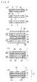
- Fig. 4 is a sectional view of the process for a conventional method of manufacturing double-side circuit boards for inner layers.
- the substrate is formed of prepreg sheet 21.
- the prepreg sheet 21 has a shape of 250 mm sq. and about 150 ⁇ m thick.
- the prepreg sheet 21 is formed of a composite material having non-woven cloth made from aromatic polyamide fiber and thermosetting epoxy resin impregnated to the non-woven fabric.
- Releasing films 22a, 22b have a plastic film and a Si type releasing agent applied to one side of the film, and the releasing films 22a, 22b are about 16 ⁇ m in thickness.
- plastic film polyethylene terephthalate is employed.
- Japanese Laid-open Patent No. 7-106760 refers to a method of continuously bonding releasing films 22a, 22b by dissolving the resin component of prepreg 21 with the use of a laminating apparatus.
- a through-hole 23 is formed in the pregreg sheet 21 and releasing films 22a, 22b bonded together.
- the through-hole 23 is filled with conductive paste 24.
- Metallic foils 25a, 25b such as copper of 18 ⁇ m thick are bonded to either side of the prepreg sheet 21.
- the conductive paste 24 is electrically connected to the metallic foil 25a, 25b.
- releasing films 22a, 22b are bonded to either side of the prepreg sheet 21.
- the through-holes 23 are formed, at predetermined portions, in the prepreg sheet 21 with the releasing films 22a, 22b bonded thereto, by using a laser beam machining process.
- the conductive paste 24 is filled into the through-holes 23.
- the prepreg sheet 21 having the through-holes 23 is placed on the table of a printer (not shown) and the conductive paste 24 is directly printed on the releasing film 22a.
- the releasing films 22a, 22b serve a function as a printing mask and also a function to prevent contamination of the prepreg sheet 21.
- the metallic foils 25a, 25b are laminated to either side of the prepreg sheet 21. And the laminated metallic foils 25a, 25b and prepreg sheet 21 are heated under pressures at a temperature of about 200°C and pressure of about 4MPa for one hour in a vacuum.
- the prepreg sheet 21 is compressed and becomes reduced in thickness (t2) to approximately 100 ⁇ m.
- the prepreg sheet 21 and metallic foils 25a, 25b are bonded to each other.
- the metallic foil 25a disposed on the surface side and the metallic foil 25b disposed on the back side are electrically connected to each other by the conductive paste 24 filled in the through-holes 23 formed at the predetermined positions.
- circuit patterns 31a, 31b are formed respectively on either side thereof.
- a double-side circuit board can be obtained.
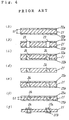
- Fig. 5 is a sectional view of the process for a conventional method of manufacturing a multi-layer circuit board, and the multi-layer circuit board is a four-layer circuit board.
- a double-side circuit board 40 having circuit patterns 31a, 31b manufactured by the steps from (a) to (g) of Fig. 4 and prepreg sheets 21a, 21b with conductive paste 24 filled in through-holes 23 manufactured by the steps from (a) to (d) of Fig. 4 are prepared.
- metallic foil 25b, prepreg sheet 21b, inner layer double-side circuit board 40, prepreg sheet 21a, and metallic foil 25a are positioned and laminated in this order.
- the laminated board formed of these is heated under pressures at a temperature of about 200°C and pressure of about 4MPa for one hour in a vacuum, thereby curing the prepreg sheets 21a, 21b.
- the prepreg sheets 21a, 21b are compressed and become reduced in thickness (t2) to 100 ⁇ m, then the double-side circuit board 40 and metallic foils 25a, 25b are bonded to each other.
- the circuit pattern 31a and circuit pattern 31b of the double-side circuit board 40 are connected to the metallic foils 25a, 25b by inner via-holes filled with conductive paste 24.
- the metallic foils 25a, 25b are selectively etched, thereby forming the circuit patterns 32a, 32b. In this way, a circuit board having four layers can be obtained.
- the double-side circuit boards used for inner layers become decreased in strength and rigidity with decrease in thickness of the circuit boards.
- circuit pattern 31a is formed on the surface of double-side circuit board 40 where circuit pattern 31b is not formed on the back side of same, and the conductive paste 24 of prepreg sheet 21a is compressed and electrically connected to circuit pattern 32 that is the outermost layer.
- the double-side circuit board 40 is deformed by the equivalent to the thickness of circuit pattern 31b on the back side of same and comes in contact with the prepreg sheet 21b.
- the conductive paste 24 of conductive paste 24B is less compressed as compared with the conductive paste 24 of conductive paste 24A.
- the connection resistance will become unstable.
- a multi-layer circuit board of the present invention comprises:
- a method of manufacturing a multi-layer circuit board of the present invention comprises:
- deformation of the inner layer circuit board can be prevented when a laminated substrate is laminated to one or either side of the inner layer circuit board by heating under pressures. Further, deformation of the prepreg sheet which forms the laminated substrate can be prevented. Accordingly, a plurality of through conductors for each of the inner layer circuit board and laminated substrate are formed in same length. As a result, the connection resistance between respective circuit patterns becomes stabilized.
- Fig. 1 is a sectional view of the process for a method of manufacturing an inner layer double-side circuit board in an embodiment of the present invention.
- Fig. 2 is a sectional view of the process for a method of manufacturing a multi-layer circuit board in an embodiment of the present invention.
- Fig. 3 is a sectional view of the process for a method of manufacturing a multi-layer circuit board in another embodiment of the present invention.
- Fig. 4 is a sectional view of the process for a method of manufacturing an inner layer double-side circuit board in a conventional example.
- Fig. 5 is a sectional view of the process for a method of manufacturing a multi-layer circuit board in a conventional example.
- Fig. 6 is a sectional view of a multi-layer circuit board for the description of the problems of the multi-layer circuit board in a conventional example.
- An inner layer circuit board with a convex inner layer circuit pattern having a predetermined thickness disposed on a substrate, a prepreg sheet with conductive material disposed in a plurality of through-holes, and a metallic foil are laminated to each other, and the laminated board is heated under pressures. After that, a laminated circuit pattern is formed by machining the metallic foil.
- a smoothing layer is disposed on a concave portion where the inner layer circuit pattern of the inner layer circuit board is not formed. In this way, the conductive materials filled in the plurality of through-holes are uniformly compressed when they are heated under pressures. As a result, the connection resistance between the inner layer circuit pattern and the laminated circuit pattern is stabilized.
- a multi-layer circuit board of the present invention comprises:
- the inner layer circuit board is a double-side circuit board with through conductors formed in the inner layer substrate;
- connection resistance between the circuit patterns disposed on either side of the double-side circuit board becomes stabilized. That is, the connection resistance between the first circuit pattern and the second circuit pattern is stabilized. Further, the connection resistance between the laminated circuit pattern and the inner layer circuit pattern is stabilized. That is, the connection resistance between the third circuit pattern and the first circuit pattern becomes stable. Further, the connection resistance between the fourth circuit pattern and the second circuit pattern is stabilized.
- the smoothing layer has a thickness equivalent to the predetermined thickness of the inner layer circuit pattern.
- the inner layer substrate is formed by heating and compressing a prepreg sheet having fiber aggregate and resin impregnated to the fiber aggregate.
- the smoothing layer contains resin, and the resin contained in the smoothing layer is same material as the resin contained in the inner layer substrate.
- the resin contains thermosetting resin.
- the laminated circuit pattern is electrically connected to the inner layer circuit pattern by the through conductors.
- the through conductor is made from conductive paste filled in through-holes formed in the laminated substrate.
- the laminated substrate includes a second through conductor penetrating the second substrate and a third through conductor penetrating the third substrate;
- the inner layer circuit board includes a plurality of inner layer circuit boards
- the inner layer circuit boards include a first inner layer circuit board and a second inner layer circuit board;
- At least one of the inner layer substrate and the laminated substrate is formed of a prepreg sheet feasible to be compressed under pressures.
- the fiber aggregate includes at least one of woven and non-woven cloth using aromatic polyamide as main material;
- small diameter through-holes can be easily formed by a laser beam machining process or the like, and multi-layer circuit boards having excellent physical strength and high circuit capacity can be realized.
- the fiber aggregate includes a fiber using at least one of glass fiber and ceramic fiber as a main material, and
- the laminated circuit pattern includes a plurality of through conductors electrically connected to the inner layer circuit pattern, and
- a method of manufacturing a multi-layer circuit board of the present invention comprises:
- the convex inner layer circuit pattern has a predetermined thickness, and a smoothing layer is formed on the substrate where the convex circuit pattern is not formed. Accordingly, the uniformity of heat and pressure application is enhanced, and the conductive paste is uniformly compressed. As a result, the connection resistance between the inner layer circuit pattern and the laminated circuit pattern becomes stabilized.
- the process of forming the smoothing layer includes:
- the process of forming the smoothing layer includes:
- the inner layer circuit board is improved in strength and rigidity. Accordingly, positioning becomes easier in lamination of multiple layers, and further, there is no generation of resin running and it is possible to prevent deflection of respective circuit pattern positions.
- the smoothing layer is formed in a manner such that the smoothing layer is same in height as the thickness of the inner layer circuit pattern.
- the process of forming the inner layer circuit board includes:
- connection resistance between the inner layer circuit pattern and laminated circuit pattern disposed on either side of the inner substrate may be stabilized.
- the process of preparing the prepreg sheet includes:
- the process of laminating the prepreg sheet and the metallic foil to the surface of the smoothing layer and the inner layer circuit pattern disposed on the inner layer circuit board includes:
- the inner layer substrate and the prepreg sheet are feasible to be compressed.
- the prepreg sheet includes fiber aggregate and resin impregnated to the fiber aggregate, and the prepreg sheet is feasible to be compressed, and
- the fiber aggregate includes at least one of non-woven cloth and woven cloth.
- the fiber aggregate is made from at least one selected from the group consisting of aromatic polyamide, glass and ceramic.
- the smoothing layer contains resin.
- the prepreg sheet includes a plurality of through-holes and conductive material disposed in the plurality of through-holes;
- the prepreg sheet is feasible to be compressed, and the prepreg sheet includes a plurality of through-holes and conductive material disposed in the plurality of through-holes;
- a multi-layer circuit board in an exemplary embodiment of the present invention and a method of manufacturing same will be described in the following with reference to Figs. 1 to 3.
- Fig. 1 is a sectional view showing the process for a method of manufacturing a multi-layer circuit board in an exemplary embodiment of the present invention. Particularly, it shows the process for manufacturing a double-side circuit board as an inner layer circuit board used for a multi-layer circuit board.
- Fig. 2 is a sectional view of the process for a method of manufacturing a multi-layer circuit board in an exemplary embodiment of the present invention.
- the multi-layer circuit board shown in Fig. 2 includes a four-layer circuit pattern.
- inner layer prepreg sheet 1 (first prepreg sheet) is manufactured as an inner substrate.
- the inner layer prepreg sheet 1 is 250 mm square and about 130 ⁇ m in thickness (t1).
- the inner layer prepreg 1 includes a composite material containing non-woven cloth as fiber aggregate and resin impregnated to the non-woven cloth.
- aromatic polyamide fiber is employed.
- thermosetting epoxy resin is employed.
- Each of a first releasing film 2a and a second releasing film 2b includes a Si type releasing agent applied to one side thereof.
- the releasing films 2a, 2b are approximately 16 ⁇ m in thickness.
- polyethylene terephthalate is employed as the releasing films 2a, 2b.
- the first releasing film 2a is bonded to one side of the inner layer prepreg sheet 1, and the second releasing film 2b is bonded to the other side of the inner layer prepreg sheet 1. Then, the first releasing film 2a, the second releasing film 2b, and the inner layer prepreg sheet 1 are bonded together by means of a laminating apparatus. In the laminating process using a laminating apparatus, the resin component contained in the inner prepreg sheet 1 is melted, and the molten resin serves a function as adhesive.
- through-holes 3 are formed in the predetermined portion of the inner layer prepreg sheet 1 with the first releasing film 2a and the second releasing film 2b bonded thereto by using a laser beam machining process.
- conductive paste 4 as a conductive material is filled into the through-holes 3.
- the conductive paste 4 filled in the through-holes 3 forms through conductors.
- the conductive paste 4 is made from resin component and conductive powder dispersed in the resin component.
- the conductive powder for example, copper powder of 2 ⁇ m in average grain diameter is used.
- the resin for example, solventless thermosetting epoxy resin and acid-anhydride hardening agent are used. A mixture of 85% by weight of conductive powder, 12.5% by weight of thermosetting epoxy resin, and 2.5% by weight of hardening agent is sufficiently kneaded by three rolls to manufacture the conductive paste 4.
- the method of filling the conductive paste 4 into the through-holes 3 comprises a step of placing the laminated board of releasing films 2a, 2b and inner layer prepreg sheet 1 having through-holes 3 on the table of a printer (not shown), and a step of directly filling the conductive paste 4 into the through-holes 3 from above the releasing film 2a. Then, the first releasing film 2a and the second releasing film 2b serve a function as a printing mask and also a function to prevent contamination of the inner layer prepreg sheet 1.
- first metallic foil 5a is laminated to one side of inner layer prepreg sheet 1 having conductive paste filled in through-holes
- second metallic foil 5b is laminated to the other side of the inner layer prepreg sheet 1.
- the first metallic foil 5a and the second metallic foil 5b are 300 mm square and 18 ⁇ m in thickness.
- the laminated first metallic foil 5a, inner prepreg sheet 1 and second metallic foil 5b are heated under pressures at a temperature of about 200°C and pressure of about 4MPa for one hour in a vacuum or inactive gas.
- the inner layer prepreg sheet 1 is compressed to about 90 ⁇ m in thickness, and also, the inner layer prepreg sheet 1, first metallic foil 5a and second metallic foil 5b are bonded together. Due to the process of heating under pressures, epoxy resin chemically reacts with the curing agent and is cured, and thereby, the inner layer prepreg sheet 1 changes and forms an inner layer substrate 1a.
- the conductive paste 4 filled in the through-holes forms inner layer through conductors 4a.
- the first metallic foil 5a and the second metallic foil 5b are electrically connected to each other by the inner layer through conductors 4a.
- the first metallic foil 5a is selectively etched, and then a first circuit pattern 6a as an inner layer circuit pattern is formed.
- the second metallic foil 5b is selectively etched, and a second circuit pattern 6b as an inner layer circuit pattern is formed.
- These circuit patterns 6a, 6b are convex in shape.
- a first concave portion 6g and a second concave portion 6h subjected to etching are concave in shape.
- a first smoothing layer 7a is disposed on the first concave portion 6g where the circuit patterns 6a, 6b are not formed.
- a second smoothing layer 7b is disposed on-the second concave portion 6h.
- the surfaces of the first circuit pattern 6a and the first smoothing layer 7a are same in height.
- the surfaces of the second circuit pattern 6b and the second smoothing layer 7b are also same in height.
- a smoothing layer 7 is formed on the inner layer substrate 1a. In this way, a double-side circuit board 20 can be obtained as an inner layer circuit board.
- the method of forming the smoothing layer 7 comprises a step of coating the first concave portion 6c and the second concave portion 6d with a material which contains resin, by using a squeezing method or the like.
- a material which contains a solvent and resin dissolved in the solvent is evaporated by heating.
- the type of the resin used is not limited, and for example, thermosetting epoxy resin is used.
- the solvent for example, methyl ethyl ketone or the like is used.
- stage B stands for a state of being semi-hard.
- the smoothing layer 7 is not limited to the smoothing layer 7 in a state of stage B mentioned above, but it is possible to use a smoothing layer described in the following. That is, another method of forming the smoothing layer 7 comprises a step of coating the concave portions 6c, 6d with thermosetting resin component thicker than the circuit patterns 6a, 6b, and a step of forming a thermosetting resin layer by heating the coated thermosetting resin component, and a step of exposing the circuit patterns 6a, 6b by polishing the thermosetting resin layer. The smoothing layer 7 is formed by this method.
- thermosetting resin component coated with the thermosetting resin component.
- the thermosetting resin component coated on the circuit patterns 6a, 6b is removed by polishing or the like.
- epoxy resin is used as the thermosetting resin component.
- the thickness of the smoothing layer 7 formed on either side of double-side circuit board is nearly equal to the thickness of circuit patterns 7a, 7b.
- Fig. 2 is a sectional view of the process for a method of manufacturing a multi-layer circuit board in an embodiment of the present invention.
- a multi-layer circuit board shown in Fig. 2 is an example of a four-layer circuit board having four-layers of circuit patterns.
- a double-side circuit board 20 manufactured by the method of Fig. 1 is prepared.
- the double-side circuit board 20 has smoothing layers 7 formed on concave portions except convex inner layer circuit patterns 6a, 6b.
- the first circuit pattern 6a as an inner layer circuit pattern is electrically connected to the second circuit pattern 6b by inner layer through conductors 4a disposed in through-holes.
- two prepreg sheets 10a, 10b having conductive paste 4 are formed as in the processes (a) through (d) in Fig. 1.
- the second prepreg sheet 10a has conductive paste 4 filled in through-holes
- the third prepreg sheet 10b also has conductive paste 4 filled in through holes.
- third metallic foil 8a and fourth metallic foil 8b are prepared. These metallic foils 8a, 8b are formed of copper and 300 mm square having a thickness of 18 ⁇ m.
- the fourth metallic foil 8b, third prepreg sheet 10b having conductive paste, double-side circuit board 20, second prepreg sheet 10a having conductive paste, and third metallic foil 8a are positioned and laminated in this order.
- the laminated material is heated under pressures at a temperature of about 200°C and pressure of about 4MPa for one hour in a vacuum or inactive gas.
- the two prepreg sheets 10a, 10b are compressed to about 90 ⁇ m in thickness (t2), and also, the resin component contained in the prepreg sheets 10a, 10b are cured.
- the second prepreg sheet 10a forms a second substrate 1b
- the third prepreg sheet 10b forms a third substrate 1c.
- the conductive paste 4 filled in the through-holes of prepreg sheets 10a, 10b form through conductors 4b.
- the double-side circuit board 20 and respective metallic foils 8a, 8b are bonded to each other. Furthermore, the first circuit pattern 6a makes inner via-hole connection to the third metallic foil 8a by through conductors 4b, and the second circuit pattern 6b makes inner via-hole connection to the fourth metallic foil 8b by through conductors 4b.
- the third metallic foil 8 and fourth metallic foil 8b are selectively etched, and thereby, third circuit pattern 9a and fourth circuit pattern 9b are formed as laminated circuit patterns.
- a six-layer circuit board can be obtained by using the above four-layer circuit board instead of the double-side circuit board 20.
- a three-layer circuit board having a three-layer circuit patterns can be obtained by using only the second prepreg sheet 10a without using the third prepreg sheet 10b.
- a six-layer circuit board having six-layer circuit patterns can be obtained by using the above four-layer circuit board instead of the double-side circuit board 20.
- smoothing layers 7a, 7b are disposed on concave portions 6g, 6h of circuit patterns 6a, 6b, all portions of the double-side circuit board 20 become uniform in thickness and smoothness. Accordingly, the pressure will be uniformly applied so that the through conductors 4a disposed in respective through-holes become same in length without causing change in thickness of the first substrate 1a and of the first circuit pattern 6a and the second circuit pattern 6b. As a result, the connection resistance between the circuit patterns is stabilized.
- Fig. 3 is a sectional view of the process for a method of manufacturing a multi-layer circuit board in the second exemplary embodiment.
- the multi-layer circuit board of Fig. 3 has six layers of circuit patterns.
- a second double-side circuit board 20a and third double-side circuit board 20b are used, which have the same configuration as the double-side circuit board 20 manufactured by the steps (a) through (h) shown in Fig. 1 of the first exemplary embodiment described above.
- the second double-side circuit board 20a includes a first circuit pattern 6a and second circuit pattern 6b disposed on either side of a substrate.
- the second double-side circuit board 20b includes a fifth circuit pattern 6c and sixth circuit pattern 6d disposed on either side of a substrate. Smoothing layer 7 is formed on the concave portions of respective circuit patterns 6a, 6b, 6c, 6d.
- the respective double-side circuit boards 20a, 20b have through conductors 4a disposed in through-holes.
- the first circuit pattern 6a and the second circuit pattern 6b are electrically connected to each other by the through conductors 4a.
- the fifth circuit pattern 6c and the sixth circuit pattern 6d are electrically connected to each other by the through conductors 4a.
- Three prepreg sheets are formed, which have the same configuration as the prepreg sheet 10 with through conductors manufactured by the steps (a) through (d) shown in Fig. 1 of the first exemplary embodiment described above. That is, a second prepreg sheet 10a having conductive material 4 disposed in through-holes, a third prepreg sheet 10b having conductive material 4 disposed in through-holes, and a fourth prepreg sheet 10c having conductive material 4 disposed in through-holes are formed in the same way as in the first exemplary embodiment.
- the conductive material conductive paste is used as the conductive material.
- third copper foil 8a and fourth copper foil 8b are prepared as the metallic foils to be used.
- the metallic foils 8a, 8b are 300 mm square and 18 ⁇ m in thickness.
- the fourth metallic foil 8b, fourth prepreg sheet 10c, second double-side circuit board 20b, third prepreg sheet 10b, first double-side circuit board 20a, second prepreg sheet 10a, and third metallic foil 8a are positioned and laminated in this order.
- the laminated board is heated under pressures at a temperature of about 200°C and pressure of about 4MPa for one hour in a vacuum or inactive gas.
- the resin components of respective prepreg sheets 10a, 10b, and 10c are cured, and simultaneously, the prepreg sheets 10a, 10b, 10c are compressed to about 90 ⁇ m in thickness (t2).
- the prepreg sheets 10a, 10b, 10c, the double-side circuit boards 20a, 20b, and the metallic foils 8a, 8b are respectively bonded to each other.
- the prepreg sheets 10a, 10b, 10c respectively form substrates 1b, 1c, 1d.
- the conductive paste 4 filled in the through-holes forms through conductors 4b.
- the circuit patterns 6a, 6b, 6c, 6d respectively establish inner via-hole connections to the metallic foils 8a, 8b by through conductors 4b.
- the third metallic foil 8 is selectively etched, and thereby, third circuit pattern 9a is formed as a laminated circuit pattern. Also, the fourth metallic foil 8b is selectively etched, and fourth circuit pattern 9b is formed as a laminated circuit pattern. In this way, a multi-layer circuit board having six layers of circuit patterns can be obtained.
- double-side circuit board 20 In place of the method of manufacturing double-side circuit board 20 in the first exemplary embodiment, it is possible to employ a method of manufacturing a double-side circuit board as described in the following.
- step (b) of Fig. 1 through-holes 3 are formed by drilling. Also, through conductors precipitated by metal-plating are disposed instead of conductive paste.
- the other steps are same as in the first exemplary embodiment. That is, smoothing layers 7a, 7b are formed on the concave portions 6g, 6h of respective circuit patterns of the double-side circuit boards used as inner layers.
- heat resisting materials such as heat resistant polymer, glass, ceramic and inorganic material are used as fiber aggregate used for prepreg sheets.
- a prepreg sheet it is also possible to use a composite material comprising non-woven glass fiber cloth and thermosetting epoxy resin impregnated in the non-woven glass fiber cloth.
- thermosetting epoxy resin instead of aromatic polyamide fiber, ceramic fiber can be used.
- non-woven cloth woven cloth can be used.
- thermosetting epoxy resin other types of thermosetting resin can be used.
- high temperature resisting resin such as polyamide can be used.
- the inner layer circuit patterns include a first circuit pattern 1a and second circuit pattern 1b disposed on either side of substrate 1a.
- the configuration is not limited to this, but the following configuration is also usable. That is, only a first circuit pattern as an inner layer circuit pattern is disposed on one side of a substrate, and no inner layer circuit pattern is disposed on the other side of the substrate. And, a smoothing layer is disposed on the concave portion of the first circuit pattern.
- the number of steps required for forming a multi-layer circuit board is fewer than required in the case of a configuration with an inner circuit pattern disposed on one side of a substrate.
- a smoothing layer is formed on the convex portion of the circuit pattern of an inner layer circuit board. Accordingly, in the process of manufacturing a multi-layer circuit board, deformation of the inner layer circuit board can be prevented when a laminated substrate is heated under pressures while being laminated to one or either side of the inner layer circuit board. Further, deformation of the laminated substrate can be prevented. Therefore, a plurality of through conductors disposed in respective through-holes of the inner layer circuit boards and laminated substrates are uniformly pressurized. As a result, the connection reaction between the respective circuit patterns becomes stable.
- the inner layer circuit board is a double-side circuit board
- disposing smoothing layers on the convex portions of circuit patterns causes the double-side circuit board to become uniform in thickness and smoothness at all portions thereof.
- the through conductors disposed in respective through-holes are uniformly pressurized without changing the thickness of the first substrate, the first circuit pattern and the second circuit pattern.
- the connection resistance between the first circuit pattern and the second circuit pattern becomes stabilized, and thereby, a multi-layer circuit board that ensures stable connection resistance may be obtained.
Landscapes
- Engineering & Computer Science (AREA)
- Manufacturing & Machinery (AREA)
- Microelectronics & Electronic Packaging (AREA)
- Production Of Multi-Layered Print Wiring Board (AREA)
- Printing Elements For Providing Electric Connections Between Printed Circuits (AREA)
- Reinforced Plastic Materials (AREA)
Applications Claiming Priority (2)
| Application Number | Priority Date | Filing Date | Title |
|---|---|---|---|
| JP2000247331 | 2000-08-17 | ||
| JP2000247331A JP3903701B2 (ja) | 2000-08-17 | 2000-08-17 | 多層回路基板とその製造方法 |
Publications (2)
| Publication Number | Publication Date |
|---|---|
| EP1180921A2 true EP1180921A2 (de) | 2002-02-20 |
| EP1180921A3 EP1180921A3 (de) | 2005-12-07 |
Family
ID=18737446
Family Applications (1)
| Application Number | Title | Priority Date | Filing Date |
|---|---|---|---|
| EP01117144A Withdrawn EP1180921A3 (de) | 2000-08-17 | 2001-07-13 | Mehrschichtige Leiterplatte und Verfahren zu deren Herstellung |
Country Status (5)
| Country | Link |
|---|---|
| US (1) | US6528733B2 (de) |
| EP (1) | EP1180921A3 (de) |
| JP (1) | JP3903701B2 (de) |
| CN (1) | CN100469215C (de) |
| TW (1) | TW511441B (de) |
Cited By (2)
| Publication number | Priority date | Publication date | Assignee | Title |
|---|---|---|---|---|
| US6694612B1 (en) * | 1999-05-18 | 2004-02-24 | Matsushita Electric Industrial Co., Ltd. | Mask film having a non-parting portion |
| CN113660768A (zh) * | 2021-08-13 | 2021-11-16 | 东风汽车集团股份有限公司 | 一种防破解多层pcb及其制作方法 |
Families Citing this family (18)
| Publication number | Priority date | Publication date | Assignee | Title |
|---|---|---|---|---|
| JP2002064270A (ja) * | 2000-08-17 | 2002-02-28 | Matsushita Electric Ind Co Ltd | 回路基板とその製造方法 |
| US20050146025A1 (en) * | 2001-02-26 | 2005-07-07 | John Gregory | Method of forming an opening or cavity in a substrate for receiving an electronic component |
| US6855892B2 (en) * | 2001-09-27 | 2005-02-15 | Matsushita Electric Industrial Co., Ltd. | Insulation sheet, multi-layer wiring substrate and production processes thereof |
| JP3801158B2 (ja) * | 2002-11-19 | 2006-07-26 | セイコーエプソン株式会社 | 多層配線基板の製造方法、多層配線基板、電子デバイス及び電子機器 |
| US7181839B2 (en) * | 2003-01-14 | 2007-02-27 | Matsushita Electric Industrial Co., Ltd. | Method for producing a circuit board |
| US7013452B2 (en) * | 2003-03-24 | 2006-03-14 | Lucent Technologies Inc. | Method and apparatus for intra-layer transitions and connector launch in multilayer circuit boards |
| JP4131694B2 (ja) * | 2003-10-06 | 2008-08-13 | 三洋電機株式会社 | 積層セラミックス基板及びその製造方法 |
| US20050121225A1 (en) * | 2003-12-03 | 2005-06-09 | Phoenix Precision Technology Corporation | Multi-layer circuit board and method for fabricating the same |
| US20050124197A1 (en) * | 2003-12-04 | 2005-06-09 | Matsushita Electric Industrial Co., Ltd. | Circuit board and method for manufacturing the same, semiconductor package, component built-in module and board for electronic equipment |
| FI121134B (fi) * | 2005-06-16 | 2010-07-15 | Imbera Electronics Oy | Menetelmä piirilevyrakenteen valmistamiseksi ja piirilevyrakenne |
| JP2007263862A (ja) * | 2006-03-29 | 2007-10-11 | Kyocera Corp | プローブカード用基板、半導体検査装置、およびその製造方法 |
| KR101031010B1 (ko) * | 2008-10-29 | 2011-04-25 | 삼성메디슨 주식회사 | 피씨비 및 이를 구비하는 프로브 |
| TWI402173B (zh) * | 2008-11-17 | 2013-07-21 | Fujitsu Ltd | 電路板及其製造方法(一) |
| US8383948B2 (en) * | 2009-09-18 | 2013-02-26 | Ibiden Co., Ltd. | Flex-rigid wiring board and method for manufacturing the same |
| DE102010041121A1 (de) * | 2010-09-21 | 2012-03-22 | Robert Bosch Gmbh | Schaltungsträger sowie Verfahren zur Herstellung eines Schaltungsträgers |
| JP2016219452A (ja) * | 2015-05-14 | 2016-12-22 | 富士通株式会社 | 多層基板及び多層基板の製造方法 |
| US10801137B2 (en) | 2016-07-21 | 2020-10-13 | International Business Machines Corporation | Glass cloth including attached fibers |
| TWI752820B (zh) * | 2021-02-08 | 2022-01-11 | 欣興電子股份有限公司 | 電路板結構及其製作方法 |
Family Cites Families (9)
| Publication number | Priority date | Publication date | Assignee | Title |
|---|---|---|---|---|
| DE3113334A1 (de) * | 1981-04-02 | 1982-10-28 | Siemens AG, 1000 Berlin und 8000 München | Verfahren zur herstellung von mehrlagenleiterplatten |
| FR2666190B1 (fr) * | 1990-08-24 | 1996-07-12 | Thomson Csf | Procede et dispositif d'encapsulation hermetique de composants electroniques. |
| JP2601128B2 (ja) | 1992-05-06 | 1997-04-16 | 松下電器産業株式会社 | 回路形成用基板の製造方法および回路形成用基板 |
| US5779870A (en) * | 1993-03-05 | 1998-07-14 | Polyclad Laminates, Inc. | Method of manufacturing laminates and printed circuit boards |
| CN1044762C (zh) * | 1993-09-22 | 1999-08-18 | 松下电器产业株式会社 | 印刷电路板及其制造方法 |
| JPH08302161A (ja) * | 1995-05-10 | 1996-11-19 | Hitachi Chem Co Ltd | 樹脂組成物及びその樹脂組成物をケミカルエッチングする方法 |
| JP3230727B2 (ja) * | 1996-08-08 | 2001-11-19 | 松下電器産業株式会社 | 多層プリント配線板及びその製造方法 |
| US5837355A (en) * | 1996-11-07 | 1998-11-17 | Sumitomo Bakelite Company Limited | Multilayer printed circuit board and process for producing and using the same |
| EP1895586A3 (de) * | 1997-10-17 | 2013-04-03 | Ibiden Co., Ltd. | Substrat für eine Halbleiterpackung |
-
2000
- 2000-08-17 JP JP2000247331A patent/JP3903701B2/ja not_active Expired - Fee Related
-
2001
- 2001-06-01 TW TW090113377A patent/TW511441B/zh not_active IP Right Cessation
- 2001-06-27 CN CNB011225211A patent/CN100469215C/zh not_active Expired - Fee Related
- 2001-07-12 US US09/902,800 patent/US6528733B2/en not_active Expired - Fee Related
- 2001-07-13 EP EP01117144A patent/EP1180921A3/de not_active Withdrawn
Cited By (4)
| Publication number | Priority date | Publication date | Assignee | Title |
|---|---|---|---|---|
| US6694612B1 (en) * | 1999-05-18 | 2004-02-24 | Matsushita Electric Industrial Co., Ltd. | Mask film having a non-parting portion |
| US7066344B2 (en) | 1999-05-18 | 2006-06-27 | Matsushita Electric Industrial Co., Ltd. | Mask film, its manufacturing method, and manufacturing method of circuit board using the same |
| CN113660768A (zh) * | 2021-08-13 | 2021-11-16 | 东风汽车集团股份有限公司 | 一种防破解多层pcb及其制作方法 |
| CN113660768B (zh) * | 2021-08-13 | 2023-02-28 | 东风汽车集团股份有限公司 | 一种防破解多层pcb及其制作方法 |
Also Published As
| Publication number | Publication date |
|---|---|
| TW511441B (en) | 2002-11-21 |
| JP2002064269A (ja) | 2002-02-28 |
| US6528733B2 (en) | 2003-03-04 |
| CN1339940A (zh) | 2002-03-13 |
| US20020020548A1 (en) | 2002-02-21 |
| EP1180921A3 (de) | 2005-12-07 |
| CN100469215C (zh) | 2009-03-11 |
| JP3903701B2 (ja) | 2007-04-11 |
Similar Documents
| Publication | Publication Date | Title |
|---|---|---|
| US6528733B2 (en) | Multi-layer circuit board and method of manufacturing same | |
| EP1180920B1 (de) | Verfahren zur Herstellung einer Leiterplatte | |
| US6664127B2 (en) | Method of manufacturing multi-layer printed wiring board | |
| JP3197213B2 (ja) | プリント配線板およびその製造方法 | |
| JP2587596B2 (ja) | 回路基板接続材とそれを用いた多層回路基板の製造方法 | |
| US20020053465A1 (en) | Circuit board electrically insulating material, circuit board and method for manufacturing the same | |
| WO2001045478A1 (en) | Multilayered printed wiring board and production method therefor | |
| KR101116079B1 (ko) | 다층 프린트 배선판의 제조방법 및 다층 프린트 배선판 | |
| KR20010105375A (ko) | 다중-층 인쇄 회로를 위한 적층 | |
| JP3207663B2 (ja) | プリント配線基板及びその製造方法 | |
| CN101257773B (zh) | 多层印刷电路板的制造方法 | |
| KR100755795B1 (ko) | 다층 회로 기판의 제조 방법 | |
| JP3738536B2 (ja) | プリント配線基板の製造方法 | |
| JPH08316598A (ja) | プリント配線板およびその製造方法 | |
| JP5077800B2 (ja) | 多層プリント配線板の製造方法 | |
| JP3588888B2 (ja) | 多層プリント配線基板の製造方法 | |
| JP2006313932A (ja) | 多層回路基板とその製造方法 | |
| KR101281898B1 (ko) | 다층 프린트배선판 및 그 제조방법 | |
| WO2017046762A1 (en) | Sacrificial structure comprising low-flow material for manufacturing component carriers | |
| JP3238901B2 (ja) | 多層プリント配線基板およびその製造方法 | |
| JP2002103494A (ja) | プリプレグとプリント配線基板およびその製造方法 | |
| JPH11274720A (ja) | 多層積層板の製造方法 | |
| KR20040065861A (ko) | 전층 ivh공법의 인쇄회로기판 및 이의 제조방법 | |
| JP4622939B2 (ja) | 回路基板の製造方法 | |
| JP5077801B2 (ja) | 多層プリント配線板の製造方法 |
Legal Events
| Date | Code | Title | Description |
|---|---|---|---|
| PUAI | Public reference made under article 153(3) epc to a published international application that has entered the european phase |
Free format text: ORIGINAL CODE: 0009012 |
|
| AK | Designated contracting states |
Kind code of ref document: A2 Designated state(s): AT BE CH CY DE DK ES FI FR GB GR IE IT LI LU MC NL PT SE TR |
|
| AX | Request for extension of the european patent |
Free format text: AL;LT;LV;MK;RO;SI |
|
| PUAL | Search report despatched |
Free format text: ORIGINAL CODE: 0009013 |
|
| AK | Designated contracting states |
Kind code of ref document: A3 Designated state(s): AT BE CH CY DE DK ES FI FR GB GR IE IT LI LU MC NL PT SE TR |
|
| AX | Request for extension of the european patent |
Extension state: AL LT LV MK RO SI |
|
| 17P | Request for examination filed |
Effective date: 20060127 |
|
| AKX | Designation fees paid |
Designated state(s): DE FR GB |
|
| RAP1 | Party data changed (applicant data changed or rights of an application transferred) |
Owner name: PANASONIC CORPORATION |
|
| 17Q | First examination report despatched |
Effective date: 20090730 |
|
| STAA | Information on the status of an ep patent application or granted ep patent |
Free format text: STATUS: THE APPLICATION HAS BEEN WITHDRAWN |
|
| 18W | Application withdrawn |
Effective date: 20111024 |