EP1182802B1 - Dreifaches Datenpuffersystem für Kommunikationsanordnungen mit Hochdatenraten - Google Patents
Dreifaches Datenpuffersystem für Kommunikationsanordnungen mit Hochdatenraten Download PDFInfo
- Publication number
- EP1182802B1 EP1182802B1 EP01000399.4A EP01000399A EP1182802B1 EP 1182802 B1 EP1182802 B1 EP 1182802B1 EP 01000399 A EP01000399 A EP 01000399A EP 1182802 B1 EP1182802 B1 EP 1182802B1
- Authority
- EP
- European Patent Office
- Prior art keywords
- data
- slot
- aligned
- multiplexer
- data buffer
- Prior art date
- Legal status (The legal status is an assumption and is not a legal conclusion. Google has not performed a legal analysis and makes no representation as to the accuracy of the status listed.)
- Expired - Lifetime
Links
- 230000006854 communication Effects 0.000 title claims description 19
- 238000004891 communication Methods 0.000 title claims description 18
- 239000007853 buffer solution Substances 0.000 title description 6
- 239000000872 buffer Substances 0.000 claims description 79
- 230000010365 information processing Effects 0.000 claims description 6
- 230000004044 response Effects 0.000 claims description 4
- 238000012545 processing Methods 0.000 description 17
- 238000010586 diagram Methods 0.000 description 10
- 241001442055 Vipera berus Species 0.000 description 7
- 238000000034 method Methods 0.000 description 7
- 230000035508 accumulation Effects 0.000 description 3
- 238000009825 accumulation Methods 0.000 description 3
- 230000008859 change Effects 0.000 description 3
- 230000001427 coherent effect Effects 0.000 description 3
- 230000006870 function Effects 0.000 description 3
- 238000012986 modification Methods 0.000 description 2
- 230000004048 modification Effects 0.000 description 2
- 238000012360 testing method Methods 0.000 description 2
- 230000004075 alteration Effects 0.000 description 1
- 230000005540 biological transmission Effects 0.000 description 1
- 238000010276 construction Methods 0.000 description 1
- 238000005314 correlation function Methods 0.000 description 1
- 238000013461 design Methods 0.000 description 1
- 238000001514 detection method Methods 0.000 description 1
- 238000009432 framing Methods 0.000 description 1
- 230000008569 process Effects 0.000 description 1
- 238000009877 rendering Methods 0.000 description 1
- 239000000243 solution Substances 0.000 description 1
- 238000001228 spectrum Methods 0.000 description 1
- 238000006467 substitution reaction Methods 0.000 description 1
Images

Classifications
-
- H—ELECTRICITY
- H04—ELECTRIC COMMUNICATION TECHNIQUE
- H04B—TRANSMISSION
- H04B7/00—Radio transmission systems, i.e. using radiation field
- H04B7/24—Radio transmission systems, i.e. using radiation field for communication between two or more posts
- H04B7/26—Radio transmission systems, i.e. using radiation field for communication between two or more posts at least one of which is mobile
- H04B7/2628—Radio transmission systems, i.e. using radiation field for communication between two or more posts at least one of which is mobile using code-division multiple access [CDMA] or spread spectrum multiple access [SSMA]
-
- H—ELECTRICITY
- H04—ELECTRIC COMMUNICATION TECHNIQUE
- H04B—TRANSMISSION
- H04B1/00—Details of transmission systems, not covered by a single one of groups H04B3/00 - H04B13/00; Details of transmission systems not characterised by the medium used for transmission
- H04B1/69—Spread spectrum techniques
- H04B1/707—Spread spectrum techniques using direct sequence modulation
- H04B1/7097—Interference-related aspects
- H04B1/711—Interference-related aspects the interference being multi-path interference
- H04B1/7115—Constructive combining of multi-path signals, i.e. RAKE receivers
Definitions
- This invention relates generally to data communication systems and methods, and more particularly to a minimally sized data buffer that allows vector processing of simultaneous frames of overlaying data in which the frames do not have the same starting position.
- the generic format of a frame consists of a preamble at the beginning of each burst.
- Some communication protocols additionally include data and end-of-frame.
- the preamble is used to signify (recognize) the start of transmission.
- All nodes on a network traditionally use the same preamble and the same end-of-frame. Each node, therefore, is required to decode at least the beginning of the data to identify if this message is addressed to itself. Decoding efforts importantly require a real-time computational complexity. Further, traditional data communication processes are made even more complex and time consuming due to the necessity to utilize collision detection and resolve techniques.
- CDMA code division multiple access
- European Patent Application No. 1128565 describes a programmable, flexible, vector correlation engine for CDMA mobile and base station chip rate signal processing.
- a correlator co-processor (CCP) performs the de-spreading tasks for a RAKE receiver, early/late correlations for time tracking, and has provision for coherent accumulation of different lengths.
- the CCP also performs energy estimation and non-coherent accumulation functions.
- the CCP can also perform correlation functions required for delay profile estimation, and for search/acquisition functions.
- the same centralized Data Path is used to perform all these functions; a common controller generates signals into the Data Path in response to tasks initiated by a host processor. The tasks written into the CCP are performed effectively in parallel by the CCP Data Path.
- United States Patent No. 5867527 describes an integrated search processor used in a modem for a spread spectrum communications system buffers receive samples and utilizes a time sliced transform processor operating on successive offsets from the buffer.
- the search processor autonomously steps through a search as configured by a microprocessor specified search parameter set, which can include the group of antennas to search over, the starting offset and width of the search window to search over, and the number of Walsh symbols to accumulate results at each offset.
- the search processor calculates the correlation energy at each offset, and presents a summary report of the best paths found in the search to use for demodulation element reassignment.
- the search is done in a linear fashion independent of the probability that a signal being searched for was transmitted at any given time.
- the present invention is directed to a triple data buffer for supporting high bit rate data communication systems such as the correlator co-processor (CCP) disclosed in European Patent Application No. 1128565 described above.
- CCP correlator co-processor
- the invention resides in a slot-aligned IQ data buffer (100) for high bit rate communication systems as set out in the appended claims.
- the CCP is capable of receiving multiple in-phase (I) and quadrature (Q) signal samples from multiple sources to accommodate antenna diversity wherein I and Q samples may be 6-bits or more.
- the I and Q samples further represent multiple overlaying channels, each of which have several multi-path elements, the aggregate data rate being possibly greater than the chip rate.
- the triple data buffer is a slot-aligned IQ buffer comprising three 16-chip buffers which are filled circularly.
- each of the 16-chip buffers contains 64 (4x oversampled) samples of 12-bits (6 for I and 6 for Q). When one of these 16-chip buffers is being processed, the one that holds the next 16 chips is used to access extra chips which are not in the current buffer.
- the alignment of the task's frame determines the starting chip to be processed and then the next 15 chips are required to do the correlator vector processing which is 16 chips wide. At most, 15 more chips might be required from the next buffer.
- Frame alignment is accomplished using three leve'ls of multiplexing.
- the first level selects a pair of buffers to be processed.
- the second level selects the sample number (0, 1, 2, 3 of the 4x oversamples) required.
- the third level selects the correct chips for the alignment of the slot and is implemented using a barrel shifter to provide a smaller configuration than necessary when using brute-force multiplexing techniques.
- an IQ data buffer is implemented to accommodate selection of IQ data bits which align to the frame/slot timing of each task.
- an IQ data buffer is implemented to more easily accommodate compressed mode and change of service requirements when receiving data.
- an IQ data buffer is implemented that provides a simple control logic capable of rendering improved testing features over known architectures.
- Still another aspect of the invention is associated with an IQ data buffer that maximizes power efficiency when executing correlations.
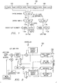
- FIG. 1 is a block diagram illustrating a slot-aligned IQ buffer 100 according to one embodiment of the present invention.
- the slot-aligned IQ buffer 100 is a triple data buffer system that allows vector processing of simultaneous frames of overlaying data in which the frames do not have the same starting position.
- a first data buffer 102, second data buffer 104 and third data buffer 106 allow the processing engine, such as a DSP associated with the CCP discussed herein above, to slide the selection of the vector to be processed so that it aligns with the framing of the data.
- CDMA and WCDMA communications employ overlaying coded data streams, each having its own frame timing.
- the slot-aligned IQ buffer 100 is particularly advantageous for CDMA and WCDMA systems because it allows for vastly simplified processing hardware.
- a WCDMA vector chip processor would require significant additional hardware just to support the compressed mode of operation in WCDMA.
- the slot-aligned IQ buffer 100 therefore allows for changing the way data is processed cleanly at boundaries in the data without requiring additional hardware to accommodate such changes.
- the slot-aligned IQ buffer 100 can be seen to include three 16-chip buffers 102, 104, 106.
- the buffers 102, 104, 106 are filled circularly; and each buffer 102, 104, 106 contains 64 (4x oversampled) samples of 12-bits (6 for I and 6 for Q).
- the one which holds the next 16 chips is used to access the extra chips which are not in the current buffer.
- the alignment of the task's frame determines the starting chip to be processed.
- the next 15 chips are then required to implement the correlator vector processing which is 16 chips wide. At most, 15 more chips might be required from the next buffer.
- There are three buffers 102, 104, 106 such that when the data in one buffer is processed, the next buffer can be used to access extra chips for processing while the third can be filled with incoming data.
- the first level of multiplexing 108 selects two of the three buffers 102, 104, 106, in order to select chips for processing.
- the second level of multiplexing 110a, b selects the sample number (0, 1, 2, 3 of the 4x oversamples) required.
- the third level of multiplexing 112a, b selects the correct chips for the alignment of the slot from two buffers. This last stage of multiplexing 112a, b, is done with a barrel shifter to achieve a smaller implementation than that which can be provided when using simple brute-force multiplexing techniques.
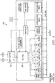
- FIG. 2 is a top-level block diagram illustrating a correlator co-processor system 200 in communication with a pair of slot-aligned IQ buffers 100 while Figure 3 illustrates a more detailed block diagram for the data path portion 300 of the correlator co-processor system 200 depicted in Figure 2 .
- the CCP system 200 when using single or even double data buffers, the CCP system 200 requires four adder trees 302 (2 for on-time and 2 for late-time) for information processing.
- the CCP system 200 requires a single adder tree for on-time and a single adder tree for late-time information processing.
- triple data buffer 100 Without the triple data buffer 100, additional adder trees are necessary to accommodate information processing when the slot timing does not align with the 16-chip processing timing and there is a symbol boundary in the 16 chips.
- Use of triple data buffers was found to reduce overall power requirements associated with correlations over the double buffer feeding additional adder trees.
- the pseudo-noise (PN) generator 304 can also be simplified to one which produces offset spaced 16 apart rather than one which simply produces any offset. Further, logic generally necessary to wrap data around to the beginning of the PN sequence can be eliminated, along with the linear feedback shift register (LFSR) implementation of the PN generator 304, since a window of sequential search hypotheses (+1 advance) no longer requires a PN sequence with the +1 advance feature.
- LFSR linear feedback shift register
- the CCP system 100 hardware must be alerted as to the direction (+/-) and the new sample position. In the worst case condition, extra processing of another 16 chips must be accomplished at the same time as the current 16 chips. Because there is another tree 302 available since the late-time tree is not used for fingers, the number of trees 302 is adequate. Use of the present triple data buffer 100 scheme for the CCP system 100 will operate to retain the foregoing information processing characteristics, even when the first chip being processed is the first chip in the buffer 100 and the timing goes from 0 to 3 (earlier).
- CCP system 100 design is simplified when implemented using the present slot-aligned IQ buffer 100.
- the adder trees 302 can be easily split into one, two, and four results without worry about where the symbol boundary is located.
- coherent adder trees required for space-time transmit diversity (STTD) pilot accumulations was found to be simplified as was pilot de-rotation bit alignments since pilot symbols align within slot and 16-chip windows.
- STTD space-time transmit diversity
- Figure 4 is a diagram illustrating data flow through a series of shift registers 400, 402, 404, suitable to implement a slot-aligned IQ buffer system 100 according to one embodiment of the present invention. Twelve bits of IQ data are communicated to the first buffer 400 and are left shifted until the entire buffer 400 is full. The next IQ data received are then communicated into the next buffer 402 and so on.
- FIG. 5 is a diagram illustrating data flow through a group of load enabled registers 500, 502, 504, suitable to implement a slot-aligned IQ buffer system 100 according to yet another embodiment of the present invention. This embodiment is preferred over the embodiment shown in Figure 4 since this embodiment was found to require lower power to provide a working system. Twelve bits of IQ data are loaded into a desired buffer (register) location. Once loaded, the IQ data does not shift, but remains in its present location until it is read or overwritten. The twelve IQ data lines 510 are connected to each sample register 500, 502, 504 in parallel. A control block 520 enables the proper register 500, 502, 504 in which to load a sequence of data.
- the present invention presents a significant advancement in the art of CDMA and WCDMA information processing.
- a slot-aligned IQ buffer architecture has been implemented to accommodate easy and simple processing of data using minimal hardware resources, even when compressed mode and change of services occur at slot boundaries.
- this invention has been described in considerable detail in order to provide those skilled in the data communication art with the information needed to apply the novel principles and to construct and use such specialized components as are required.
- the present invention represents a significant departure from the prior art in construction and operation.
Landscapes
- Engineering & Computer Science (AREA)
- Computer Networks & Wireless Communication (AREA)
- Signal Processing (AREA)
- Time-Division Multiplex Systems (AREA)
Claims (8)
- IQ-Datenzwischenspeicher mit Schlitzausrichtung (100) für einen Korrelator-Koprozessor, CCP, eines Kommunikationssystems mit einer hohen Bitrate, der Folgendes umfasst:einen ersten Datenzwischenspeicher (102);einen zweiten Datenzwischenspeicher (104); gekennzeichnet durcheinen dritten Datenzwischenspeicher (106);einen ersten Datenmultiplexer (108), der für eine Kommunikation mit dem ersten Datenzwischenspeicher (102), dem zweiten Datenzwischenspeicher (104) und dem dritten Datenzwischenspeicher (106) ausgelegt ist undausgelegt ist, ein Paar Datenzwischenspeicher als Reaktion auf ein gewünschtes Zeitfenster auszusuchen, wobei das ausgewählte Paar Datenzwischenspeicher konfiguriert ist, 16-Chip-breite Vektordaten zu speichern, auf die gleichzeitig während des Speicherns von eingehenden Daten in dem restlichen Datenzwischenspeicher zugegriffen werden kann, um pünktliche und verspätete Datenproben für die Datenverarbeitung an den CCP zu liefern;einen zweiten Datenmultiplexer (110a), der für eine Kommunikation mit dem ersten Datenmultiplexer (108) ausgelegt ist und ausgelegt ist, eine einzige pünktliche Datenprobe als Reaktion auf eine gewünschte Probennummer auszuwählen;einen dritten Datenmultiplexer (110b), der für eine Kommunikation mit dem ersten Datenmultiplexer (108) ausgelegt ist und ausgelegt ist, eine einzige verspätete Datenprobe als Reaktion auf eine gewünschte Probennummer auszuwählen;einen ersten "Barrel-Shifter" (112a), der für eine Kommunikation mit dem zweiten Datenmultiplexer (110a) ausgelegt ist und ausgelegt ist, Chips auszuwählen, die mit eingehenden Rahmen von Daten eine Schlitzausrichtung aufweisen, um pünktliche Datenproben mit Schlitzausrichtung zu erzeugen; undeinen zweiten "Barrel-Shifter" (112b), der für eine Kommunikation mit dem dritten Datenmultiplexer (110b) ausgelegt ist und ausgelegt ist, Chips, die mit eingehenden Rahmen von Daten eine Schlitzausrichtung aufweisen, auszuwählen, um verspätete Datenproben mit Schlitzausrichtung zu erzeugen.
- IQ-Datenzwischenspeicher mit Schlitzausrichtung nach Anspruch 1, wobei jeder Datenzwischenspeicher (102, 104, 106) konfiguriert ist, Signalproben, die 16 Chips von vierfach überabgetasteten phasengleichen Bits und vierfach überabgetasteten Quadraturbits zugeordnet sind, zu speichern.
- IQ-Datenzwischenspeicher mit Schlitzausrichtung nach Anspruch 1, wobei jeder Datenzwischenspeicher (102, 104, 106) konfiguriert ist, 64 Proben von 6 phasengleichen Bits und 64 Proben von 6 Quadraturbits zu speichern.
- IQ-Datenzwischenspeicher mit Schlitzausrichtung nach einem vorhergehenden Anspruch, wobei der erste (102), der zweite (104) und der dritte (106) Datenzwischenspeicher konfiguriert sind, kreisförmig mit eingehenden Daten gefüllt zu werden.
- IQ-Datenzwischenspeicher mit Schlitzausrichtung nach Anspruch 1, wobei der erste Multiplexer (108) ein 3-zu-1-Multiplexer ist.
- IQ-Datenzwischenspeicher mit Schlitzausrichtung nach Anspruch 5, wobei der zweite und der dritte Multiplexer (110a, 110b) 4-zu-1-Multiplexer sind.
- IQ-Datenzwischenspeicher mit Schlitzausrichtung nach Anspruch 2, wobei
der erste Multiplexer (108) konfiguriert ist, einunddreißig vierfach überabgetastete 1/2-Chips innerhalb des gewünschten Zeitfensters auszuwählen;
der zweite Multiplexer (110a) konfiguriert ist, den ersten Multiplexer (108) zu multiplexen, um eine Probe von einunddreißig 1/2-Chips von den einunddreißig vierfach überabgetasteten 1/2-Chips auszuwählen;
der dritte Multiplexer (110b) konfiguriert ist, den ersten Multiplexer (108) zu multiplexen, um eine Probe von einunddreißig 1/2-Chips von den einunddreißig vierfach überabgetasteten 1/2-Chips auszuwählen. - IQ-Datenzwischenspeicher mit Schlitzausrichtung nach Anspruch 7, wobei
der erste "Barrel-Shifter" (112a) konfiguriert ist, Bits, die der durch den zweiten Multiplexer (110a) ausgewählten Probe zugeordnet sind, zu verschieben, um 16 pünktliche Proben mit Schlitzausrichtung zu erzeugen; und
der zweite "Barrel-Shifter" (112b) konfiguriert ist, Bits, die der durch den dritten Multiplexer ausgewählten Probe zugeordnet sind, zu verschieben, um 16 verspätete Proben mit Schlitzausrichtung zu erzeugen.
Applications Claiming Priority (2)
| Application Number | Priority Date | Filing Date | Title |
|---|---|---|---|
| US648184 | 1991-01-31 | ||
| US09/648,184 US6721295B1 (en) | 2000-08-25 | 2000-08-25 | Triple data system for high data rate communication systems |
Publications (3)
| Publication Number | Publication Date |
|---|---|
| EP1182802A2 EP1182802A2 (de) | 2002-02-27 |
| EP1182802A3 EP1182802A3 (de) | 2006-12-13 |
| EP1182802B1 true EP1182802B1 (de) | 2017-04-19 |
Family
ID=24599747
Family Applications (1)
| Application Number | Title | Priority Date | Filing Date |
|---|---|---|---|
| EP01000399.4A Expired - Lifetime EP1182802B1 (de) | 2000-08-25 | 2001-08-22 | Dreifaches Datenpuffersystem für Kommunikationsanordnungen mit Hochdatenraten |
Country Status (2)
| Country | Link |
|---|---|
| US (1) | US6721295B1 (de) |
| EP (1) | EP1182802B1 (de) |
Cited By (1)
| Publication number | Priority date | Publication date | Assignee | Title |
|---|---|---|---|---|
| CN111290305A (zh) * | 2018-12-06 | 2020-06-16 | 航天科工惯性技术有限公司 | 多套惯导系统多路数字量采集与处理防冲突方法及系统 |
Families Citing this family (9)
| Publication number | Priority date | Publication date | Assignee | Title |
|---|---|---|---|---|
| JP2003069517A (ja) * | 2001-08-29 | 2003-03-07 | Fujitsu Ltd | 信号処理装置及び信号処理方法、多重化装置 |
| US7463671B2 (en) * | 2002-02-19 | 2008-12-09 | Marvell World Trade Ltd. | Rake receiver interface |
| US20040071199A1 (en) * | 2002-07-03 | 2004-04-15 | Commasic, Inc. | Virtual finger method and apparatus for processing digital communication signals |
| US7107014B2 (en) * | 2002-10-24 | 2006-09-12 | Nokia Corporation | Transporting power control information |
| US7656905B2 (en) * | 2002-12-24 | 2010-02-02 | Samir Sheth | Apparatus and method for aggregation and transportation of gigabit ethernet and other packet based data formats |
| US7782778B2 (en) * | 2002-12-24 | 2010-08-24 | Samir Satish Sheth | Apparatus and method for fibre channel distance extension embedded within an optical transport system |
| US7243209B2 (en) * | 2005-01-27 | 2007-07-10 | International Business Machines Corporation | Apparatus and method for speeding up access time of a large register file with wrap capability |
| US7577779B2 (en) * | 2006-02-14 | 2009-08-18 | Broadcom Corporation | Method and system for a RFIC master |
| CN111143514B (zh) * | 2019-12-27 | 2023-03-21 | 北京百度网讯科技有限公司 | 用于生成信息的方法和装置 |
Family Cites Families (11)
| Publication number | Priority date | Publication date | Assignee | Title |
|---|---|---|---|---|
| US5710768A (en) | 1994-09-30 | 1998-01-20 | Qualcomm Incorporated | Method of searching for a bursty signal |
| KR100192269B1 (ko) * | 1996-03-25 | 1999-06-15 | 구자홍 | 가변길이 코드 디코더 |
| US6194950B1 (en) * | 1997-08-28 | 2001-02-27 | Lucent Technologies Inc. | High-speed CMOS multiplexer |
| US6366606B1 (en) * | 1998-02-05 | 2002-04-02 | Texas Instruments Incorporated | Programmable correlator coprocessor device and method |
| US6611512B1 (en) * | 1998-10-14 | 2003-08-26 | Agere Systems Inc. | Apparatus and method for scheduling correlation operations of a DS-CDMA shared correlator |
| US6405273B1 (en) * | 1998-11-13 | 2002-06-11 | Infineon Technologies North America Corp. | Data processing device with memory coupling unit |
| US6502152B1 (en) * | 1999-03-08 | 2002-12-31 | Texas Instruments Incorporated | Dual interrupt vector mapping |
| US6473442B1 (en) * | 1999-04-12 | 2002-10-29 | Telefonaktiebolaget Lm Ericsson (Publ) | Communications system and method for matching and balancing the bit rates of transport channels to the bit rate of a physical channel |
| US6404758B1 (en) * | 1999-04-19 | 2002-06-11 | Ericsson, Inc. | System and method for achieving slot synchronization in a wideband CDMA system in the presence of large initial frequency errors |
| KR100390242B1 (ko) * | 1999-06-29 | 2003-07-07 | 주식회사 하이닉스반도체 | 입력 버퍼 |
| US6650694B1 (en) | 2000-02-18 | 2003-11-18 | Texas Instruments Incorporated | Correlator co-processor for CDMA RAKE receiver operations |
-
2000
- 2000-08-25 US US09/648,184 patent/US6721295B1/en not_active Expired - Lifetime
-
2001
- 2001-08-22 EP EP01000399.4A patent/EP1182802B1/de not_active Expired - Lifetime
Non-Patent Citations (1)
| Title |
|---|
| None * |
Cited By (1)
| Publication number | Priority date | Publication date | Assignee | Title |
|---|---|---|---|---|
| CN111290305A (zh) * | 2018-12-06 | 2020-06-16 | 航天科工惯性技术有限公司 | 多套惯导系统多路数字量采集与处理防冲突方法及系统 |
Also Published As
| Publication number | Publication date |
|---|---|
| EP1182802A2 (de) | 2002-02-27 |
| EP1182802A3 (de) | 2006-12-13 |
| US6721295B1 (en) | 2004-04-13 |
Similar Documents
| Publication | Publication Date | Title |
|---|---|---|
| EP1109323B1 (de) | Vorrichtung für die Erzeugung eines kontinuierlichen Stromes von Korrelationswerten | |
| US6459883B2 (en) | Generic finger architecture for spread spectrum applications | |
| JP3415579B2 (ja) | マッチドフィルタおよび相関検出演算方法 | |
| KR100552076B1 (ko) | Cdma통신시스템에있어서의신호수신장치 | |
| US5818868A (en) | Direct-sequence spread-spectrum receiver including code acquisition and detection using an autoadaptive threshold | |
| EP1163731A1 (de) | Sucher mit programmierbarem signalangepasstem filter | |
| AU8895398A (en) | Cell searching in a cdma communications system | |
| EP1182802B1 (de) | Dreifaches Datenpuffersystem für Kommunikationsanordnungen mit Hochdatenraten | |
| US7130331B2 (en) | Method and apparatus for searching time-division multiplexed synchronization sequences | |
| EP1446893B1 (de) | Verfahren und vorrichtungen zur spreizspektrum-signalverarbeitung unter verwendung eines unkonfigurierbaren koprozessors | |
| US6445714B1 (en) | Code generator for multiple correlators | |
| US6014405A (en) | Spread spectrum multipath receiver without a tracking loop | |
| US7027492B2 (en) | Wireless communication system with processor requested RAKE finger tasks | |
| US20050169353A1 (en) | Post despreading interpolation in CDMA systems | |
| JP2002135168A (ja) | Rach受信装置 | |
| US20100002678A1 (en) | Mobile radio terminal and radio communication method | |
| JP3869674B2 (ja) | スペクトラム拡散通信用スライディングコリレータ | |
| KR101157108B1 (ko) | 메모리 아키텍처를 사용하여 1차 셀을 검색하기 위한 상관기 | |
| CA2509161A1 (en) | Memory based device and method for channel estimation in a digital communication receiver | |
| EP1408621A1 (de) | Cdma-empfangsvorrichtung und cdma-empfangsverfahren | |
| KR100327143B1 (ko) | 필요한 고속 가산기의 수가 감소된 cdma 수신기 | |
| KR100313924B1 (ko) | 이동통신 시스템의 신호 검색 장치 및 방법 | |
| EP1306980B1 (de) | Drahtloses Kommunikationssystem mit prozessorgesteuerten Rakefingeraufgaben | |
| AU2776602A (en) | Delay profile measurement for a spread spectrum receiver | |
| JPH11298443A (ja) | 無線受信装置 |
Legal Events
| Date | Code | Title | Description |
|---|---|---|---|
| PUAI | Public reference made under article 153(3) epc to a published international application that has entered the european phase |
Free format text: ORIGINAL CODE: 0009012 |
|
| AK | Designated contracting states |
Kind code of ref document: A2 Designated state(s): AT BE CH CY DE DK ES FI FR GB GR IE IT LI LU MC NL PT SE TR |
|
| AX | Request for extension of the european patent |
Free format text: AL;LT;LV;MK;RO;SI |
|
| PUAL | Search report despatched |
Free format text: ORIGINAL CODE: 0009013 |
|
| AK | Designated contracting states |
Kind code of ref document: A3 Designated state(s): AT BE CH CY DE DK ES FI FR GB GR IE IT LI LU MC NL PT SE TR |
|
| AX | Request for extension of the european patent |
Extension state: AL LT LV MK RO SI |
|
| RIC1 | Information provided on ipc code assigned before grant |
Ipc: H04B 1/707 20060101ALI20061108BHEP Ipc: H04B 7/26 20060101AFI20011023BHEP |
|
| 17P | Request for examination filed |
Effective date: 20070613 |
|
| AKX | Designation fees paid |
Designated state(s): DE FR GB |
|
| 17Q | First examination report despatched |
Effective date: 20090407 |
|
| REG | Reference to a national code |
Ref country code: DE Ref legal event code: R079 Ref document number: 60150399 Country of ref document: DE Free format text: PREVIOUS MAIN CLASS: H04B0007260000 Ipc: H04B0001711500 |
|
| GRAP | Despatch of communication of intention to grant a patent |
Free format text: ORIGINAL CODE: EPIDOSNIGR1 |
|
| RIC1 | Information provided on ipc code assigned before grant |
Ipc: H04B 1/707 20060101ALI20161027BHEP Ipc: H04B 1/7115 20110101AFI20161027BHEP Ipc: H04B 7/26 20060101ALI20161027BHEP |
|
| INTG | Intention to grant announced |
Effective date: 20161123 |
|
| RAP1 | Party data changed (applicant data changed or rights of an application transferred) |
Owner name: TEXAS INSTRUMENTS INC. |
|
| GRAS | Grant fee paid |
Free format text: ORIGINAL CODE: EPIDOSNIGR3 |
|
| GRAA | (expected) grant |
Free format text: ORIGINAL CODE: 0009210 |
|
| AK | Designated contracting states |
Kind code of ref document: B1 Designated state(s): DE FR GB |
|
| REG | Reference to a national code |
Ref country code: GB Ref legal event code: FG4D |
|
| REG | Reference to a national code |
Ref country code: DE Ref legal event code: R096 Ref document number: 60150399 Country of ref document: DE |
|
| REG | Reference to a national code |
Ref country code: FR Ref legal event code: PLFP Year of fee payment: 17 |
|
| PGFP | Annual fee paid to national office [announced via postgrant information from national office to epo] |
Ref country code: GB Payment date: 20170725 Year of fee payment: 17 Ref country code: DE Payment date: 20170825 Year of fee payment: 17 Ref country code: FR Payment date: 20170720 Year of fee payment: 17 |
|
| REG | Reference to a national code |
Ref country code: DE Ref legal event code: R097 Ref document number: 60150399 Country of ref document: DE |
|
| PLBE | No opposition filed within time limit |
Free format text: ORIGINAL CODE: 0009261 |
|
| STAA | Information on the status of an ep patent application or granted ep patent |
Free format text: STATUS: NO OPPOSITION FILED WITHIN TIME LIMIT |
|
| 26N | No opposition filed |
Effective date: 20180122 |
|
| REG | Reference to a national code |
Ref country code: DE Ref legal event code: R119 Ref document number: 60150399 Country of ref document: DE |
|
| GBPC | Gb: european patent ceased through non-payment of renewal fee |
Effective date: 20180822 |
|
| PG25 | Lapsed in a contracting state [announced via postgrant information from national office to epo] |
Ref country code: DE Free format text: LAPSE BECAUSE OF NON-PAYMENT OF DUE FEES Effective date: 20190301 |
|
| PG25 | Lapsed in a contracting state [announced via postgrant information from national office to epo] |
Ref country code: FR Free format text: LAPSE BECAUSE OF NON-PAYMENT OF DUE FEES Effective date: 20180831 |
|
| PG25 | Lapsed in a contracting state [announced via postgrant information from national office to epo] |
Ref country code: GB Free format text: LAPSE BECAUSE OF NON-PAYMENT OF DUE FEES Effective date: 20180822 |