EP1187208A2 - Dispositif semi-conducteur - Google Patents
Dispositif semi-conducteur Download PDFInfo
- Publication number
- EP1187208A2 EP1187208A2 EP01118714A EP01118714A EP1187208A2 EP 1187208 A2 EP1187208 A2 EP 1187208A2 EP 01118714 A EP01118714 A EP 01118714A EP 01118714 A EP01118714 A EP 01118714A EP 1187208 A2 EP1187208 A2 EP 1187208A2
- Authority
- EP
- European Patent Office
- Prior art keywords
- power supply
- pins
- unit amplifiers
- amplifier
- semiconductor device
- Prior art date
- Legal status (The legal status is an assumption and is not a legal conclusion. Google has not performed a legal analysis and makes no representation as to the accuracy of the status listed.)
- Withdrawn
Links
Images



Classifications
-
- H—ELECTRICITY
- H04—ELECTRIC COMMUNICATION TECHNIQUE
- H04B—TRANSMISSION
- H04B1/00—Details of transmission systems, not covered by a single one of groups H04B3/00 - H04B13/00; Details of transmission systems not characterised by the medium used for transmission
- H04B1/005—Details of transmission systems, not covered by a single one of groups H04B3/00 - H04B13/00; Details of transmission systems not characterised by the medium used for transmission adapting radio receivers, transmitters andtransceivers for operation on two or more bands, i.e. frequency ranges
- H04B1/0053—Details of transmission systems, not covered by a single one of groups H04B3/00 - H04B13/00; Details of transmission systems not characterised by the medium used for transmission adapting radio receivers, transmitters andtransceivers for operation on two or more bands, i.e. frequency ranges with common antenna for more than one band
- H04B1/006—Details of transmission systems, not covered by a single one of groups H04B3/00 - H04B13/00; Details of transmission systems not characterised by the medium used for transmission adapting radio receivers, transmitters andtransceivers for operation on two or more bands, i.e. frequency ranges with common antenna for more than one band using switches for selecting the desired band
-
- H—ELECTRICITY
- H03—ELECTRONIC CIRCUITRY
- H03F—AMPLIFIERS
- H03F3/00—Amplifiers with only discharge tubes or only semiconductor devices as amplifying elements
- H03F3/45—Differential amplifiers
-
- H—ELECTRICITY
- H04—ELECTRIC COMMUNICATION TECHNIQUE
- H04B—TRANSMISSION
- H04B1/00—Details of transmission systems, not covered by a single one of groups H04B3/00 - H04B13/00; Details of transmission systems not characterised by the medium used for transmission
- H04B1/005—Details of transmission systems, not covered by a single one of groups H04B3/00 - H04B13/00; Details of transmission systems not characterised by the medium used for transmission adapting radio receivers, transmitters andtransceivers for operation on two or more bands, i.e. frequency ranges
-
- H—ELECTRICITY
- H04—ELECTRIC COMMUNICATION TECHNIQUE
- H04B—TRANSMISSION
- H04B1/00—Details of transmission systems, not covered by a single one of groups H04B3/00 - H04B13/00; Details of transmission systems not characterised by the medium used for transmission
- H04B1/06—Receivers
- H04B1/16—Circuits
- H04B1/26—Circuits for superheterodyne receivers
- H04B1/28—Circuits for superheterodyne receivers the receiver comprising at least one semiconductor device having three or more electrodes
-
- H—ELECTRICITY
- H10—SEMICONDUCTOR DEVICES; ELECTRIC SOLID-STATE DEVICES NOT OTHERWISE PROVIDED FOR
- H10W—GENERIC PACKAGES, INTERCONNECTIONS, CONNECTORS OR OTHER CONSTRUCTIONAL DETAILS OF DEVICES COVERED BY CLASS H10
- H10W44/00—Electrical arrangements for controlling or matching impedance
- H10W44/20—Electrical arrangements for controlling or matching impedance at high-frequency [HF] or radio frequency [RF]
-
- H—ELECTRICITY
- H10—SEMICONDUCTOR DEVICES; ELECTRIC SOLID-STATE DEVICES NOT OTHERWISE PROVIDED FOR
- H10W—GENERIC PACKAGES, INTERCONNECTIONS, CONNECTORS OR OTHER CONSTRUCTIONAL DETAILS OF DEVICES COVERED BY CLASS H10
- H10W72/00—Interconnections or connectors in packages
-
- H—ELECTRICITY
- H10—SEMICONDUCTOR DEVICES; ELECTRIC SOLID-STATE DEVICES NOT OTHERWISE PROVIDED FOR
- H10W—GENERIC PACKAGES, INTERCONNECTIONS, CONNECTORS OR OTHER CONSTRUCTIONAL DETAILS OF DEVICES COVERED BY CLASS H10
- H10W44/00—Electrical arrangements for controlling or matching impedance
- H10W44/20—Electrical arrangements for controlling or matching impedance at high-frequency [HF] or radio frequency [RF]
- H10W44/203—Electrical connections
- H10W44/206—Wires
-
- H—ELECTRICITY
- H10—SEMICONDUCTOR DEVICES; ELECTRIC SOLID-STATE DEVICES NOT OTHERWISE PROVIDED FOR
- H10W—GENERIC PACKAGES, INTERCONNECTIONS, CONNECTORS OR OTHER CONSTRUCTIONAL DETAILS OF DEVICES COVERED BY CLASS H10
- H10W44/00—Electrical arrangements for controlling or matching impedance
- H10W44/20—Electrical arrangements for controlling or matching impedance at high-frequency [HF] or radio frequency [RF]
- H10W44/226—Electrical arrangements for controlling or matching impedance at high-frequency [HF] or radio frequency [RF] for HF amplifiers
-
- H—ELECTRICITY
- H10—SEMICONDUCTOR DEVICES; ELECTRIC SOLID-STATE DEVICES NOT OTHERWISE PROVIDED FOR
- H10W—GENERIC PACKAGES, INTERCONNECTIONS, CONNECTORS OR OTHER CONSTRUCTIONAL DETAILS OF DEVICES COVERED BY CLASS H10
- H10W72/00—Interconnections or connectors in packages
- H10W72/071—Connecting or disconnecting
- H10W72/075—Connecting or disconnecting of bond wires
-
- H—ELECTRICITY
- H10—SEMICONDUCTOR DEVICES; ELECTRIC SOLID-STATE DEVICES NOT OTHERWISE PROVIDED FOR
- H10W—GENERIC PACKAGES, INTERCONNECTIONS, CONNECTORS OR OTHER CONSTRUCTIONAL DETAILS OF DEVICES COVERED BY CLASS H10
- H10W72/00—Interconnections or connectors in packages
- H10W72/50—Bond wires
- H10W72/541—Dispositions of bond wires
- H10W72/5449—Dispositions of bond wires not being orthogonal to a side surface of the chip, e.g. fan-out arrangements
-
- H—ELECTRICITY
- H10—SEMICONDUCTOR DEVICES; ELECTRIC SOLID-STATE DEVICES NOT OTHERWISE PROVIDED FOR
- H10W—GENERIC PACKAGES, INTERCONNECTIONS, CONNECTORS OR OTHER CONSTRUCTIONAL DETAILS OF DEVICES COVERED BY CLASS H10
- H10W72/00—Interconnections or connectors in packages
- H10W72/50—Bond wires
- H10W72/551—Materials of bond wires
-
- H—ELECTRICITY
- H10—SEMICONDUCTOR DEVICES; ELECTRIC SOLID-STATE DEVICES NOT OTHERWISE PROVIDED FOR
- H10W—GENERIC PACKAGES, INTERCONNECTIONS, CONNECTORS OR OTHER CONSTRUCTIONAL DETAILS OF DEVICES COVERED BY CLASS H10
- H10W72/00—Interconnections or connectors in packages
- H10W72/90—Bond pads, in general
- H10W72/951—Materials of bond pads
-
- H—ELECTRICITY
- H10—SEMICONDUCTOR DEVICES; ELECTRIC SOLID-STATE DEVICES NOT OTHERWISE PROVIDED FOR
- H10W—GENERIC PACKAGES, INTERCONNECTIONS, CONNECTORS OR OTHER CONSTRUCTIONAL DETAILS OF DEVICES COVERED BY CLASS H10
- H10W90/00—Package configurations
- H10W90/701—Package configurations characterised by the relative positions of pads or connectors relative to package parts
- H10W90/751—Package configurations characterised by the relative positions of pads or connectors relative to package parts of bond wires
- H10W90/756—Package configurations characterised by the relative positions of pads or connectors relative to package parts of bond wires between a chip and a stacked lead frame, conducting package substrate or heat sink
Definitions
- This invention relates to a transceiver semiconductor device primarily used for wireless communication.
- This invention also relates to USSN 09/547,915 filed Apr. 11, 2001, entitled “SEMICONDUCTOR INTEGRATED CIRCUIT”.
- Fig. 5 of the accompanying drawings shows a structural example of terminal equipment to which a semiconductor integrated circuit for a dual-band wireless transceiver having a built-in differential low-noise amplifier (hereinafter called "transceiver IC”) is applied.
- transceiver IC a semiconductor integrated circuit for a dual-band wireless transceiver having a built-in differential low-noise amplifier
- the transceiver IC 501 is fabricated by incorporating a circuit of a dual-band high frequency part together with a frequency conversion circuit into one chip.
- the IC is connected to a base band IC 515 of a subsequent stage.
- the base band IC executes A/D and D/A conversion of signals, and executes also digital signal processing.
- the transceiver part of the transceiver IC 501 is formed of a low-frequency band differential low-noise amplifier 502a and a low-frequency band reception mixer 503a, a high-frequency band differential low-noise amplifier 502b, a high-frequency band reception mixer 503b, a low-pass filter 504, a variable-gain amplifier 505, a modulator 507 and an offset PLL 508.
- a low-frequency synthesizer 512, a local oscillator 513 and a divider 514 supply a low-frequency local oscillation signal. Since the low-frequency amplifier has a differential construction, single-differential conversion that has been executed by use of a transformer as an external component is not necessary. Therefore, the number of external components can be reduced.
- the differential low-noise amplifier comprises two unit amplifiers having the same construction, and conducts differential amplification by inputting two high-frequency signals having mutually inverse phases.
- transceiver IC having a built-in differential low-noise amplifier
- a RF Transceiver for Digital Wireless Communication in a 25 GHz Bipolar Technology reported by Infineon Co. in ISSCC2000, pp. 144-145 & 451.
- This report describes a transceiver IC for DECT (Digital Enhanced Cordless Telecommunication).
- the low-noise amplifier of the reception system has a differential construction, but signal lines, ground lines, pin arrangement, and so forth, are not known.
- the package used is of a TSSOP38 pin type.
- a typical example of the amplifier in which only the differential amplifier is constituted into an IC is an IF band gain control amplifier, TDA8011T for a satellite TV receiver, a product of Philips Co. (see DATA SHEET, February, 1995).
- the circuit has a differential construction, inputs signals from package pins IF11 and IF12 and outputs them from IFO1 and IFO2.
- a ground pin is one pin.
- Another example is a 1.6 GHz band differential broadband amplifier, ⁇ PC2726T, a product of NEC.
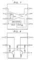
- Fig. 8 shows the pin arrangement and the circuit diagram. The circuit inputs signals from in1 and in2 and outputs them from out1 and out2.
- Fig. 6 is an equivalent circuit diagram representing mutual conductance Gm when an amplifier IC chip is mounted to a package.
- a transistor 601 is a transistor dedicated to the amplifier main body.
- a high-frequency signal is inputted from a base of 602.
- a collector current ic flows when a suitable bias voltage is applied.
- Impedance Ze due to a bonding wire and a pin adds to the emitter of the transistor 601.
- This impedance lowers overall mutual conductance Gm of the amplifier much more than mutual conductance gm of the transistor 601 as represented by equation 601 shown in Fig. 6. Therefore, the number of ground pins is increased and Ze is connected in parallel in an amplifier calling for a high gain. In this way, the inductance component of the bonding wire and the pin can be reduced.
- TABLE 1 shows the pin arrangement of a package, an equivalent circuit and an inductance component when an amplifier has two lead pins (hereinafter called "ground pins") to be connected to a power supply line of a unit amplifier.
- the upper column of TABLE 1 represents the case where the ground pins of the first unit amplifier 101 shown in Fig. 1A are arranged adjacent to each other. Explanation about a circuit using a concrete circuit will be explained in a later-appearing embodiment.
- An input pin IN1 and ground pins G1 and G2 are pins of the first unit amplifier 101.
- Pins IN2, G3 and G4 are pins of the second unit amplifier 106 that forms a pair with the unit amplifier 101.
- Symbol L represents inductance due to the bonding wire and the pins.
- the inductance does not drop to the half even when the ground pin is two pins.
- the inductance is generally about 70% in comparison with the single pin.
- Fig. 1B shows the circuit.
- the ground pins of the unit amplifiers 101 and 106 shown in Fig. 1A change to only G1 and G3.
- a collector current increases when a positive voltage is inputted to the base of a transistor 102 of the first unit amplifier 101 and the voltage drops through a load resistor 105.
- the collector voltage drops and the input signal and the output signal have an inverse phase relation.
- the second unit amplifier 106 Since the input signal has the inverse phase, however, the circuit operations of 101 and 106 have the inverse phase to each other.
- TABLE 2 tabulates the pin arrangement of the package and the emitter impedance of the transistor when the ground pin of the unit amplifier is only one.
- the upper column of this table represents the case where the ground pin G1 of the first unit amplifier 101 shown in Fig. 1b and the input pin IN2 of the second unit amplifier 106 are arranged adjacent to each other. In this case, the pins have the same phase. Therefore, the impedance developing in the emitter of the transistor becomes greater and overall Gm of the amplifier decreases with the drop of the gain.
- the ground pins of the first unit amplifier are arranged adjacent to the ground pins of the second unit amplifier on the 1:1 basis in order to improve the gain of the amplifier.
- the lower column of TABLE 1 illustrates an example of the pin arrangement in one embodiment of the present invention.
- the adjacent pin voltages have inverse phases due to the differential signals.
- the total inductance can be reduced to below the half of the bonding wire and pin inductance.
- the ground pin of the unit amplifier is one pin
- lead pins connected to input lines hereinafter called the "input pins” are arranged adjacent to each other in order to improve the gain of the amplifier.
- the lower column of TABLE 2 illustrates an example of the pin arrangement in one embodiment of the present invention.
- the signals have the inverse phases when the input pin and the ground pin of the same amplifier are arranged adjacent to each other, so that the impedance developing in the emitter of the transistor is smaller.
- Figs. 1A and 1B show a circuit diagram of an embodiment of the present invention.
- the circuit denoted by reference numeral 100 in the drawings is applied to a transceiver IC 501 shown in Fig. 5. More concretely, the circuit 100 shown in Fig. 1A corresponds to a high-frequency band low-noise amplifier 502b and the circuit 100 shown in Fig. 1B corresponds to a low-frequency band low-noise amplifier 502a in Fig. 5.
- a first unit amplifier 101 has a transistor 102, a bias resistor 103 and a load resistor 105.
- the amplifier 101 further includes a bias current supply circuit 104 for supplying a bias.
- Pins of a package are a high-frequency signal input pin IN1 and two ground pins G1 and G2 from an emitter.
- a second unit amplifier 106 forming a pair with the amplifier 101 has the same construction, and includes a transistor 107, a bias resistor 108 and a load resistor 110.
- a bias current supply circuit 109 having the same circuit construction to that of the circuit 104 is likewise disposed. Its package has likewise an input pin IN2 and two ground pins G3 and G4.
- the power supply and the ground pins are a power supply Vcc of the amplifier, a power supply BVcc of the bias circuit and a ground BGND of the bias circuit.
- a differential amplifier having one ground pin in its unit amplifier has the same circuit construction with the exception that the number of pins becomes smaller.
- a high-frequency signal is inputted from an antenna 111.
- a band-pass filter 112 removes out-of-band undesired signals and converts the input signal to differential signals.
- Matching circuits 113 and 114 of a low-noise amplifier establish impedance matching and send the differential signals to a differential low-noise amplifier inside an IC through the pins IN1 and IN2.
- Bias circuits 104 and 109 generate bias currents stable to temperature- and power fluctuation, and determine operation points of the transistors 102 and 107.
- the bias current quantity is equal between the two circuits.
- the bias resistors 103 and 108 convert the bias currents to voltages.
- the differential low-noise amplifier having the construction described above employs the pin arrangement tabulated in the lower column of TABLE 1.
- the ground pins of the first unit amplifier 101 are so arranged adjacent to the ground pins of the second unit amplifier 106 on the 1:1 basis, respectively.
- This arrangement reduces the total inductance to about a half of the bonding wire and pin inductance.
- mutual conductance Gm of the circuit can be increased as represented by equation 601 and the gain can be improved.
- No. 2 in TABLE 4 represents a pin arrangement example in an embodiment of the present invention.
- the circuit analysis tabulated in TABLE 3 and 4 uses a high-frequency simulator HSPICE.
- a bipolar transistor of a 0.35 ⁇ m process is used for the amplifier analyzed.
- a power supply voltage is 2.8 V, and a DC current of 6 mA is caused to flow through the transistors 102 and 107 to operate them.
- Fig. 2 shows a coupling state of pins of a part of the package.
- Reference numeral 201 denotes a part of the package and reference numeral 202 does the pins of the package.
- Symbol k represents a coupling coefficient that determines the quantity of mutual inductance.
- amplifier layout is preferably made in such a way that the low-noise amplifier circuit be disposed at position at which the distance from the distal end of the pin of the emitter of the amplifier transistor to the pad becomes minimal.
- Fig. 3 shows an example of such layout.
- This drawing shows the dual-band transceiver IC described with reference to Fig. 5 by way of example.
- Reference numeral 301 denotes the transceiver IC chip to which the present invention is applied.
- Reference numeral 302 denotes QFP56 pins for sealing the transceiver IC.
- Reference numeral 303 denotes a chip bonding surface of the package.
- Reference numeral 304 denotes a package support.
- Reference numeral 305 denotes a layout position of the high-frequency band differential low-noise amplifier 502b according to the present invention.
- Reference numeral 315 denotes a layout position of the low-frequency band differential low-noise amplifier 502a.
- Reference numerals 306 and 310 denote the ground pins of the transistor 102 shown in Fig. 1A.
- Reference numeral 307 and 311 denote the ground pins of the transistor 107.
- Reference numerals 308 and 309 denote the input pins of the low-noise differential amplifiers 101 and 106, respectively.
- Reference numeral 312 denotes the power supply pin of the high-frequency band low-noise amplifier 502b.
- reference numeral 317 denotes the ground pin of the transistor 102 shown in Fig. 1B
- reference numeral 320 denotes the ground pin of the transistor 107
- reference numerals 318 and 319 denote the input pins of the low-noise differential amplifiers 101 and 106, respectively.
- Reference numeral 316 denotes the power supply pin of the low-frequency band low-noise amplifier 502a.
- Reference numeral 321 denotes the power supply pin of the bias circuit.
- Reference numeral 322 denotes the ground pin of the bias circuit.
- the low-frequency low- noise amplifier and the high-frequency low-noise amplifier share the pins of the bias circuit.
- Reference numeral 323 denotes a bonding wire applied to the lead pin from each pad on the chip.
- the amplifiers are arranged near the center of the end face of the chip and are bonded as shown in the drawing. This arrangement reduces the length of the bonding wires between the pads and the pins. Since this embodiment assumes the dual band, the pins of the amplifiers according to the present invention are allocated to the area extending from the center to the lower end. However, the ground pins 306 and 307 are allocated to the pins at the center. Therefore, the inductance component can be reduced much more than when the amplifiers are arranged at the corners of the chip.
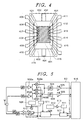
- FIG. 4 shows an example of such an IC.
- Reference numeral 401 denotes a chip of a differential amplifier IC.
- Reference numeral 402 denotes TSSOP 12 pins of a package sealing the differential amplifier IC.
- Reference numeral 403 denotes a chip-bonding surface of the package.
- Reference numeral 404 denotes a package support.
- Reference numerals 405 and 409 denote ground pins of transistor 102.
- Reference numerals 406 and 410 denote ground pins of transistors 107.
- Reference numerals 407 and 408 denote inputs pins of differential amplifiers 101 and 106.
- Reference numeral 411 denotes a power supply pin of a bias circuit.
- Reference numeral 412 denotes a ground pin of a bias circuit.
- Reference numerals 413 and 414 denote output pins of the differential amplifiers.
- Reference numeral 415 denotes a power supply pin of the differential amplifiers.
- Reference numeral 416 denotes a bonding wire put to a lead pin from each pad on the chip.
- Figs. 3 and 4 represent the pin arrangement based on No. 2 of TABLE 3, but the pin arrangement may well be based on the pin arrangement shown in No. 3 of TABLE 3.
- the present invention pertains to the arrangement of the ground pins of the amplifier. Therefore, the present invention can be applied to versatile amplifiers having the differential construction as shown in Fig. 1A.
- the differential amplifier arranges the ground pins of the first unit amplifier adjacent to the ground pins of the second unit amplifier on the 1:1 basis.
- inductance developing in the emitter of each transistor can be reduced to less than half of that of the single ground pin.
- impedance of the emitters of the transistors can be reduced and the gain of the amplifier can be improved.
- the unit amplifier has one ground pin, the ground pin of each amplifier is arranged adjacent to the input pin. According to this arrangement, too, impedance can be reduced and the gain can be improved.
- impedance can be further reduced when the layout in which the low-noise amplifier circuits are disposed at the positions at which the distal end of each pin of the emitter of the amplifier transistor to the pad becomes minimal.
- the improvement of the gain and the symmetrical differential amplifiers inclusive of the influences of the package can be achieved by adding the following two constructions to the present invention.
- the low-noise differential amplifier circuits are disposed at the positions at which the distance from the distal end of each pin of the emitter of the amplifier transistor to the pad becomes minimal.
- a symmetric pin arrangement to the package is employed.
Landscapes
- Engineering & Computer Science (AREA)
- Computer Networks & Wireless Communication (AREA)
- Signal Processing (AREA)
- Power Engineering (AREA)
- Amplifiers (AREA)
- Lead Frames For Integrated Circuits (AREA)
Applications Claiming Priority (2)
| Application Number | Priority Date | Filing Date | Title |
|---|---|---|---|
| JP2000265982 | 2000-08-30 | ||
| JP2000265982A JP4319339B2 (ja) | 2000-08-30 | 2000-08-30 | 半導体装置 |
Publications (2)
| Publication Number | Publication Date |
|---|---|
| EP1187208A2 true EP1187208A2 (fr) | 2002-03-13 |
| EP1187208A3 EP1187208A3 (fr) | 2011-09-07 |
Family
ID=18753157
Family Applications (1)
| Application Number | Title | Priority Date | Filing Date |
|---|---|---|---|
| EP01118714A Withdrawn EP1187208A3 (fr) | 2000-08-30 | 2001-08-03 | Dispositif semi-conducteur |
Country Status (6)
| Country | Link |
|---|---|
| US (1) | US6624509B2 (fr) |
| EP (1) | EP1187208A3 (fr) |
| JP (1) | JP4319339B2 (fr) |
| KR (1) | KR100750449B1 (fr) |
| CN (1) | CN1227733C (fr) |
| TW (1) | TW516268B (fr) |
Cited By (5)
| Publication number | Priority date | Publication date | Assignee | Title |
|---|---|---|---|---|
| WO2003085853A1 (fr) * | 2002-04-08 | 2003-10-16 | Nokia Corporation | Frontal rf polyvalent pour terminaux mobiles multibandes |
| WO2003094232A1 (fr) * | 2002-04-30 | 2003-11-13 | Renesas Technology Corp. | Appareil a semiconducteurs et appareil electronique |
| WO2004073063A1 (fr) * | 2003-02-14 | 2004-08-26 | Renesas Technology Corp. | Dispositif electronique et dispositif a semiconducteur |
| US7312511B2 (en) | 2002-04-30 | 2007-12-25 | Renesas Technology Corp. | Semiconductor device with electrically isolated ground structures |
| CN106936431A (zh) * | 2015-12-30 | 2017-07-07 | 上海贝岭股份有限公司 | 一种高性能低噪音芯片及其制造方法 |
Families Citing this family (18)
| Publication number | Priority date | Publication date | Assignee | Title |
|---|---|---|---|---|
| JP2002076267A (ja) * | 2000-08-22 | 2002-03-15 | Hitachi Ltd | 無線送受信装置 |
| US20020127992A1 (en) * | 2001-03-08 | 2002-09-12 | Fransis Bert L. | Wideband local oscillator architecture |
| US20020127985A1 (en) * | 2001-03-08 | 2002-09-12 | Fransis Bert L. | Wideband local oscillator architecture |
| WO2003094236A1 (fr) * | 2002-04-30 | 2003-11-13 | Renesas Technology Corp. | Dispositif a semi-conducteur et appareil de radiocommunication |
| AU2003234812A1 (en) * | 2002-06-05 | 2003-12-22 | Hitachi Ulsi Systems Co., Ltd. | Semiconductor device |
| KR100499788B1 (ko) * | 2002-11-27 | 2005-07-07 | 인티그런트 테크놀로지즈(주) | 집적회로 칩 |
| TWI225332B (en) * | 2003-05-20 | 2004-12-11 | Mediatek Inc | Multi-band low noise amplifier |
| JP2005006031A (ja) * | 2003-06-11 | 2005-01-06 | Sony Corp | 増幅器および受信回路 |
| KR101014708B1 (ko) * | 2003-08-27 | 2011-02-16 | 엘지전자 주식회사 | 드럼세탁기의 로터리 놉 어셈블리 구조 |
| JP4418250B2 (ja) * | 2004-02-05 | 2010-02-17 | 株式会社ルネサステクノロジ | 高周波回路モジュール |
| JP2006073821A (ja) * | 2004-09-02 | 2006-03-16 | Sharp Corp | 半導体集積回路装置 |
| JP2008218776A (ja) * | 2007-03-06 | 2008-09-18 | Renesas Technology Corp | 半導体装置 |
| US8085596B2 (en) * | 2007-09-11 | 2011-12-27 | Micron Technology, Inc. | Reducing noise in semiconductor devices |
| JP5588147B2 (ja) * | 2009-10-26 | 2014-09-10 | キヤノン株式会社 | 半導体装置及び半導体装置を搭載したプリント基板 |
| JP5499696B2 (ja) * | 2009-12-25 | 2014-05-21 | 富士通セミコンダクター株式会社 | 半導体装置及び実装構造 |
| WO2016185426A1 (fr) * | 2015-05-20 | 2016-11-24 | Wizedsp Ltd. | Amplificateur à faible bruit et à très faible puissance |
| IT201600086488A1 (it) * | 2016-08-22 | 2018-02-22 | St Microelectronics Srl | Dispositivo a semiconduttore e corrispondente procedimento |
| US10880991B2 (en) * | 2018-04-04 | 2020-12-29 | Marvell Asia Pte, Ltd. | Apparatus and methods for enhancing signaling bandwidth in an integrated circuit package |
Family Cites Families (10)
| Publication number | Priority date | Publication date | Assignee | Title |
|---|---|---|---|---|
| JP2716005B2 (ja) * | 1995-07-04 | 1998-02-18 | 日本電気株式会社 | ワイヤボンド型半導体装置 |
| KR0156334B1 (ko) * | 1995-10-14 | 1998-10-15 | 김광호 | 차폐 본딩 와이어를 구비하는 고주파, 고밀도용 반도체 칩 패키지 |
| JPH1075132A (ja) * | 1996-08-29 | 1998-03-17 | Mitsumi Electric Co Ltd | 差動増幅装置 |
| US5789799A (en) * | 1996-09-27 | 1998-08-04 | Northern Telecom Limited | High frequency noise and impedance matched integrated circuits |
| JP3920427B2 (ja) * | 1997-11-19 | 2007-05-30 | 富士通株式会社 | 差動増幅回路及びオペアンプ回路 |
| WO1999027646A1 (fr) * | 1997-11-21 | 1999-06-03 | Hitachi, Ltd. | Dispositif a circuit amplificateur a haute frequence et systeme de transmission a haute frequence comprenant ce dispositif |
| JPH11163644A (ja) * | 1997-11-26 | 1999-06-18 | Fujitsu Ltd | 差動増幅回路の出力回路 |
| US6094084A (en) * | 1998-09-04 | 2000-07-25 | Nortel Networks Corporation | Narrowband LC folded cascode structure |
| JP2000299438A (ja) * | 1999-04-15 | 2000-10-24 | Hitachi Ltd | 半導体集積回路 |
| JP4018312B2 (ja) * | 2000-02-21 | 2007-12-05 | 株式会社ルネサステクノロジ | 無線通信装置 |
-
2000
- 2000-08-30 JP JP2000265982A patent/JP4319339B2/ja not_active Expired - Fee Related
-
2001
- 2001-05-04 TW TW090110764A patent/TW516268B/zh not_active IP Right Cessation
- 2001-07-25 US US09/911,796 patent/US6624509B2/en not_active Expired - Lifetime
- 2001-08-03 EP EP01118714A patent/EP1187208A3/fr not_active Withdrawn
- 2001-08-29 CN CNB011258381A patent/CN1227733C/zh not_active Expired - Fee Related
- 2001-08-30 KR KR1020010052874A patent/KR100750449B1/ko not_active Expired - Fee Related
Cited By (11)
| Publication number | Priority date | Publication date | Assignee | Title |
|---|---|---|---|---|
| WO2003085853A1 (fr) * | 2002-04-08 | 2003-10-16 | Nokia Corporation | Frontal rf polyvalent pour terminaux mobiles multibandes |
| US6751470B1 (en) | 2002-04-08 | 2004-06-15 | Nokia Corporation | Versatile RF front-end multiband mobile terminals |
| WO2003094232A1 (fr) * | 2002-04-30 | 2003-11-13 | Renesas Technology Corp. | Appareil a semiconducteurs et appareil electronique |
| US7312511B2 (en) | 2002-04-30 | 2007-12-25 | Renesas Technology Corp. | Semiconductor device with electrically isolated ground structures |
| US7425756B2 (en) | 2002-04-30 | 2008-09-16 | Renesas Technology Corp. | Semiconductor device and electronic device |
| US7777309B2 (en) | 2002-04-30 | 2010-08-17 | Renesas Technology Corp. | Amplifier chip mounted on a lead frame |
| US7937105B2 (en) | 2002-04-30 | 2011-05-03 | Renesas Electronics Corporation | Semiconductor device and electronic device |
| US8126501B2 (en) | 2002-04-30 | 2012-02-28 | Renesas Electronics Corporation | Semiconductor device and electronic device |
| WO2004073063A1 (fr) * | 2003-02-14 | 2004-08-26 | Renesas Technology Corp. | Dispositif electronique et dispositif a semiconducteur |
| CN106936431A (zh) * | 2015-12-30 | 2017-07-07 | 上海贝岭股份有限公司 | 一种高性能低噪音芯片及其制造方法 |
| CN106936431B (zh) * | 2015-12-30 | 2021-07-20 | 上海贝岭股份有限公司 | 一种高性能低噪音芯片及其制造方法 |
Also Published As
| Publication number | Publication date |
|---|---|
| EP1187208A3 (fr) | 2011-09-07 |
| JP2002076235A (ja) | 2002-03-15 |
| JP4319339B2 (ja) | 2009-08-26 |
| CN1340858A (zh) | 2002-03-20 |
| KR100750449B1 (ko) | 2007-08-22 |
| TW516268B (en) | 2003-01-01 |
| CN1227733C (zh) | 2005-11-16 |
| US20020053729A1 (en) | 2002-05-09 |
| US6624509B2 (en) | 2003-09-23 |
| KR20020018146A (ko) | 2002-03-07 |
Similar Documents
| Publication | Publication Date | Title |
|---|---|---|
| US6624509B2 (en) | Semiconductor device | |
| US6847108B2 (en) | Semiconductor integrated circuit | |
| CN115913142B (zh) | 射频推挽功率放大器芯片及射频前端模组 | |
| US7061329B2 (en) | Semiconductor device having balanced circuit for use in high frequency band | |
| US6162697A (en) | High Q inductor realization for use in MMIC circuits | |
| US20060121875A1 (en) | Wireless communication system | |
| US6169461B1 (en) | High-frequency oscillating circuit | |
| JPH0831750B2 (ja) | Rf増幅器 | |
| KR100372845B1 (ko) | 반도체 장치 | |
| US6768381B2 (en) | Semiconductor power amplifier and multistage monolithic integrated circuit | |
| JP2005184631A (ja) | 高周波電力増幅用電子部品 | |
| US20060043425A1 (en) | Semiconductor integrated circuit device which restricts an increase in the area of a chip, an increase in the number of lead terminals of a package, and can reduce parasitic inductance | |
| US7368996B2 (en) | High frequency power amplifier | |
| US5315156A (en) | Transistor device layout | |
| CN115940830B (zh) | 一种放大电路和包括其的放大器 | |
| KR100499788B1 (ko) | 집적회로 칩 | |
| JP2007259464A (ja) | 半導体集積回路 | |
| JP2001111354A (ja) | ダブルバランス形ミキサ回路 | |
| Vauhkonen et al. | Low power down-conversion RF mixers based on the Gilbert cell approach | |
| JP2004088791A (ja) | 半導体集積回路 | |
| JPH08236691A (ja) | 半導体集積回路装置 |
Legal Events
| Date | Code | Title | Description |
|---|---|---|---|
| PUAI | Public reference made under article 153(3) epc to a published international application that has entered the european phase |
Free format text: ORIGINAL CODE: 0009012 |
|
| AK | Designated contracting states |
Kind code of ref document: A2 Designated state(s): AT BE CH CY DE DK ES FI FR GB GR IE IT LI LU MC NL PT SE TR |
|
| AX | Request for extension of the european patent |
Free format text: AL;LT;LV;MK;RO;SI |
|
| PUAL | Search report despatched |
Free format text: ORIGINAL CODE: 0009013 |
|
| AK | Designated contracting states |
Kind code of ref document: A3 Designated state(s): AT BE CH CY DE DK ES FI FR GB GR IE IT LI LU MC NL PT SE TR |
|
| AX | Request for extension of the european patent |
Extension state: AL LT LV MK RO SI |
|
| RIC1 | Information provided on ipc code assigned before grant |
Ipc: H01L 23/66 20060101AFI20110802BHEP |
|
| AKX | Designation fees paid |
Designated state(s): DE FR GB IT |
|
| STAA | Information on the status of an ep patent application or granted ep patent |
Free format text: STATUS: THE APPLICATION IS DEEMED TO BE WITHDRAWN |
|
| 18D | Application deemed to be withdrawn |
Effective date: 20120308 |