EP1187332A2 - Circuit diviseur de fréquence - Google Patents
Circuit diviseur de fréquence Download PDFInfo
- Publication number
- EP1187332A2 EP1187332A2 EP01119046A EP01119046A EP1187332A2 EP 1187332 A2 EP1187332 A2 EP 1187332A2 EP 01119046 A EP01119046 A EP 01119046A EP 01119046 A EP01119046 A EP 01119046A EP 1187332 A2 EP1187332 A2 EP 1187332A2
- Authority
- EP
- European Patent Office
- Prior art keywords
- frequency divider
- signal
- divider circuit
- output
- differential amplifier
- Prior art date
- Legal status (The legal status is an assumption and is not a legal conclusion. Google has not performed a legal analysis and makes no representation as to the accuracy of the status listed.)
- Withdrawn
Links
Images


Classifications
-
- H—ELECTRICITY
- H03—ELECTRONIC CIRCUITRY
- H03K—PULSE TECHNIQUE
- H03K3/00—Circuits for generating electric pulses; Monostable, bistable or multistable circuits
- H03K3/01—Details
- H03K3/012—Modifications of generator to improve response time or to decrease power consumption
-
- H—ELECTRICITY
- H03—ELECTRONIC CIRCUITRY
- H03K—PULSE TECHNIQUE
- H03K3/00—Circuits for generating electric pulses; Monostable, bistable or multistable circuits
- H03K3/02—Generators characterised by the type of circuit or by the means used for producing pulses
- H03K3/26—Generators characterised by the type of circuit or by the means used for producing pulses by the use, as active elements, of bipolar transistors with internal or external positive feedback
- H03K3/28—Generators characterised by the type of circuit or by the means used for producing pulses by the use, as active elements, of bipolar transistors with internal or external positive feedback using means other than a transformer for feedback
- H03K3/281—Generators characterised by the type of circuit or by the means used for producing pulses by the use, as active elements, of bipolar transistors with internal or external positive feedback using means other than a transformer for feedback using at least two transistors so coupled that the input of one is derived from the output of another, e.g. multivibrator
- H03K3/286—Generators characterised by the type of circuit or by the means used for producing pulses by the use, as active elements, of bipolar transistors with internal or external positive feedback using means other than a transformer for feedback using at least two transistors so coupled that the input of one is derived from the output of another, e.g. multivibrator bistable
- H03K3/288—Generators characterised by the type of circuit or by the means used for producing pulses by the use, as active elements, of bipolar transistors with internal or external positive feedback using means other than a transformer for feedback using at least two transistors so coupled that the input of one is derived from the output of another, e.g. multivibrator bistable using additional transistors in the input circuit
- H03K3/2885—Generators characterised by the type of circuit or by the means used for producing pulses by the use, as active elements, of bipolar transistors with internal or external positive feedback using means other than a transformer for feedback using at least two transistors so coupled that the input of one is derived from the output of another, e.g. multivibrator bistable using additional transistors in the input circuit the input circuit having a differential configuration
Definitions
- the present invention relates to a frequency divider circuit.
- Frequency dividers are digital circuits in which the input frequencies integer multiples of the output frequencies are.
- the simplest frequency divider consists of a bistable T-flip-flop, which is the input frequency in relation 2: 1 divides.
- Frequency dividers with master-slave flip-flops are usually used realized.
- Such a frequency divider circuit is for example from Tietze, Schenk: semiconductor circuit technology, 10th edition, pages 235 to 240 known.
- these known frequency divider circuits at least three transistor levels between two supply potentials arranged one above the other so that to supply such known frequency divider circuits are proportionate large supply voltages required and only relative small signal amplitudes can be achieved.
- the object of the present invention is a frequency divider circuit specify which for low supply voltages is suitable and can be achieved with the large signal amplitudes are.
- the frequency divider circuit described has two differential amplifiers depending on the clock input signal one is active at a time.
- the one at the main respectively Auxiliary output derivable clock output signals can have a phase shift of 90 ° to one another.
- Differential amplifiers are required, this is low Power requirements realizable.
- the first differential amplifier has means for providing it an inverted signal and the second differential amplifier Means for providing a non-inverted Signal on.
- the first differential amplifier sets the output side of the main output on the input side applied signal of the auxiliary output is inverted ready.
- the second differential amplifier is on the output side Auxiliary output the signal of the main output on the input side ready non-inverted.
- First and second differential amplifiers are dependent on the clock input signal alternately active.
- the means to invert or non-invert the signals can then be carried out in a particularly simple manner be, for example by reversing the polarity of connection pairs, if the clock output signals are present as differential signals and main and auxiliary output, each with a corresponding connection pair are realized.
- the frequency divider circuit have the differential amplifier means to hold a signal on the input side. additionally to provide an inverted or non-inverted signal can be the differential amplifier Means for holding the signal present on the input side exhibit.
- the first differential amplifier holds that Clock output signal, which is present at the auxiliary output, and the second differential amplifier holds the one at the main output Clock output. If the differential amplifier without additional Wiring have inverting properties, see above the means for holding can then be implemented particularly easily be when the clock output signals as differential signals available.
- first and second differential amplifiers to a current source that can be switched with the clock input signal connected.
- the power sources can be first and second Differential amplifier alternating depending on the clock input signal activate.
- the frequency divider circuit with switchable Current sources have a particularly simple circuit structure on.
- the current sources can be connected to the reference potential Differential amplifiers can be connected, resulting in a extensive independence of the circuit properties from Fluctuations in the supply voltage, which the frequency divider circuit supplied, results.
- first and second differential amplifiers to one emitter follower that can be switched with the clock input signal connected. This allows the differential amplifiers switch off particularly quickly, which has steep slopes which enables clock output signals. It is also suitable this embodiment for particularly low supply voltages and large signal amplitudes at the output.
- the invention is on the input side of the differential amplifiers one emitter follower each for coupling with main or Auxiliary output connected. This allows the amplitudes of the clock output signal can be further increased. Farther there is an even greater slope, which reduces the phase noise of the frequency divider circuit.
- the emitter followers act as impedance converters.
- the differential amplifiers each have four emitter-coupled ones npn transistors, whose emitter connections are coupled to the input.
- the four emitter-coupled Transistors can have two emitter-coupled transistors to provide the inverted respectively non-inverted signal on the output side at the differential amplifiers be provided and two more, emitter-coupled Transistors can be used to hold an input on the Differential amplifier applied signal can be provided.
- the clock input signal to the emitter connections of the transistors of the first differential amplifier non-inverted and the emitter terminals of the transistors of the second differential amplifier can be supplied inverted.
- Figure 1 shows a frequency divider circuit with an input C, CX, which is connected to current sources S1, S2 to control them is.
- the switchable current sources S1, S2 are switched on Clock input signal on the one hand non-inverted and on the other others fed inverted.
- the switchable power sources S1, S2 are each connected to a common emitter line of the first Differential amplifier DV1 or the second Differential amplifier DV2 connected.
- first Differential amplifier DV1 from the non-inverted applied to input C.
- Clock input signal and the second differential amplifier DV2 from the inverted applied to input CX Clock input signal driven. So first and second are Differential amplifier DV1, DV2 depending on the clock input signal alternately active.
- the first differential amplifier DV1 is on the input side with the Auxiliary output Q, QX and output side via a first pair of transistors T1, T3 connected to the main output I, IX in such a way that when the first differential amplifier DV1 is active at the main output I, IX the inverted signal of the at the auxiliary output Q, QX applied signal is formed.
- a second pair of transistors T5 of the first differential amplifier DV1 is one Latching of the signal present at the auxiliary output Q, QX formed when the first differential amplifier DV1 is active.
- the frequency divider circuit has only two differential amplifiers DV1, DV2 and is with low supply voltage operable, since only a few transistor levels are provided are. There is a signal at each of the outputs Q, QX, I, IX with half the frequency that can be applied to the clock signal input C, CX Derived signal, which has large signal amplitudes.
- the frequency divider circuit described has a low one Power requirements. Because there is a phase shift between the clock output signals is given by 90 degrees, the frequency divider circuit for example integrated in receiver circuits be in which one of in-phase and quadrature components existing carrier signal is required.
- FIG 2 shows a development of the frequency divider circuit according to Figure 1, in which instead of at the emitter node first and second differential amplifiers DV1, DV2 connected, switchable current sources S1, S2 for on and turn off the first and second differential amplifier DV1, DV2 each have an emitter follower T7, T8 is.
- the emitter nodes are each connected to current sources S connected, which with a connection for a reference potential are connected.
- the one designed as a bipolar transistor Emitter follower T7 is at its base terminal with the clock signal input C, with its emitter connection with the common one Emitter connection of the first differential amplifier DV1 and with its collector connection connected to the supply connection VCC.
- the emitter follower T8 with its Base connection with the clock signal input CX, with its emitter connection with the common emitter connection of the second Differential amplifier DV2 and with its collector connection with connected to the supply connection VCC.
- the frequency divider circuit described enables operation with a particularly low supply voltage and enables particularly large signal amplitudes at the for outputs I, IX, Q, QX.
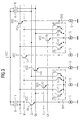
- FIG. 3 shows a third exemplary embodiment of the frequency divider circuit, which is a further development of the frequency divider circuit of Figure 2 corresponds.
- the base connections of the emitter followers T9, T10, T11, T12 are each with the corresponding main or Auxiliary outputs Q, QX, I, IX connected while the Emitter connections of the emitter followers T9 to T12 each with the base connections of the transistors T1 to T6 of the differential amplifier DV1, DV2 are connected, which additionally connected to the reference potential via a current source S. are.
- the frequency divider circuit according to Figure 3 with the additional Emitter followers T9 to T12 enable even larger ones Signal amplitudes at the main and auxiliary outputs I, IX, Q, QX because the emitter followers T9 to T12 have higher currents available on the input side at the differential amplifiers DV1, DV2 can put.
- the higher edge steepness at Frequency divider circuit according to Figure 3 leads to a very low Phase noise of the frequency divider.
- frequency divider circuit can also use pnp transistors instead of the described npn transistors or field effect transistors can be used.
- pnp transistors instead of the described npn transistors or field effect transistors can be used.
- emitter followers described To provide source followers instead of the emitter followers described To provide source followers.
- the frequency divider circuits described are only with two differential amplifiers can be implemented and consequently have a low power requirement.
- the current sources S as well the switchable current sources S1, S2, each on the reference potential side or are provided on the ground side, enable operation of the frequency divider circuit, the largely independent of supply voltage fluctuations is.
- Figure 4 finally explains the function of the frequency divider circuits according to Figures 1 to 3 based on the waveforms of the signals at the clock signal input C and at the main and Auxiliary output I, Q.
- the signal that can be derived at the main output I, IX is in Phase to the clock input signal, while that at the auxiliary output Q, QX derivable signal shows a phase shift of 90 °.
- first differential amplifier DV1 active.
- second and fourth cycle phases II, IV is the inverted of the one not shown here Clock signal CX driven, second differential amplifier DV2 active.
- the first differential amplifier DV1 forms on the output side, that is, the inverted one at the main output I. Signal of the signal present at auxiliary output Q.
- the second Differential amplifier DV2 forms on the output side, that is on Auxiliary output Q each the non-inverted signal of the am Main output I applied signal.
Landscapes
- Engineering & Computer Science (AREA)
- Power Engineering (AREA)
- Amplifiers (AREA)
- Manipulation Of Pulses (AREA)
Applications Claiming Priority (2)
| Application Number | Priority Date | Filing Date | Title |
|---|---|---|---|
| DE10043953 | 2000-09-06 | ||
| DE10043953A DE10043953C2 (de) | 2000-09-06 | 2000-09-06 | Frequenzteilerschaltung |
Publications (2)
| Publication Number | Publication Date |
|---|---|
| EP1187332A2 true EP1187332A2 (fr) | 2002-03-13 |
| EP1187332A3 EP1187332A3 (fr) | 2003-10-01 |
Family
ID=7655205
Family Applications (1)
| Application Number | Title | Priority Date | Filing Date |
|---|---|---|---|
| EP01119046A Withdrawn EP1187332A3 (fr) | 2000-09-06 | 2001-08-07 | Circuit diviseur de fréquence |
Country Status (3)
| Country | Link |
|---|---|
| US (1) | US6545517B2 (fr) |
| EP (1) | EP1187332A3 (fr) |
| DE (1) | DE10043953C2 (fr) |
Cited By (1)
| Publication number | Priority date | Publication date | Assignee | Title |
|---|---|---|---|---|
| CN102594297A (zh) * | 2011-01-12 | 2012-07-18 | 三美电机株式会社 | 振荡电路 |
Families Citing this family (7)
| Publication number | Priority date | Publication date | Assignee | Title |
|---|---|---|---|---|
| TW595174B (en) * | 2002-08-28 | 2004-06-21 | Novatek Microelectronics Corp | Signal frequency splitter and frequency shift key decoding apparatus using the same |
| DE10313332A1 (de) * | 2003-03-25 | 2004-10-21 | Infineon Technologies Ag | Frequenzteiler-Anordnung mit Stromsignaleinpeisung |
| DE10319089B4 (de) * | 2003-04-28 | 2008-05-29 | Austriamicrosystems Ag | Flip-Flop-Schaltungsanordnung |
| JP4246166B2 (ja) * | 2004-03-04 | 2009-04-02 | パナソニック株式会社 | 分周回路及びそれを用いたマルチモード無線機 |
| US7348818B2 (en) * | 2005-06-30 | 2008-03-25 | Silicon Laboratories Inc. | Tunable high-speed frequency divider |
| JP4334564B2 (ja) * | 2006-12-14 | 2009-09-30 | 株式会社東芝 | トランスコンダクタ |
| DE112015007105T5 (de) * | 2015-12-11 | 2018-08-02 | Gm Global Technology Operations, Llc | Aktive quadraturschaltungen für hochfrequenzanwendungen |
Family Cites Families (7)
| Publication number | Priority date | Publication date | Assignee | Title |
|---|---|---|---|---|
| DE3343573A1 (de) * | 1983-12-01 | 1985-06-13 | Siemens AG, 1000 Berlin und 8000 München | Integrierbare halbleiterschaltung fuer einen frequenzteiler |
| JP2913670B2 (ja) * | 1989-06-19 | 1999-06-28 | 日本電気株式会社 | 分周回路 |
| JPH04274616A (ja) * | 1991-03-01 | 1992-09-30 | Nippon Telegr & Teleph Corp <Ntt> | Cmosスタティック型可変分周回路 |
| JP2947494B2 (ja) * | 1992-05-13 | 1999-09-13 | 三菱電機株式会社 | Ecl回路 |
| JP3350337B2 (ja) * | 1996-03-08 | 2002-11-25 | 株式会社東芝 | 分周器 |
| JP3631375B2 (ja) * | 1998-06-30 | 2005-03-23 | 株式会社東芝 | 分周器 |
| US6140845A (en) * | 1998-12-04 | 2000-10-31 | The Texas A&M University System | Pseudo-dynamic differential flip-flop |
-
2000
- 2000-09-06 DE DE10043953A patent/DE10043953C2/de not_active Expired - Fee Related
-
2001
- 2001-08-07 EP EP01119046A patent/EP1187332A3/fr not_active Withdrawn
- 2001-09-06 US US09/948,260 patent/US6545517B2/en not_active Expired - Lifetime
Cited By (2)
| Publication number | Priority date | Publication date | Assignee | Title |
|---|---|---|---|---|
| CN102594297A (zh) * | 2011-01-12 | 2012-07-18 | 三美电机株式会社 | 振荡电路 |
| CN102594297B (zh) * | 2011-01-12 | 2016-01-27 | 三美电机株式会社 | 振荡电路 |
Also Published As
| Publication number | Publication date |
|---|---|
| DE10043953A1 (de) | 2002-03-14 |
| DE10043953C2 (de) | 2002-08-01 |
| EP1187332A3 (fr) | 2003-10-01 |
| US6545517B2 (en) | 2003-04-08 |
| US20020067191A1 (en) | 2002-06-06 |
Similar Documents
| Publication | Publication Date | Title |
|---|---|---|
| DE69422010T2 (de) | Phasenschiebverstärker und seine Verwendung in einer Zusammenführungsschaltung | |
| EP1189337B1 (fr) | Circuit mélangeur équilibré utilisant transistors bipolaires | |
| DE10232861A1 (de) | Frequenzverdoppler-Schaltungsanordnung | |
| EP0417334B1 (fr) | Circuit de bascule avec hystérésis de commutation | |
| EP1187332A2 (fr) | Circuit diviseur de fréquence | |
| DE69418644T2 (de) | Verstärkeranordnungen für einen integrierten Schaltkreis | |
| DE102004058409B4 (de) | Master-Slave Flip-Flop und dessen Verwendung | |
| DE69319553T2 (de) | Eintakt-in-Gegentakt-Umwandler | |
| DE102004058300B4 (de) | Schaltungsanordnung zur Erzeugung eines komplexen Signals und Verwendung in einem Hochfrequenz-Sender oder -Empfänger | |
| EP0077500A2 (fr) | Diviseur de fréquence intégrable | |
| DE2528424A1 (de) | Differenzverstaerker | |
| DE2944034C2 (de) | Flip-Flop-Schaltung sowie damit ausgerüstete Frequenzteilerschaltung | |
| DE2524044C3 (de) | Universelles Verknüpfungsglied für den Subnanosekundenbereich | |
| EP1618665B1 (fr) | Ensemble bascule | |
| DE69118249T2 (de) | Verriegelschaltung | |
| EP0421016A1 (fr) | Convertisseur de niveau ECL-TTL | |
| EP0429717B1 (fr) | Amplificateur de transconductance | |
| EP0133618A1 (fr) | Circuit oscillateur haute fréquence à quartz sous forme de circuit intégré monolithique | |
| EP0691734B1 (fr) | Circuit amplificateur pour signaux à haute fréquence | |
| EP0246689B1 (fr) | Circuit pour convertir des signaux à trois états en signaux binaires | |
| EP1122680A1 (fr) | Multiplicateur analogique | |
| EP0448834B1 (fr) | Circuit flip-flop intégré | |
| DE10038905A1 (de) | Verfahren zur Erhöhung der Grenzfrequenz bei Flip-Flops | |
| EP0586730B1 (fr) | Circuit pour transformer un signal d'entrée symmétrique biphasé en un signal de sortie asymmétrique monophasé | |
| DE4001573C2 (fr) |
Legal Events
| Date | Code | Title | Description |
|---|---|---|---|
| PUAI | Public reference made under article 153(3) epc to a published international application that has entered the european phase |
Free format text: ORIGINAL CODE: 0009012 |
|
| AK | Designated contracting states |
Kind code of ref document: A2 Designated state(s): AT BE CH CY DE DK ES FI FR GB GR IE IT LI LU MC NL PT SE TR |
|
| AX | Request for extension of the european patent |
Free format text: AL;LT;LV;MK;RO;SI |
|
| PUAL | Search report despatched |
Free format text: ORIGINAL CODE: 0009013 |
|
| AK | Designated contracting states |
Kind code of ref document: A3 Designated state(s): AT BE CH CY DE DK ES FI FR GB GR IE IT LI LU MC NL PT SE TR |
|
| AX | Request for extension of the european patent |
Extension state: AL LT LV MK RO SI |
|
| 17P | Request for examination filed |
Effective date: 20040326 |
|
| AKX | Designation fees paid |
Designated state(s): DE FR GB |
|
| 17Q | First examination report despatched |
Effective date: 20080814 |
|
| RAP1 | Party data changed (applicant data changed or rights of an application transferred) |
Owner name: INFINEON TECHNOLOGIES AG |
|
| STAA | Information on the status of an ep patent application or granted ep patent |
Free format text: STATUS: THE APPLICATION IS DEEMED TO BE WITHDRAWN |
|
| 18D | Application deemed to be withdrawn |
Effective date: 20100302 |