EP1188246B1 - Reprogrammierbare digitale drahtlose Vorrichtung und Verfahren zur Nutzung derselben - Google Patents
Reprogrammierbare digitale drahtlose Vorrichtung und Verfahren zur Nutzung derselben Download PDFInfo
- Publication number
- EP1188246B1 EP1188246B1 EP00935875A EP00935875A EP1188246B1 EP 1188246 B1 EP1188246 B1 EP 1188246B1 EP 00935875 A EP00935875 A EP 00935875A EP 00935875 A EP00935875 A EP 00935875A EP 1188246 B1 EP1188246 B1 EP 1188246B1
- Authority
- EP
- European Patent Office
- Prior art keywords
- software
- reconfigurable
- wireless communication
- processor
- heterogeneous
- Prior art date
- Legal status (The legal status is an assumption and is not a legal conclusion. Google has not performed a legal analysis and makes no representation as to the accuracy of the status listed.)
- Expired - Lifetime
Links
- 238000004891 communication Methods 0.000 title claims abstract description 47
- 238000000034 method Methods 0.000 title claims abstract description 17
- 238000012545 processing Methods 0.000 claims abstract description 58
- 230000006870 function Effects 0.000 claims description 33
- 230000008859 change Effects 0.000 claims description 5
- 238000004519 manufacturing process Methods 0.000 claims description 3
- 238000012356 Product development Methods 0.000 abstract description 4
- 230000003416 augmentation Effects 0.000 abstract description 2
- 238000004458 analytical method Methods 0.000 description 6
- 239000011159 matrix material Substances 0.000 description 6
- 238000013459 approach Methods 0.000 description 5
- 238000001514 detection method Methods 0.000 description 5
- 238000001914 filtration Methods 0.000 description 4
- 230000003068 static effect Effects 0.000 description 4
- 230000003190 augmentative effect Effects 0.000 description 3
- 238000006243 chemical reaction Methods 0.000 description 3
- 230000001419 dependent effect Effects 0.000 description 3
- 230000007246 mechanism Effects 0.000 description 3
- 238000011217 control strategy Methods 0.000 description 2
- 238000013461 design Methods 0.000 description 2
- 238000007726 management method Methods 0.000 description 2
- 238000013507 mapping Methods 0.000 description 2
- 230000006855 networking Effects 0.000 description 2
- 239000007993 MOPS buffer Substances 0.000 description 1
- XUIMIQQOPSSXEZ-UHFFFAOYSA-N Silicon Chemical compound [Si] XUIMIQQOPSSXEZ-UHFFFAOYSA-N 0.000 description 1
- 230000005540 biological transmission Effects 0.000 description 1
- 238000012512 characterization method Methods 0.000 description 1
- 230000003750 conditioning effect Effects 0.000 description 1
- 239000000470 constituent Substances 0.000 description 1
- 238000010586 diagram Methods 0.000 description 1
- 230000000694 effects Effects 0.000 description 1
- 239000000203 mixture Substances 0.000 description 1
- 238000012986 modification Methods 0.000 description 1
- 230000004048 modification Effects 0.000 description 1
- 230000002093 peripheral effect Effects 0.000 description 1
- 230000010076 replication Effects 0.000 description 1
- 238000011160 research Methods 0.000 description 1
- 229910052710 silicon Inorganic materials 0.000 description 1
- 239000010703 silicon Substances 0.000 description 1
- 239000000243 solution Substances 0.000 description 1
- 238000000638 solvent extraction Methods 0.000 description 1
- 230000002123 temporal effect Effects 0.000 description 1
Images


Classifications
-
- H—ELECTRICITY
- H04—ELECTRIC COMMUNICATION TECHNIQUE
- H04B—TRANSMISSION
- H04B1/00—Details of transmission systems, not covered by a single one of groups H04B3/00 - H04B13/00; Details of transmission systems not characterised by the medium used for transmission
- H04B1/06—Receivers
- H04B1/16—Circuits
- H04B1/26—Circuits for superheterodyne receivers
-
- H—ELECTRICITY
- H04—ELECTRIC COMMUNICATION TECHNIQUE
- H04B—TRANSMISSION
- H04B1/00—Details of transmission systems, not covered by a single one of groups H04B3/00 - H04B13/00; Details of transmission systems not characterised by the medium used for transmission
- H04B1/0003—Software-defined radio [SDR] systems, i.e. systems wherein components typically implemented in hardware, e.g. filters or modulators/demodulators, are implented using software, e.g. by involving an AD or DA conversion stage such that at least part of the signal processing is performed in the digital domain
-
- H—ELECTRICITY
- H04—ELECTRIC COMMUNICATION TECHNIQUE
- H04B—TRANSMISSION
- H04B1/00—Details of transmission systems, not covered by a single one of groups H04B3/00 - H04B13/00; Details of transmission systems not characterised by the medium used for transmission
- H04B1/005—Details of transmission systems, not covered by a single one of groups H04B3/00 - H04B13/00; Details of transmission systems not characterised by the medium used for transmission adapting radio receivers, transmitters andtransceivers for operation on two or more bands, i.e. frequency ranges
-
- H—ELECTRICITY
- H04—ELECTRIC COMMUNICATION TECHNIQUE
- H04B—TRANSMISSION
- H04B1/00—Details of transmission systems, not covered by a single one of groups H04B3/00 - H04B13/00; Details of transmission systems not characterised by the medium used for transmission
- H04B1/06—Receivers
- H04B1/16—Circuits
- H04B1/26—Circuits for superheterodyne receivers
- H04B1/28—Circuits for superheterodyne receivers the receiver comprising at least one semiconductor device having three or more electrodes
-
- H—ELECTRICITY
- H04—ELECTRIC COMMUNICATION TECHNIQUE
- H04B—TRANSMISSION
- H04B1/00—Details of transmission systems, not covered by a single one of groups H04B3/00 - H04B13/00; Details of transmission systems not characterised by the medium used for transmission
Definitions
- This invention relates generally to wireless communication devices. More particularly, this invention relates to a reconfigurable digital wireless communication device.
- Existing communication devices are "static" devices. That is, they are designed to support a specific wireless communication standard and/or to support a specific application (e.g., voice, data transmission) at a specific data rate.
- a specific application e.g., voice, data transmission
- different wireless communication standards are used in different wireless networks, both within a geographic locality and worldwide. Thus, an individual traveling between different regions is required to use a separate wireless communication device in each region.
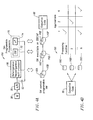
- FIG. 1 illustrates a digital communication modem 20 that may be implemented in accordance with prior art approaches to multi-standard communication devices.
- a transmitter 22 transmits a signal to a channel 24, which may be a wireless or physical channel.
- the transmitted signal is received at the modem 20, where it is initially processed by a Radio Frequency (RF) subsystem 26.
- the RF subsystem 26 performs analog mixing, analog filtering, and analog gain control functions.
- the analog signal from the RF subsystem 26 is then converted to an equivalent digital signal by an analog-to-digital converter 28.
- RF Radio Frequency
- the digital signal is then processed by a digital front-end processing circuit 30, which performs standard-specific, channel-specific, and modulation-specific bandwidth selection, filtering, sampling-rate control and other signal processing.
- the signal from the digital front-end processing circuit 30 is then passed to a detector/demodulator circuit 32, which performs signal detection and demodulation operations.
- the detection and demodulation circuit 32 also interacts with a parameter estimation circuit 34.
- the output from the detection and demodulation circuit 32 is subsequently processed by a channel decoder 36 and then a source decoder 38.
- FIG 2A shows a prior art architecture for implementing the structure of Figure 1 .
- An RF subsystem 26 is again used to provide one or more bandpass signals (intermediate frequency signals), which are then digitized by the analog-to-digital converter 28, which is typically implemented as a free-running analog-to-digital converter.
- the output from the analog-to-digital converter 28 is placed on a bus 52.
- Signals from the bus 52 are routed to hardware processors 60 and software programmable processors 70.
- the hardware processors include programmable logic device 62 and fixed-function logic 64.
- the software programmable processors include digital signal processor 72 and microprocessor 74.
- the digital components (30, 32, 34, 36, and 38) of the device 20 are typically implemented on software-programmable processors 70, or as a fully hardwired, non-programmable application-specific integrated circuit 64.
- the hardwired circuit may be augmented by a programmable logic device 62, which provides limited fine-granularity programmability.
- the device 50 of Figure 2A facilitates the management of functions executing on the programmable logic device 62 via controlling the download of functionality into the programmable logic device 62 and control of the dataflow into and out of the programmable logic device 62.
- the software-programmable processors 70 typically comprises a digital signal processor 72 and a control microprocessor 74.
- the signal processing device 50 can be highly optimized only for a particular communication standard, service and application.
- Prior art approaches to accommodating multiple standards, services and applications have essentially consisted of combining the disparate hardware and software resources separately optimized for each service of interest. This results in poor efficiency in terms of size, weight and power consumption.
- FIG. 2B illustrates the control architecture 80 for a prior art multi-standard communication apparatus.
- the architecture 80 includes executive code 88, which is effectively an operating system running on microprocessor 74 or digital signal processor 72.
- One of a suite of applications 84 is selected to run under the operating system.
- Each application 84 executes a set of software/hardware functions 82A-C.
- Each application 84 requires computation resources, which are available according to Figure 2A , either via a microprocessor, a digital signal processor, a fixed-function logic engine, or a programmable logic engine. Thus, each of the applications requires some combination of these resources; the actual partitioning among their use is determined by the product/application requirements.
- a general microprocessor core (most of the time only one of these is sufficient), a dedicated functional module such as a multiply-accumulator or a DCT unit, an embedded memory, a reconfigurable datapath or an embedded PGA.
- Each of the satellite processors has its own autonomous controller, although the instruction set of most of these modules is very shallow.
- the microprocessor core configures the satellite processors and the communication network over the reconfiguration bus and manages the overall control flow of the application, either in a static compiled order or through a dynamic real-time kernel.
- a digital wireless communication device comprises a software-programmable processor, a heterogeneous reconfigurable multiprocessing logic circuit, and a bus connecting the software-programmable processor and the heterogeneous reconfigurable multiprocessing logic circuit.
- the software-programmable processor is selected from the group comprising: a digital signal processor and a central processing unit.
- the heterogeneous reconfigurable multiprocessor comprises a set of heterogeneous signal processing kernels and a reconfigurable data router interconnecting the heterogeneous signal processing kernels.
- the signal processing kernels and data router are controlled by the software-programmable processor via control busses.
- the design of the heterogeneous reconfigurable multiprocessor is aided by an analysis method referred to as profiling.
- the invention establishes a new architecture for multiple-service, multiple-standard digital communication devices.
- the platform enables the same hardware resources to be reconfigured in order to provide more flexible delivery of arithmetic and control operations via techniques of heterogeneous reconfigurable multiprocessing.
- the architecture is reprogrammable through the control of software resident on or downloaded into memory, which may be used by the microprocessor, digital signal processor, or heterogeneous reconfigurable multiprocessing logic.
- the architecture facilitates new, broadband services over a wireless or wired communication network on a single hardware platform at the base station (infrastructure end) or the user terminal (consumer terminal end).
- the invention provides a communication apparatus that can operate over a plurality of telecommunication physical layer standards, radio frequency bands, data-rates, and user-programmed or network-programmed services.
- the functionality of a device constructed in accordance with the invention is defined as a set of software modules, each including a combination of "personalities" for the hardware devices of the apparatus.
- the software modules comprise object code that executes on a microprocessor, a digital signal processor, or on a heterogeneous reconfigurable multiprocessing logic module.
- the invention enables the use of a single hardware platform to operate over a variety of bands, standards, and data rates, while delivering a variety of user-programmed or network-programmed services.
- the invention can be reconfigured in the factory or field through various means including but not limited to factory/point-of-sale programming, remote control, and over-the-air or over-the-network download.
- the invention significantly reduces the number of product platforms required to span a large product offering space for the wired or wireless communication market.
- the efficiency of a multi-standard device may be dramatically improved via a new implementation architecture shown in Figure 4A .
- the new architecture also utilizes an RF subsystem 26 to provide one or more intermediate frequency signals, and an analog-to-digital converter 28, whose output is placed on bus 52. Signals from bus 52 are routed to heterogeneous reconfigurable hardware multiprocessor 66 and software programmable processors 70.
- processors 70 include DSP microprocessor 72 and control microprocessor 74.
- the new architecture exploits heterogeneous reconfigurable multiprocessor 66, which includes a pool of parallel heterogeneous hardware signal processors referred to as signal processing kernels.
- the kernels perform the more computationally intensive signal processing operations of a set of standards, applications and services of interest, and are selected and configured in a modular, non-redundant manner.
- the individual signal processing kernels and their interconnections can be quickly reconfigured, so that device 100 can quickly switch from one standard, application, and/or service of interest to another.
- DSP 72 performs the less computationally intensive signal processing functions, while microprocessor 74 performs control and other functions.
- a communication bus 52 links microprocessor 74, digital signal processor 72, and heterogeneous reconfigurable multiprocessing hardware 66. Each hardware device is controlled by a corresponding software module 110.
- FIG. 4B illustrates the executive code 88 and software modules 110 of the invention operating in connection with the hardware platform 100 of Figure 4A .
- selected software modules 110 execute on different hardware components.
- software kernels 110A-B are executed on heterogeneous reconfigurable multiprocessing hardware 66
- software kernels 110C-D are executed on the digital signal processor 72
- software kernels 110E-F are executed on the microprocessor 74.
- Executive code 88 further facilitates the management of the dataflow into and out of heterogeneous reconfigurable multiprocessor 66, as well as the functionality of heterogeneous reconfigurable multiprocessor 66.
- all the dataflow and control flow of all computational resources may be controlled and reconfigured via a software-programmable engine.
- the software modules 110 define a superset of signal processing and control functions required by the suite of standards, applications, and/or services of interest, in accordance with the matrix of Figure 4B .
- the software modules 110 are platform-dependent, and are thus in the form of object code optimized for the platform under consideration. They reside either in the product platform memory or are downloadable over-the-network, over-the-air, on the manufacturing floor, or point-of-sale station. Typically, they are stored in a platform-dependent hierarchy matrix, wherein the hierarchy has the following form:
- the apparatus of Figure 4A-B is preferably operated in the following manner.
- the country of operation, allowed frequency band, allowed services, allowed data rates, etc. for a device are specified.
- Software modules to support these specifications are then selected.
- the software modules are then downloaded to the device of Figure 4A . This may be accomplished over-the-air, over-the-network, on the manufacturing floor, or at a point-of-sale station.
- the software kernels are then tested on the device and the system is initialized for operation.
- the resultant architecture and control strategy effectively fills the energy-efficiency gap 92 as shown in Figure 5 .
- the heterogeneous reconfigurable multiprocessor does not attain the efficiency of fixed-function hardware due to the overhead of resources used for reconfiguration (i.e., to accommodate multiple services), this overhead is minimal relative to that of the more programmable/flexible devices shown.
- Digital signal microprocessors and embedded processors are much less efficient, due to the overhead of supporting instruction-set programmability.
- the efficiency of programmable logic devices is even lower, since they must employ a majority of resources to permit general, fine-grained reconfiguration that exceeds the needs of the application space accommodated by the invention.
- the criteria used to map the requisite signal processing functions into the architecture of Figure 4A will vary, but will typically depend upon several key factors, including: power efficiency, memory requirements, throughput, latency, and flexibility. Function mapping will also rely upon product application space, multi-nation, multi-standard, or multi-service product operation requirements, product development time, and time-to-market requirements. Thus, the same hardware can be programmed and/or reconfigured to implement the same dataflow and control flow, but with a new set of parameters, that may be product quality-, channel-, standard-, service-, or country-of-operation-dependent.
- FIG. 6 An example mapping of the Digital Front End Processor, Detector / Demodulator and Parameter Estimator of Figure 1 onto the architecture of Figure 4A is given in Figure 6 .
- a transmitter transmits a signal to a channel, which may be a wireless or physical channel.
- the transmitted signal is received at the modem 140, where it is initially processed by a Radio Frequency (RF) subsystem 26.
- the RF subsystem 26 performs analog mixing, analog filtering, and analog gain control functions.
- the analog signal from the RF subsystem 26 is then converted to an equivalent digital signal with the analog-to-digital converter 28.
- RF Radio Frequency
- the output from the RF subsystem 26 is one or more bandpass signals (intermediate frequency signals), which are then digitized by the analog-to-digital converter 28, which is typically implemented as a free-running analog-to-digital converter.
- the output from the analog-to-digital converter 28 is placed on a bus 55, which may be reconfigurable. Signals from the bus 55 are routed to the hardware-reconfigurable digital front-end processor 142.
- the reconfigurable processor 142 is implemented with a heterogeneous reconfigurable multiprocessor as discussed above.
- the reconfigurable digital front-end processor 142 performs channel selection, sample-rate conversion, digital down-conversion, and digital filtering. This is achieved through the use of multi-rate digital signal processing techniques, software-programmable filter coefficients, rate-conversion, channelization, and loop filter parameters.
- the output of reconfigurable processor 142 consists of complex IQ signals, which are then fed to a demodulation-detection-parameter estimation processor 144.
- the functionality of processor 144 is distributed between the software-programmable digital signal processor 72, the control microprocessor 74, and the hardware-reconfigurable co-processor 146.
- Processor set 144 performs demodulation/detection functions including but not limited to despreading, descrambling, dechannelizing, searching, and integrate-and-dump detection. Processor 144 also performs parameter estimation functions including but not limited to channel estimation, correlation, pilot-signal searching, frequency-offset estimation, phase-offset estimation, and timing-error estimation.
- parameter estimation functions including but not limited to channel estimation, correlation, pilot-signal searching, frequency-offset estimation, phase-offset estimation, and timing-error estimation.
- highly computation-intensive aspects of parameter estimation are allocated to the hardware-reconfigurable co-processor 146, while the balance of computations is allocated to the DSP microprocessor 72 and control microprocessor 74. For example, in a code-division-multiple-access (CDMA) application, high-speed chip-rate processing is performed by co-processor 146, while lower-speed channel estimation is performed by DSP 72.
- CDMA code-division-multiple-access
- Co-processor 146 is architecturally distinct from processor 142 due to the autonomy of the respective signal processing functions, as well as differences in sample rates and other factors.
- the output from hardware-reconfigurable co-processor 146 is fed to the bus 55, which interfaces with the digital signal processor 72, control microprocessor 74, and memory 76.
- Memory 76 includes segments for the executable code for DSP 72, control microprocessor 74, and for hardware and other configuration.
- the digital signal processor 72 and microprocessor 74 are completely software programmable, and offer the most flexibility with respect to which applications can be executed on the architecture.
- Processor 144 thus performs traditional inner receiver functions, which can be called via software routines from an instruction set processor.
- processor 144 is primarily software-programmable with requisite hardware reconfigurability, primarily with respect to dataflow between estimators and signal conditioning elements.
- FIG. 7 illustrates an architecture 150 in accordance with an embodiment of the invention.
- the architecture 150 includes a Program Control Unit (PCU) 151 which stores instructions and data.
- a heterogeneous reconfigurable multiprocessor 160 performs computationally intensive signal/data processing functions, and is representative of either the hardware-reconfigurable digital front-end processor 142, or of the hardware-reconfigurable co-processor 146 of Figure 6 .
- the heterogeneous reconfigurable multiprocessor 160 is comprised of a set of heterogeneous data processing kernels 162 and a reconfigurable data router 168.
- the configuration of the heterogeneous data processing kernels 162 is determined by control bus 152, while the configuration of data router 168 is determined by control bus 154.
- the data flow and control flow computation kernels 162 are of varying granularity, from simple arithmetic operators, such as adders and multipliers, to more complex data flow/control flow operations, such as a complete Viterbi Algorithm Add-Compare Select and Fast Fourier Transform Butterfly units.
- the composition of computation kernels 162 is further discussed below.
- FIG 8 illustrates architecture 150 in greater detail.
- the PCU 151 receives a module of executive code 88 from microprocessor 74 of Figure 6 .
- the executive code is a segment of the microprocessor executable programs stored in memory that orchestrates overall configuration and functionality.
- a controller 156 configures a set of quasi-fixed-function logic kernels 162A-C.
- the executive code 88 executes on the control microprocessor 74 or DSP microprocessor 72, and the functionality of controller 156 is allocated to the microprocessors and associated peripherals such as memory and various bus interfaces.
- Figure 8 further illustrates that individual kernels may be interconnected either directly, as per representative path 164, or via reconfigurable data router 168.
- Reconfigurable data router 168 further receives input data from and delivers output data to bus 55.
- Reconfigurable data router 168 is controlled by the data router manager 158 via control bus 154, and in turn via controller 156 and executive code 88 of Figure 4A .
- Kernels 162 are compute engines, and their nature as well as that of their interconnection is governed by any bit-slice, nibble-slice, and word-slice routing control mechanism, including, but not limited to, a programmable bus.
- a preferred canonical architecture for the kernels 162 is depicted in Figure 9A .
- a configurable arithmetic logic unit (ALU) 186 performs the necessary signal processing operations.
- a local memory 182 serves as a high-speed cache.
- Data Sequencer 184 orchestrates the flow of data between local memory 182 and ALU 186.
- Figure 9B shows several representative or available configurable architectures that may be implemented by one or more kernels 162. Kernels 162 can be reconfigured via control lines 152 to determine what operations are possible. Similarly, the reconfigurable data router 168 of Figure 8 can be controlled to effectively re-order the sequence of signal processing operations performed by kernels 162.
- Processor 160 can be reconfigured on a time-scale optimal for the application. For example, the mobile terminal of a user who roams from one geographic region to another having a different radio standard may be required to reconfigure over a period of seconds or minutes. On the other hand, the mobile terminal of a user who requests a real-time change of service, e.g., videoconference following from a voice connection with a common party, may be required to reconfigure in milliseconds or faster.
- a real-time change of service e.g., videoconference following from a voice connection with a common party
- the architecture 160 operates as a heterogeneous (since the processors are not identical) multiprocessing (since there are multiple processing units) machine, with at least two concurrently operating processing units.
- an augmented instruction set is defined for the heterogeneous reconfigurable multiprocessor 160.
- This augmented instruction set can be created, for example, by using a wide-word instruction by appending bits to an existing instruction word, with the new bit fields exclusively devoted to the decoding of instructions for the control and data flow for the heterogeneous reconfigurable multiprocessor.
- the instruction word when decoded, feeds control units 156 and 158 of Figure 8 .
- Controller 156 performs the role of taking the decoded instruction fields and configuring the kernels 162 and reconfigurable data router 168, via data router manager 158.
- the control of the reconfigurable data router 168 is effected via a control word, which, in a preferred implementation, is a bit field extracted from the instruction word.
- the heterogeneous reconfigurable multiprocessor 160 is designed according to a method referred to as profiling.
- Profiling includes the first step of surveying all signal processing and control functions required to accommodate the standards, applications, and/or services of interest. The most computationally intensive of these functions are then targeted to the heterogeneous reconfigurable multiprocessor 160, while the remaining functions are targeted to the DSP microprocessor 72.
- computational intensity is enumerated in units of millions of operations per second (MOPS).
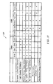
- Figure 10 depicts function 204A which could be provided by the hardware reconfigurable processor 142, functions 204 B-E to be provided by coprocessor 146, and corresponding MOPS required by each function 204. These metrics are calculated for the various pertinent signal processing datapaths.
- computationally intensive functions are further categorized according to type of operation, e.g., arithmetic/logical, control, and memory access.
- type of operation e.g., arithmetic/logical, control, and memory access.
- characteristic power per MOPS is determined for hardware or software implementation from vendor data, analysis, or other means. Power, e.g., milliwatts, required per function is thereby characterized for implementation in both reconfigurable hardware or in software (i.e., running on a processor whose power-per-MOPS has been characterized).
- the corresponding code size (and therefore memory requirement) for software implementation is determined. From the above, and from budgeted power and memory resources, allocation of processing operations to hardware and software processors can be determined.
- the entries in spreadsheet 200 correspond to static operation for a particular standard, i.e., to a specific time within a dynamic operational scenario.
- the analysis of Figure 10 must be repeated as necessary to reflect important temporal variations during representative/ realistic scenarios for all standards, applications, and/or services of interest.
- the results of these analyses must be interpreted to reveal additional critical metrics of computational intensity, including for example but not restricted to average and peak MOPS for each relevant operation. This enables the requisite specifications for the hardware and software processing resources to be further evaluated.
- the second step of profiling involves analysis of commonality of signal processing functions across the standards, applications, and/or services of interest. This is represented by example in Figure 11 . Included in abridged spreadsheet 220 are representative standards/ applications, and respective relevant signal processing functions within the general category of parameter estimation. Figure 11 shows, for example, that a Windowed Average Energy Estimator is required by seven of the listed standards. The designer would research the respective requirements of each of these seven standards to determine the required superset and seven subsets of functionality.
- each unique type of kernel includes a combination of variable and invariant functionality.
- the invariant component is determined by the above steps to be common across the standards, applications, and/or services of interest, while the variable functionality is that determined necessary to adapt to the various standards, applications, and/or services of interest.
- Each kernel is designed to include sufficient control and interface functionality to permit reconfiguration according to the end operational scenario.
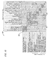
- the interconnection of kernels must also be determined from profiling as shown in the example abridged matrix 260 of Figure 13 .
- the rows and columns of matrix 260 show a representative set of hardware signal processing kernels that have been defined according to the above profiling steps, along with all connections necessary to serve a representative set of CDMA-based wireless communication standards.
- signals generally flow from bottom to top, or from right to left, with exceptions as indicated.
- Each cell containing an "X" represents a required interface between the respective kernels. It can be seen that in the vicinity of the diagonal, interconnections are tightly clustered, as for example cluster 262.
- Other types of interconnections include parallel connections, e.g., 264, and isolated connections, e.g., 266.
- connection 164 of Figure 8 connection 164 of Figure 8
- connections that must change as a function of standard etc. must be effected by the reconfigurable data router 168 of Figure 8 .
- cluster 262 indicates short connections in the silicon implementation, while cluster 266 indicates longer connections.
- Cluster 264 indicates a set of parallel connections.
- reconfiguration of multiprocessor 160 is effected by i) selection of hardware processing kernel types, ii) control of the variable kernel functionality, and iii) control of the reconfigurable data router 168.
- a kernel pool 280 includes a sufficient number of each type of kernel to permit the assembly of multiple datapaths 290.
- a sufficient multiplicity of datapaths 290 is assembled to accommodate the signal processing requirements of a particular standard, service or application. This is illustrated for a number of representative applications and/or products 300.
- the portfolio 300A-D can represent either a single product having multi-mode/standard /application capability, or multiple, separate products based on common underlying hardware and software resources.
- Initial or subsequent configuration can be performed in the factory, at point-of-sale, or by the user after delivery.
- Post-delivery customization can be based upon any of a number of techniques, including but not limited to smart card, wired interface, and over-the-air/over-the-network download and billing.
- the architecture provides the ability to reconfigure a single product platform for multiple standards, applications, services, and quality-of service, instead of developing multiple hardware platforms to establish the same collective functionality.
- the architecture also provides the ability to use software programming techniques to reduce product development time and achieve rapid and comprehensive product customization. Thus, new services can be provided via software upgrades.
- the apparatus of the invention allows a network operator or service provider to control a communication terminal's capabilities. Equipment manufacturers may exploit the invention to create software-defined communication appliances.
- the architecture of the invention optimally combines fixed-function and reconfigurable logic resources.
- the system has reconfigurable control and data paths.
- the invention extends the performance efficiency of microprocessors and digital signal processors via the augmentation of data paths and control paths through a reconfigurable co-processing machine.
- the reconfigurability of the data path optimizes the performance of the data flow in the algorithms implemented on the processor.
- the architecture efficiently redirects functions previously running on a Fixed Function Data Arithmetic Logic Unit to a more flexible Heterogeneous Reconfigurable Multiprocessing Unit.
- the invention does not depend upon the fine-grained reconfigurability of existing programmable logic devices, and so does not have the problem of such devices of the area and power of the chip being dominated by the routing resources. Furthermore, the invention does not substantially rely on instruction-set programmable processors. Instead, a quasi-fixed set of computational resources that span the signal processing requirements of the standards, applications, and/or services of interest are configured together in a reprogrammable manner.
- This architecture can be applied to implement signal processing and/or control of processing applications. Ideal applications include but are not limited to digital communication, networking, encryption/security, and multimedia applications.
- the invention reduces product development time via the use of a reconfigurable processor that is programmable via a high-level language. This avoids the problem of having to create new processors each time the algorithms considered for new applications change or push the performance envelope of existing processor architectures.
- the invention enables mass customization of relevant consumer and infrastructure products.
Landscapes
- Engineering & Computer Science (AREA)
- Computer Networks & Wireless Communication (AREA)
- Signal Processing (AREA)
- Mobile Radio Communication Systems (AREA)
- Transceivers (AREA)
- Communication Control (AREA)
Claims (7)
- Eine digitale Drahtloskommunikationsvorrichtung, die folgende Merkmale aufweist:ein Hochfrequenzuntersystem (26) (HF-Untersystem);einen Analog-zu-Digital-Wandler (28);einen softwareprogrammierbaren Prozessor (72, 74), wobei der softwareprogrammierbare Prozessor (72, 74) einen Digitalsignalprozessor (72) oder eine zentrale Verarbeitungseinheit (74) aufweist und wobei der softwareprogrammierbare Prozessor (72, 74) einen Satz von Softwaremodulen ausführt, die einen Satz von Drahtloskommunikationsanwendungen, -Standards oder -Diensten spezifizieren, die implementiert werden sollen;eine heterogene rekonfigurierbare Mehrfachverarbeitungslogikschaltung (66, 142, 146, 160), wobei die heterogene rekonfigurierbare Mehrfachverarbeitungslogikschaltung (66, 142, 146, 160) eine Mehrzahl von programmierbaren Datenverarbeitungskernen (162, 162A, 162B, 162C) aufweist, wobei Verbindungen (164) zwischen den Datenverarbeitungskernen (162A, 162B) direkt hergestellt sind, wobei die Verbindungen (164) über alle interessierenden Standards, Anwendungen und/oder Dienste üblich sind, wobei Verbindungen (166A - 166F, 172A - 172D) zwischen den programmierbaren Datenverarbeitungskernen (162A, 162B), die sich in Abhängigkeit von interessierenden Standards, Anwendungen und/oder Diensten verändern müssen, durch einen rekonfigurierbaren Datenrouter (168) bewirkt sind, wobei die Mehrzahl von programmierbaren Datenverarbeitungskernen (162, 162A, 162B, 162C) programmiert ist, um einen Satz von Drahtloskommunikationsanwendungen, -Standards oder -Diensten zu implementieren, und wobei die Mehrzahl von programmierbaren Datenverarbeitungskernen (162, 162A, 162B, 162C) und der rekonfigurierbare Datenrouter (168) durch den softwareprogrammierbaren Prozessor (72, 74) gesteuert sind; undeinen Bus (52, 55), der den softwareprogrammierbaren Prozessor (72, 74) und die heterogene rekonfigurierbare Mehrfachverarbeitungslogikschaltung (66, 142, 146, 160) verbindet.
- Die digitale Drahtloskommunikationsvorrichtung gemäß Anspruch 1, bei der jeder Datenverarbeitungskern (162, 162A, 162B, 162C) der Mehrzahl von Datenverarbeitungskernen (162, 162A, 162B, 162C) einen Datensequenzierer (184), einen lokalen Speicher (182) und eine Arithmetik-Logik-Einheit (186) umfasst.
- Ein Verfahren zum Programmieren einer digitalen Drahtloskommunikationsvorrichtung (100, 140) gemäß einem der Ansprüche 1 bis 2, um eine Drahtloskommunikationsanwendung, einen -Standard und einen -Dienst zu unterstützen, wobei das Verfahren folgende Schritte aufweist:Auswählen eines Satzes von Parametern und Werten, die erforderlich sind, um eine spezifizierte Drahtloskommunikationsanwendung, einen -Standard und einen -Dienst zu implementieren;Herunterladen des Satzes von Parametern und Werten zu einer digitalen Drahtloskommunikationsvorrichtung (100, 140), die eine heterogene rekonfigurierbare Mehrfachverarbeitungslogikschaltung (66, 142, 146, 160) mit einer Mehrzahl von reprogrammierbaren Datenverarbeitungskernen (162, 162A, 162B, 162C) umfasst; undBetreiben der Mehrzahl von reprogrammierbaren Datenverarbeitungskernen (162, 162A, 162B, 162C) gemäß dem Satz von Parametern und Werten, um die spezifizierte Kommunikationsanwendung, den -Standard und den -Dienst zu unterstützen.
- Das Verfahren gemäß Anspruch 3, bei dem der Auswahlschritt den Schritt eines Auswählens eines Satzes von Parametern und Werten aus der Gruppe umfasst, die Folgendes aufweist: ein Betriebsland, ein Frequenzband und eine Datenrate.
- Das Verfahren gemäß Anspruch 3, bei dem der Herunterladeschritt den Schritt eines Herunterladens des Satzes von Parametern über einen Drahtloskommunikationskanal umfasst.
- Das Verfahren gemäß Anspruch 3, bei dem der Herunterladeschritt den Schritt eines Herunterladens des Satzes von Parametern zu der Herstellungszeit umfasst.
- Das Verfahren gemäß Anspruch 3, bei dem der Herunterladeschritt den Schritt eines Herunterladens des Satzes von Parametern an einer Verkaufsstelle umfasst.
Priority Applications (1)
| Application Number | Priority Date | Filing Date | Title |
|---|---|---|---|
| EP06016938A EP1746736A3 (de) | 1999-05-07 | 2000-05-05 | Betriebsverfahren und reprogrammierbare digitale drahtlose Vorrichtung |
Applications Claiming Priority (9)
| Application Number | Priority Date | Filing Date | Title |
|---|---|---|---|
| US13312999P | 1999-05-07 | 1999-05-07 | |
| US13313799P | 1999-05-07 | 1999-05-07 | |
| US13313599P | 1999-05-07 | 1999-05-07 | |
| US13314199P | 1999-05-07 | 1999-05-07 | |
| US133141P | 1999-05-07 | ||
| US133135P | 1999-05-07 | ||
| US133137P | 1999-05-07 | ||
| US133129P | 1999-05-07 | ||
| PCT/US2000/012473 WO2000069084A1 (en) | 1999-05-07 | 2000-05-05 | Reprogrammable digital wireless communication device and method of operating same |
Related Child Applications (1)
| Application Number | Title | Priority Date | Filing Date |
|---|---|---|---|
| EP06016938A Division EP1746736A3 (de) | 1999-05-07 | 2000-05-05 | Betriebsverfahren und reprogrammierbare digitale drahtlose Vorrichtung |
Publications (3)
| Publication Number | Publication Date |
|---|---|
| EP1188246A1 EP1188246A1 (de) | 2002-03-20 |
| EP1188246A4 EP1188246A4 (de) | 2005-08-03 |
| EP1188246B1 true EP1188246B1 (de) | 2009-03-11 |
Family
ID=27495012
Family Applications (1)
| Application Number | Title | Priority Date | Filing Date |
|---|---|---|---|
| EP00935875A Expired - Lifetime EP1188246B1 (de) | 1999-05-07 | 2000-05-05 | Reprogrammierbare digitale drahtlose Vorrichtung und Verfahren zur Nutzung derselben |
Country Status (8)
| Country | Link |
|---|---|
| EP (1) | EP1188246B1 (de) |
| JP (1) | JP4518675B2 (de) |
| KR (1) | KR100748394B1 (de) |
| AT (1) | ATE425590T1 (de) |
| AU (1) | AU5127100A (de) |
| CA (1) | CA2371084A1 (de) |
| DE (1) | DE60041766D1 (de) |
| WO (1) | WO2000069084A1 (de) |
Families Citing this family (19)
| Publication number | Priority date | Publication date | Assignee | Title |
|---|---|---|---|---|
| US7085285B2 (en) | 2000-03-01 | 2006-08-01 | Realtek Semiconductor Corp. | xDSL communications systems using shared/multi-function task blocks |
| AU2001286410A1 (en) | 2000-07-31 | 2002-02-13 | Morphics Technology, Inc. | Method and apparatus for time-sliced and multi-threaded data processing in a communication system |
| US7151925B2 (en) | 2001-09-10 | 2006-12-19 | Industrial Technology Research Institute | Software defined radio (SDR) architecture for wireless digital communication systems |
| EP1440519B1 (de) | 2001-10-31 | 2006-08-02 | Infineon Technologies AG | Hardware-Struktur und Verfahren für eine Sende-Empfangseinrichtung mit konfigurierbaren Coprozessor für Mobilfunkanwendungen |
| US8079015B2 (en) | 2002-02-15 | 2011-12-13 | Telefonaktiebolaget L M Ericsson (Publ) | Layered architecture for mobile terminals |
| US7415270B2 (en) | 2002-02-15 | 2008-08-19 | Telefonaktiebolaget L M Ericsson (Publ) | Middleware services layer for platform system for mobile terminals |
| US7536181B2 (en) | 2002-02-15 | 2009-05-19 | Telefonaktiebolaget L M Ericsson (Publ) | Platform system for mobile terminals |
| US7363033B2 (en) | 2002-02-15 | 2008-04-22 | Telefonaktiebolaget Lm Ericsson (Publ) | Method of and system for testing equipment during manufacturing |
| US7149510B2 (en) | 2002-09-23 | 2006-12-12 | Telefonaktiebolaget Lm Ericsson (Publ) | Security access manager in middleware |
| AU2003277881A1 (en) * | 2002-09-23 | 2004-04-08 | Telefonaktiebolaget Lm Ericsson (Publ) | Middleware application message/event model |
| US7584471B2 (en) | 2002-09-23 | 2009-09-01 | Telefonaktiebolaget L M Ericsson (Publ) | Plug-in model |
| US7350211B2 (en) | 2002-09-23 | 2008-03-25 | Telefonaktiebolaget Lm Ericsson (Publ) | Middleware application environment |
| TWI234714B (en) | 2003-12-03 | 2005-06-21 | Ind Tech Res Inst | Reconfigurable radio processor architecture |
| JP4475145B2 (ja) | 2005-03-04 | 2010-06-09 | 株式会社日立製作所 | ソフトウェア無線機及びライブラリ構成 |
| KR100696944B1 (ko) * | 2005-03-30 | 2007-03-20 | 전자부품연구원 | 하이브리드 소프트웨어-정의 라디오 |
| JP2007266916A (ja) * | 2006-03-28 | 2007-10-11 | Mitsubishi Electric Corp | データリンク装置 |
| EP2256937B1 (de) * | 2009-05-28 | 2011-12-28 | Universität Duisburg-Essen | Digitaler Empfänger, digitaler Sender, Verfahren zur Bedienung eines digitalen Empfängers oder eines digitalen Senders und Computerprogramm |
| DE102010056080A1 (de) * | 2010-12-23 | 2012-06-28 | Hydrometer Electronic Gmbh | Funkempfänger und Verfahren zu seinem Betrieb |
| CN111478799B (zh) * | 2020-03-19 | 2022-11-29 | 中国电子产品可靠性与环境试验研究所((工业和信息化部电子第五研究所)(中国赛宝实验室)) | 一种基于动态重构的异构工业网络互联方法及无线模块 |
Family Cites Families (6)
| Publication number | Priority date | Publication date | Assignee | Title |
|---|---|---|---|---|
| US5539479A (en) * | 1995-05-31 | 1996-07-23 | International Business Machines Corporation | Video receiver display of cursor and menu overlaying video |
| US5872810A (en) * | 1996-01-26 | 1999-02-16 | Imec Co. | Programmable modem apparatus for transmitting and receiving digital data, design method and use method for said modem |
| US5907580A (en) * | 1996-06-10 | 1999-05-25 | Morphics Technology, Inc | Method and apparatus for communicating information |
| JPH1078932A (ja) * | 1996-09-04 | 1998-03-24 | Hitachi Ltd | リコンフィグラブル・ネットワークコンピュータ |
| JP3842394B2 (ja) * | 1997-08-06 | 2006-11-08 | 株式会社ケンウッド | 無線機 |
| US6185418B1 (en) * | 1997-11-07 | 2001-02-06 | Lucent Technologies Inc. | Adaptive digital radio communication system |
-
2000
- 2000-05-05 AT AT00935875T patent/ATE425590T1/de not_active IP Right Cessation
- 2000-05-05 CA CA002371084A patent/CA2371084A1/en not_active Abandoned
- 2000-05-05 KR KR1020017014231A patent/KR100748394B1/ko not_active Expired - Fee Related
- 2000-05-05 JP JP2000617569A patent/JP4518675B2/ja not_active Expired - Fee Related
- 2000-05-05 EP EP00935875A patent/EP1188246B1/de not_active Expired - Lifetime
- 2000-05-05 DE DE60041766T patent/DE60041766D1/de not_active Expired - Lifetime
- 2000-05-05 WO PCT/US2000/012473 patent/WO2000069084A1/en not_active Ceased
- 2000-05-05 AU AU51271/00A patent/AU5127100A/en not_active Abandoned
Also Published As
| Publication number | Publication date |
|---|---|
| JP4518675B2 (ja) | 2010-08-04 |
| JP2002544704A (ja) | 2002-12-24 |
| EP1188246A4 (de) | 2005-08-03 |
| EP1188246A1 (de) | 2002-03-20 |
| ATE425590T1 (de) | 2009-03-15 |
| DE60041766D1 (de) | 2009-04-23 |
| KR100748394B1 (ko) | 2007-08-10 |
| CA2371084A1 (en) | 2000-11-16 |
| WO2000069084A9 (en) | 2002-08-29 |
| KR20020072492A (ko) | 2002-09-16 |
| WO2000069084A1 (en) | 2000-11-16 |
| AU5127100A (en) | 2000-11-21 |
Similar Documents
| Publication | Publication Date | Title |
|---|---|---|
| US6721581B1 (en) | Reprogrammable digital wireless communication device and method of operating same | |
| EP1188246B1 (de) | Reprogrammierbare digitale drahtlose Vorrichtung und Verfahren zur Nutzung derselben | |
| US6967999B2 (en) | Method and apparatus to support multi standard, multi service base-stations for wireless voice and data networks | |
| US7188159B2 (en) | Efficient software download to configurable communication device | |
| CN101031901B (zh) | 用于不同通信标准的同步实现的低功率可重构体系 | |
| KR100347658B1 (ko) | 정보를전달하기위한방법및장치 | |
| US20030050055A1 (en) | Software defined radio (SDR) architecture for wireless digital communication systems | |
| Srikanteswara et al. | A soft radio architecture for reconfigurable platforms | |
| US8225073B2 (en) | Apparatus, system and method for configuration of adaptive integrated circuitry having heterogeneous computational elements | |
| US8504661B2 (en) | Apparatus and method for adaptive multimedia reception and transmission in communication environments | |
| MITOLA III | Software radio architecture evolution: Foundations, technology tradeoffs, and architecture implications | |
| US20060031660A1 (en) | Apparatus, method, system and executable module for configuration and operation of adaptive integrated circuitry having fixed, application specific computational elements | |
| US20020059481A1 (en) | Method and apparatus for a multimedia application specific processor | |
| EP1746736A2 (de) | Betriebsverfahren und reprogrammierbare digitale drahtlose Vorrichtung | |
| WO2004047387A2 (en) | Packet based reconfigurable system architecture | |
| Marylin et al. | Software radio: the challenges for reconfigurable terminals | |
| Srikanteswara et al. | Soft radio implementations for 3G and future high data rate systems | |
| Said | PicoRF: A PC-based SDR platform using a high performance PCIe plug-in card extension | |
| Al-Adnani | Multimode reconfigurable software defined radio | |
| Bronzel et al. | Functional Elements in E2E Reconfigurable Equipment |
Legal Events
| Date | Code | Title | Description |
|---|---|---|---|
| PUAI | Public reference made under article 153(3) epc to a published international application that has entered the european phase |
Free format text: ORIGINAL CODE: 0009012 |
|
| 17P | Request for examination filed |
Effective date: 20011122 |
|
| AK | Designated contracting states |
Kind code of ref document: A1 Designated state(s): AT BE CH CY DE DK ES FI FR GB GR IE IT LI LU MC NL PT SE |
|
| AX | Request for extension of the european patent |
Free format text: AL;LT;LV;MK;RO;SI |
|
| RAP1 | Party data changed (applicant data changed or rights of an application transferred) |
Owner name: INFINEON TECHNOLOGIES AG |
|
| A4 | Supplementary search report drawn up and despatched |
Effective date: 20050621 |
|
| 17Q | First examination report despatched |
Effective date: 20060206 |
|
| GRAP | Despatch of communication of intention to grant a patent |
Free format text: ORIGINAL CODE: EPIDOSNIGR1 |
|
| RTI1 | Title (correction) |
Free format text: REPROGRAMMABLE DIGITAL WIRELESS COMMUNICATION DEVICE AND METHOD OF OPERATING SAME |
|
| GRAS | Grant fee paid |
Free format text: ORIGINAL CODE: EPIDOSNIGR3 |
|
| GRAA | (expected) grant |
Free format text: ORIGINAL CODE: 0009210 |
|
| AK | Designated contracting states |
Kind code of ref document: B1 Designated state(s): AT BE CH CY DE DK ES FI FR GB GR IE IT LI LU MC NL PT SE |
|
| REG | Reference to a national code |
Ref country code: GB Ref legal event code: FG4D |
|
| REG | Reference to a national code |
Ref country code: CH Ref legal event code: EP |
|
| REG | Reference to a national code |
Ref country code: IE Ref legal event code: FG4D |
|
| REF | Corresponds to: |
Ref document number: 60041766 Country of ref document: DE Date of ref document: 20090423 Kind code of ref document: P |
|
| PG25 | Lapsed in a contracting state [announced via postgrant information from national office to epo] |
Ref country code: NL Free format text: LAPSE BECAUSE OF FAILURE TO SUBMIT A TRANSLATION OF THE DESCRIPTION OR TO PAY THE FEE WITHIN THE PRESCRIBED TIME-LIMIT Effective date: 20090311 Ref country code: FI Free format text: LAPSE BECAUSE OF FAILURE TO SUBMIT A TRANSLATION OF THE DESCRIPTION OR TO PAY THE FEE WITHIN THE PRESCRIBED TIME-LIMIT Effective date: 20090311 |
|
| NLV1 | Nl: lapsed or annulled due to failure to fulfill the requirements of art. 29p and 29m of the patents act | ||
| PG25 | Lapsed in a contracting state [announced via postgrant information from national office to epo] |
Ref country code: AT Free format text: LAPSE BECAUSE OF FAILURE TO SUBMIT A TRANSLATION OF THE DESCRIPTION OR TO PAY THE FEE WITHIN THE PRESCRIBED TIME-LIMIT Effective date: 20090311 Ref country code: SE Free format text: LAPSE BECAUSE OF FAILURE TO SUBMIT A TRANSLATION OF THE DESCRIPTION OR TO PAY THE FEE WITHIN THE PRESCRIBED TIME-LIMIT Effective date: 20090611 |
|
| PG25 | Lapsed in a contracting state [announced via postgrant information from national office to epo] |
Ref country code: BE Free format text: LAPSE BECAUSE OF FAILURE TO SUBMIT A TRANSLATION OF THE DESCRIPTION OR TO PAY THE FEE WITHIN THE PRESCRIBED TIME-LIMIT Effective date: 20090311 |
|
| PG25 | Lapsed in a contracting state [announced via postgrant information from national office to epo] |
Ref country code: PT Free format text: LAPSE BECAUSE OF FAILURE TO SUBMIT A TRANSLATION OF THE DESCRIPTION OR TO PAY THE FEE WITHIN THE PRESCRIBED TIME-LIMIT Effective date: 20090824 Ref country code: ES Free format text: LAPSE BECAUSE OF FAILURE TO SUBMIT A TRANSLATION OF THE DESCRIPTION OR TO PAY THE FEE WITHIN THE PRESCRIBED TIME-LIMIT Effective date: 20090622 |
|
| PG25 | Lapsed in a contracting state [announced via postgrant information from national office to epo] |
Ref country code: MC Free format text: LAPSE BECAUSE OF NON-PAYMENT OF DUE FEES Effective date: 20090531 |
|
| REG | Reference to a national code |
Ref country code: CH Ref legal event code: PL |
|
| PLBE | No opposition filed within time limit |
Free format text: ORIGINAL CODE: 0009261 |
|
| STAA | Information on the status of an ep patent application or granted ep patent |
Free format text: STATUS: NO OPPOSITION FILED WITHIN TIME LIMIT |
|
| PG25 | Lapsed in a contracting state [announced via postgrant information from national office to epo] |
Ref country code: DK Free format text: LAPSE BECAUSE OF FAILURE TO SUBMIT A TRANSLATION OF THE DESCRIPTION OR TO PAY THE FEE WITHIN THE PRESCRIBED TIME-LIMIT Effective date: 20090311 Ref country code: CH Free format text: LAPSE BECAUSE OF NON-PAYMENT OF DUE FEES Effective date: 20090531 Ref country code: LI Free format text: LAPSE BECAUSE OF NON-PAYMENT OF DUE FEES Effective date: 20090531 |
|
| 26N | No opposition filed |
Effective date: 20091214 |
|
| PG25 | Lapsed in a contracting state [announced via postgrant information from national office to epo] |
Ref country code: IE Free format text: LAPSE BECAUSE OF NON-PAYMENT OF DUE FEES Effective date: 20090505 |
|
| PG25 | Lapsed in a contracting state [announced via postgrant information from national office to epo] |
Ref country code: GR Free format text: LAPSE BECAUSE OF FAILURE TO SUBMIT A TRANSLATION OF THE DESCRIPTION OR TO PAY THE FEE WITHIN THE PRESCRIBED TIME-LIMIT Effective date: 20090612 |
|
| PG25 | Lapsed in a contracting state [announced via postgrant information from national office to epo] |
Ref country code: IT Free format text: LAPSE BECAUSE OF FAILURE TO SUBMIT A TRANSLATION OF THE DESCRIPTION OR TO PAY THE FEE WITHIN THE PRESCRIBED TIME-LIMIT Effective date: 20090311 |
|
| PG25 | Lapsed in a contracting state [announced via postgrant information from national office to epo] |
Ref country code: LU Free format text: LAPSE BECAUSE OF NON-PAYMENT OF DUE FEES Effective date: 20090505 |
|
| PG25 | Lapsed in a contracting state [announced via postgrant information from national office to epo] |
Ref country code: CY Free format text: LAPSE BECAUSE OF FAILURE TO SUBMIT A TRANSLATION OF THE DESCRIPTION OR TO PAY THE FEE WITHIN THE PRESCRIBED TIME-LIMIT Effective date: 20090311 |
|
| REG | Reference to a national code |
Ref country code: FR Ref legal event code: TP Owner name: INTEL MOBILE COMMUNICATIONS GMBH, DE Effective date: 20120404 Ref country code: FR Ref legal event code: CA Effective date: 20120404 |
|
| REG | Reference to a national code |
Ref country code: GB Ref legal event code: 732E Free format text: REGISTERED BETWEEN 20120607 AND 20120613 |
|
| REG | Reference to a national code |
Ref country code: GB Ref legal event code: 732E Free format text: REGISTERED BETWEEN 20121213 AND 20121219 |
|
| REG | Reference to a national code |
Ref country code: DE Ref legal event code: R081 Ref document number: 60041766 Country of ref document: DE Owner name: INTEL MOBILE COMMUNICATIONS GMBH, DE Free format text: FORMER OWNER: INTEL MOBILE COMMUNICATIONS GMBH, 85579 NEUBIBERG, DE Effective date: 20130315 Ref country code: DE Ref legal event code: R081 Ref document number: 60041766 Country of ref document: DE Owner name: INTEL MOBILE COMMUNICATIONS GMBH, DE Free format text: FORMER OWNER: INFINEON TECHNOLOGIES AG, 85579 NEUBIBERG, DE Effective date: 20130315 Ref country code: DE Ref legal event code: R081 Ref document number: 60041766 Country of ref document: DE Owner name: INTEL MOBILE COMMUNICATIONS GMBH, DE Free format text: FORMER OWNER: INTEL MOBILE COMMUNICATIONS TECHNOLOGY GMBH, 85579 NEUBIBERG, DE Effective date: 20130326 Ref country code: DE Ref legal event code: R081 Ref document number: 60041766 Country of ref document: DE Owner name: INTEL MOBILE COMMUNICATIONS GMBH, DE Free format text: FORMER OWNER: INFINEON TECHNOLOGIES AG, 85579 NEUBIBERG, DE Effective date: 20130314 Ref country code: DE Ref legal event code: R081 Ref document number: 60041766 Country of ref document: DE Owner name: INTEL DEUTSCHLAND GMBH, DE Free format text: FORMER OWNER: INFINEON TECHNOLOGIES AG, 85579 NEUBIBERG, DE Effective date: 20130315 Ref country code: DE Ref legal event code: R081 Ref document number: 60041766 Country of ref document: DE Owner name: INTEL DEUTSCHLAND GMBH, DE Free format text: FORMER OWNER: INTEL MOBILE COMMUNICATIONS TECHNOLOGY GMBH, 85579 NEUBIBERG, DE Effective date: 20130326 Ref country code: DE Ref legal event code: R081 Ref document number: 60041766 Country of ref document: DE Owner name: INTEL DEUTSCHLAND GMBH, DE Free format text: FORMER OWNER: INTEL MOBILE COMMUNICATIONS GMBH, 85579 NEUBIBERG, DE Effective date: 20130315 Ref country code: DE Ref legal event code: R081 Ref document number: 60041766 Country of ref document: DE Owner name: INTEL DEUTSCHLAND GMBH, DE Free format text: FORMER OWNER: INFINEON TECHNOLOGIES AG, 85579 NEUBIBERG, DE Effective date: 20130314 |
|
| REG | Reference to a national code |
Ref country code: FR Ref legal event code: PLFP Year of fee payment: 16 |
|
| REG | Reference to a national code |
Ref country code: DE Ref legal event code: R081 Ref document number: 60041766 Country of ref document: DE Owner name: INTEL DEUTSCHLAND GMBH, DE Free format text: FORMER OWNER: INTEL MOBILE COMMUNICATIONS GMBH, 85579 NEUBIBERG, DE |
|
| REG | Reference to a national code |
Ref country code: FR Ref legal event code: CD Owner name: INTEL DEUTSCHLAND GMBH, DE Effective date: 20160126 |
|
| REG | Reference to a national code |
Ref country code: FR Ref legal event code: PLFP Year of fee payment: 17 |
|
| PGFP | Annual fee paid to national office [announced via postgrant information from national office to epo] |
Ref country code: GB Payment date: 20160504 Year of fee payment: 17 |
|
| PGFP | Annual fee paid to national office [announced via postgrant information from national office to epo] |
Ref country code: FR Payment date: 20160426 Year of fee payment: 17 |
|
| GBPC | Gb: european patent ceased through non-payment of renewal fee |
Effective date: 20170505 |
|
| REG | Reference to a national code |
Ref country code: FR Ref legal event code: ST Effective date: 20180131 |
|
| PG25 | Lapsed in a contracting state [announced via postgrant information from national office to epo] |
Ref country code: GB Free format text: LAPSE BECAUSE OF NON-PAYMENT OF DUE FEES Effective date: 20170505 |
|
| PG25 | Lapsed in a contracting state [announced via postgrant information from national office to epo] |
Ref country code: FR Free format text: LAPSE BECAUSE OF NON-PAYMENT OF DUE FEES Effective date: 20170531 |
|
| PGFP | Annual fee paid to national office [announced via postgrant information from national office to epo] |
Ref country code: DE Payment date: 20190423 Year of fee payment: 20 |
|
| REG | Reference to a national code |
Ref country code: DE Ref legal event code: R071 Ref document number: 60041766 Country of ref document: DE |