EP1189087A2 - Récepteur photonique monolithique comprenant un support de fibre autoaligné adapté pour assemblage du type flip chip - Google Patents
Récepteur photonique monolithique comprenant un support de fibre autoaligné adapté pour assemblage du type flip chip Download PDFInfo
- Publication number
- EP1189087A2 EP1189087A2 EP20010117690 EP01117690A EP1189087A2 EP 1189087 A2 EP1189087 A2 EP 1189087A2 EP 20010117690 EP20010117690 EP 20010117690 EP 01117690 A EP01117690 A EP 01117690A EP 1189087 A2 EP1189087 A2 EP 1189087A2
- Authority
- EP
- European Patent Office
- Prior art keywords
- chip
- front side
- crystal plane
- reflective mirror
- channel
- Prior art date
- Legal status (The legal status is an assumption and is not a legal conclusion. Google has not performed a legal analysis and makes no representation as to the accuracy of the status listed.)
- Withdrawn
Links
- 239000000835 fiber Substances 0.000 title description 29
- 239000013078 crystal Substances 0.000 claims abstract description 45
- 230000003287 optical effect Effects 0.000 claims abstract description 35
- 230000005693 optoelectronics Effects 0.000 claims abstract description 27
- 238000000034 method Methods 0.000 claims description 52
- 239000000463 material Substances 0.000 claims description 26
- 229920002120 photoresistant polymer Polymers 0.000 claims description 24
- 238000005530 etching Methods 0.000 claims description 16
- 238000004519 manufacturing process Methods 0.000 claims description 12
- 239000004065 semiconductor Substances 0.000 claims description 9
- GPXJNWSHGFTCBW-UHFFFAOYSA-N Indium phosphide Chemical compound [In]#P GPXJNWSHGFTCBW-UHFFFAOYSA-N 0.000 claims description 5
- 239000011248 coating agent Substances 0.000 claims description 5
- 238000000576 coating method Methods 0.000 claims description 5
- JBRZTFJDHDCESZ-UHFFFAOYSA-N AsGa Chemical compound [As]#[Ga] JBRZTFJDHDCESZ-UHFFFAOYSA-N 0.000 claims description 4
- HZXMRANICFIONG-UHFFFAOYSA-N gallium phosphide Chemical compound [Ga]#P HZXMRANICFIONG-UHFFFAOYSA-N 0.000 claims description 4
- RPQDHPTXJYYUPQ-UHFFFAOYSA-N indium arsenide Chemical compound [In]#[As] RPQDHPTXJYYUPQ-UHFFFAOYSA-N 0.000 claims description 4
- 239000007769 metal material Substances 0.000 claims description 2
- 238000010168 coupling process Methods 0.000 abstract description 10
- 230000008878 coupling Effects 0.000 abstract description 9
- 238000005859 coupling reaction Methods 0.000 abstract description 9
- 230000008569 process Effects 0.000 description 21
- CSCPPACGZOOCGX-UHFFFAOYSA-N Acetone Chemical compound CC(C)=O CSCPPACGZOOCGX-UHFFFAOYSA-N 0.000 description 16
- 239000010931 gold Substances 0.000 description 16
- XLYOFNOQVPJJNP-UHFFFAOYSA-N water Chemical compound O XLYOFNOQVPJJNP-UHFFFAOYSA-N 0.000 description 16
- 239000008367 deionised water Substances 0.000 description 15
- 229910021641 deionized water Inorganic materials 0.000 description 15
- 239000013307 optical fiber Substances 0.000 description 15
- KFZMGEQAYNKOFK-UHFFFAOYSA-N Isopropanol Chemical compound CC(C)O KFZMGEQAYNKOFK-UHFFFAOYSA-N 0.000 description 12
- 239000000758 substrate Substances 0.000 description 9
- 239000010408 film Substances 0.000 description 7
- 229910052751 metal Inorganic materials 0.000 description 7
- 239000002184 metal Substances 0.000 description 7
- 238000000206 photolithography Methods 0.000 description 7
- NBIIXXVUZAFLBC-UHFFFAOYSA-N Phosphoric acid Chemical compound OP(O)(O)=O NBIIXXVUZAFLBC-UHFFFAOYSA-N 0.000 description 6
- VYPSYNLAJGMNEJ-UHFFFAOYSA-N Silicium dioxide Chemical compound O=[Si]=O VYPSYNLAJGMNEJ-UHFFFAOYSA-N 0.000 description 6
- 238000007906 compression Methods 0.000 description 5
- 238000000151 deposition Methods 0.000 description 5
- 229910052737 gold Inorganic materials 0.000 description 5
- 238000002161 passivation Methods 0.000 description 5
- 229910000679 solder Inorganic materials 0.000 description 5
- KWYUFKZDYYNOTN-UHFFFAOYSA-M Potassium hydroxide Chemical compound [OH-].[K+] KWYUFKZDYYNOTN-UHFFFAOYSA-M 0.000 description 4
- 229910052581 Si3N4 Inorganic materials 0.000 description 4
- QAOWNCQODCNURD-UHFFFAOYSA-N Sulfuric acid Chemical compound OS(O)(=O)=O QAOWNCQODCNURD-UHFFFAOYSA-N 0.000 description 4
- 229910052782 aluminium Inorganic materials 0.000 description 4
- PCHJSUWPFVWCPO-UHFFFAOYSA-N gold Chemical compound [Au] PCHJSUWPFVWCPO-UHFFFAOYSA-N 0.000 description 4
- 150000002736 metal compounds Chemical class 0.000 description 4
- 238000001465 metallisation Methods 0.000 description 4
- 239000004033 plastic Substances 0.000 description 4
- HQVNEWCFYHHQES-UHFFFAOYSA-N silicon nitride Chemical compound N12[Si]34N5[Si]62N3[Si]51N64 HQVNEWCFYHHQES-UHFFFAOYSA-N 0.000 description 4
- 239000010409 thin film Substances 0.000 description 4
- MHAJPDPJQMAIIY-UHFFFAOYSA-N Hydrogen peroxide Chemical compound OO MHAJPDPJQMAIIY-UHFFFAOYSA-N 0.000 description 3
- XAGFODPZIPBFFR-UHFFFAOYSA-N aluminium Chemical compound [Al] XAGFODPZIPBFFR-UHFFFAOYSA-N 0.000 description 3
- 238000005229 chemical vapour deposition Methods 0.000 description 3
- 238000004140 cleaning Methods 0.000 description 3
- 230000000295 complement effect Effects 0.000 description 3
- 239000003989 dielectric material Substances 0.000 description 3
- 230000005496 eutectics Effects 0.000 description 3
- 229910052738 indium Inorganic materials 0.000 description 3
- APFVFJFRJDLVQX-UHFFFAOYSA-N indium atom Chemical compound [In] APFVFJFRJDLVQX-UHFFFAOYSA-N 0.000 description 3
- 230000010354 integration Effects 0.000 description 3
- 239000000203 mixture Substances 0.000 description 3
- 238000001020 plasma etching Methods 0.000 description 3
- 239000000377 silicon dioxide Substances 0.000 description 3
- 235000012239 silicon dioxide Nutrition 0.000 description 3
- 229910001868 water Inorganic materials 0.000 description 3
- XSTXAVWGXDQKEL-UHFFFAOYSA-N Trichloroethylene Chemical compound ClC=C(Cl)Cl XSTXAVWGXDQKEL-UHFFFAOYSA-N 0.000 description 2
- 229910000147 aluminium phosphate Inorganic materials 0.000 description 2
- 238000000429 assembly Methods 0.000 description 2
- 230000000712 assembly Effects 0.000 description 2
- 230000005540 biological transmission Effects 0.000 description 2
- 230000015572 biosynthetic process Effects 0.000 description 2
- 230000006835 compression Effects 0.000 description 2
- 230000003247 decreasing effect Effects 0.000 description 2
- 230000008021 deposition Effects 0.000 description 2
- 230000009977 dual effect Effects 0.000 description 2
- 238000010894 electron beam technology Methods 0.000 description 2
- 239000007789 gas Substances 0.000 description 2
- JVPLOXQKFGYFMN-UHFFFAOYSA-N gold tin Chemical compound [Sn].[Au] JVPLOXQKFGYFMN-UHFFFAOYSA-N 0.000 description 2
- 239000012535 impurity Substances 0.000 description 2
- 238000010137 moulding (plastic) Methods 0.000 description 2
- -1 polypropylene Polymers 0.000 description 2
- 238000012545 processing Methods 0.000 description 2
- 238000004544 sputter deposition Methods 0.000 description 2
- KDYFGRWQOYBRFD-UHFFFAOYSA-N succinic acid Chemical compound OC(=O)CCC(O)=O KDYFGRWQOYBRFD-UHFFFAOYSA-N 0.000 description 2
- TXEYQDLBPFQVAA-UHFFFAOYSA-N tetrafluoromethane Chemical compound FC(F)(F)F TXEYQDLBPFQVAA-UHFFFAOYSA-N 0.000 description 2
- VOPWNXZWBYDODV-UHFFFAOYSA-N Chlorodifluoromethane Chemical compound FC(F)Cl VOPWNXZWBYDODV-UHFFFAOYSA-N 0.000 description 1
- 239000004593 Epoxy Substances 0.000 description 1
- GYHNNYVSQQEPJS-UHFFFAOYSA-N Gallium Chemical compound [Ga] GYHNNYVSQQEPJS-UHFFFAOYSA-N 0.000 description 1
- XEEYBQQBJWHFJM-UHFFFAOYSA-N Iron Chemical compound [Fe] XEEYBQQBJWHFJM-UHFFFAOYSA-N 0.000 description 1
- 239000004642 Polyimide Substances 0.000 description 1
- 239000004743 Polypropylene Substances 0.000 description 1
- 239000002253 acid Substances 0.000 description 1
- 238000013459 approach Methods 0.000 description 1
- 238000003491 array Methods 0.000 description 1
- QVGXLLKOCUKJST-UHFFFAOYSA-N atomic oxygen Chemical compound [O] QVGXLLKOCUKJST-UHFFFAOYSA-N 0.000 description 1
- MVPPADPHJFYWMZ-UHFFFAOYSA-N chlorobenzene Chemical compound ClC1=CC=CC=C1 MVPPADPHJFYWMZ-UHFFFAOYSA-N 0.000 description 1
- KRVSOGSZCMJSLX-UHFFFAOYSA-L chromic acid Substances O[Cr](O)(=O)=O KRVSOGSZCMJSLX-UHFFFAOYSA-L 0.000 description 1
- 229910017052 cobalt Inorganic materials 0.000 description 1
- 239000010941 cobalt Substances 0.000 description 1
- GUTLYIVDDKVIGB-UHFFFAOYSA-N cobalt atom Chemical compound [Co] GUTLYIVDDKVIGB-UHFFFAOYSA-N 0.000 description 1
- 150000001875 compounds Chemical class 0.000 description 1
- 239000004020 conductor Substances 0.000 description 1
- 239000000356 contaminant Substances 0.000 description 1
- 238000011109 contamination Methods 0.000 description 1
- 238000007796 conventional method Methods 0.000 description 1
- 230000007797 corrosion Effects 0.000 description 1
- 238000005260 corrosion Methods 0.000 description 1
- 230000007547 defect Effects 0.000 description 1
- 238000011982 device technology Methods 0.000 description 1
- 229910003460 diamond Inorganic materials 0.000 description 1
- 239000010432 diamond Substances 0.000 description 1
- 238000005516 engineering process Methods 0.000 description 1
- 230000008020 evaporation Effects 0.000 description 1
- 238000001704 evaporation Methods 0.000 description 1
- 238000001125 extrusion Methods 0.000 description 1
- AWJWCTOOIBYHON-UHFFFAOYSA-N furo[3,4-b]pyrazine-5,7-dione Chemical compound C1=CN=C2C(=O)OC(=O)C2=N1 AWJWCTOOIBYHON-UHFFFAOYSA-N 0.000 description 1
- 229910052733 gallium Inorganic materials 0.000 description 1
- 239000011521 glass Substances 0.000 description 1
- IXCSERBJSXMMFS-UHFFFAOYSA-N hcl hcl Chemical compound Cl.Cl IXCSERBJSXMMFS-UHFFFAOYSA-N 0.000 description 1
- 238000009413 insulation Methods 0.000 description 1
- 239000007791 liquid phase Substances 0.000 description 1
- 238000004377 microelectronic Methods 0.000 description 1
- 238000012986 modification Methods 0.000 description 1
- 230000004048 modification Effects 0.000 description 1
- 239000001301 oxygen Substances 0.000 description 1
- 229910052760 oxygen Inorganic materials 0.000 description 1
- 238000004806 packaging method and process Methods 0.000 description 1
- 238000012536 packaging technology Methods 0.000 description 1
- 238000007747 plating Methods 0.000 description 1
- 229920001721 polyimide Polymers 0.000 description 1
- 229920001155 polypropylene Polymers 0.000 description 1
- 238000002791 soaking Methods 0.000 description 1
- 239000007921 spray Substances 0.000 description 1
- 239000000126 substance Substances 0.000 description 1
- 239000001384 succinic acid Substances 0.000 description 1
- UBOXGVDOUJQMTN-UHFFFAOYSA-N trichloroethylene Natural products ClCC(Cl)Cl UBOXGVDOUJQMTN-UHFFFAOYSA-N 0.000 description 1
Images



Classifications
-
- G—PHYSICS
- G02—OPTICS
- G02B—OPTICAL ELEMENTS, SYSTEMS OR APPARATUS
- G02B6/00—Light guides; Structural details of arrangements comprising light guides and other optical elements, e.g. couplings
- G02B6/24—Coupling light guides
- G02B6/42—Coupling light guides with opto-electronic elements
- G02B6/4201—Packages, e.g. shape, construction, internal or external details
- G02B6/4204—Packages, e.g. shape, construction, internal or external details the coupling comprising intermediate optical elements, e.g. lenses, holograms
- G02B6/4214—Packages, e.g. shape, construction, internal or external details the coupling comprising intermediate optical elements, e.g. lenses, holograms the intermediate optical element having redirecting reflective means, e.g. mirrors, prisms for deflecting the radiation from horizontal to down- or upward direction toward a device
-
- G—PHYSICS
- G02—OPTICS
- G02B—OPTICAL ELEMENTS, SYSTEMS OR APPARATUS
- G02B6/00—Light guides; Structural details of arrangements comprising light guides and other optical elements, e.g. couplings
- G02B6/24—Coupling light guides
- G02B6/42—Coupling light guides with opto-electronic elements
- G02B6/4201—Packages, e.g. shape, construction, internal or external details
- G02B6/4219—Mechanical fixtures for holding or positioning the elements relative to each other in the couplings; Alignment methods for the elements, e.g. measuring or observing methods especially used therefor
- G02B6/4228—Passive alignment, i.e. without a detection of the degree of coupling or the position of the elements
- G02B6/423—Passive alignment, i.e. without a detection of the degree of coupling or the position of the elements using guiding surfaces for the alignment
Definitions
- the present invention relates to a monolithically integrated photonic receiver device suitable for flip-chip bonding and a method for producing the same.
- optical coupling systems include fibers secured in fiber ferrules that are attached to the side walls of flat packages and microlens that are monolithically fabricated on a photodiode chip where the photodiode chip is flip-chip bonded to the flat package.
- an optical signal enters the fiber horizontally and is reflected vertically at the fiber's edge to a photosensitive area of the photodiode chip. Because the fiber is held exclusively by the fiber ferrule suspended above the photodiode chip, misalignment between the fiber and the photodiode chip can occur as a result of mechanical stress to the fiber ferrule or thermal fluctuations of the entire system. As a result, unique structural tolerances are required to maintain alignment between the fiber and the photodiode chip resulting in increased manufacturing costs.
- optical coupling systems for example U.S. Patent Nos. 5,696,862 and 5,764,832, include transmission optical fibers secured in depressions or grooves anisotropically etched in carrier chips and photodiode elements that are externally mounted to the side walls of the carrier chips such that a light bundle from the transmission fiber impinges on a side face of the etched depression and is refracted into the carrier substrate at angles that allow the light bundle to exit at the receiving photodiode element mounted at a side wall of the carrier chip.
- U.S. Patent No. 5,883,988 discloses a similar optical module that includes an optical waveguide mounted on a support substrate and a photoreception device substrate that is mounted directly on the support substrate using solder bumps.
- An oblique surface is formed on a part of the device substrate such that the oblique surface causes the deflection of an optical beam transmitted from the optical waveguide and incident thereto, to deflect to the photodetection region of the photoreception device chip.
- U.S. Patent No. 5,600,741 discloses, a carrier substrate and a photodiode mounted at an upper side of the carrier chip.
- a beam of light emerging from a fiber that has been inserted in an etched cavity of the carrier chip is deflected obliquely upwards at an angle of 6.8° to the substrate normal after refraction at an etched surface of the chip.
- the beam is incident on an anisotropically etched cavity or depression having a level base surface, into which an external hemispherical lens is inserted and fixed.
- the hemispherical lens focuses the light beam into the active region of the photodiode.
- using such external microlens makes optical coupling complex and in most cases unreliable for reasons including alignment and structural stability.
- the disclosed method produces a low loss, economical system and, because of its minimal bulk, creates a device that is more suitable for assembly with standard microwave packages.
- the reflective mirror is etched on the chip back-side in a first crystal plane of the chip such that the reflective mirror is selectively aligned opposite the optoelectronic device formed on the chip front side.
- the channel is etched on the chip back-side in a second crystal plane of the chip such that the channel intersects the chip first crystal plane.
- the method comprises the steps of providing a chip having a front side, a back-side opposite the front side, a first crystal plane and a second crystal plane.
- An optoelectronic device is formed on the front side of the chip.
- a reflective mirror is formed.
- a channel is formed that intersects the reflective mirror.
- a surface of the reflective mirror is coated with a metal mirror material.
- the present invention provides a packaged photonic receiver module having a package, a chip carrier attached to a flat base of the package, a photonic receiver device mounted to a surface of the chip carrier such that a fiber channel contained within the photonic receiver device is exposed and an optoelectronic receiver structure also contained within the photonice receiver device is located proximal to the chip carrier surface, means for emitting an optical signal and a package cover.
- the package includes a plurality of side walls attached to the flat base, an opening opposite the flat base and a tubular casing attached at one of the side walls such that the tubular casing horizontally extends through the side wall.
- the photonic receiver device in addition to including a fiber channel and an optoelectronic receiver structure, includes a chip having a front side where the optoelectronic receiver structure is grown.
- the photonic receiver device includes a reflective mirror etched in a first crystal plane of the chip on a back-side of the chip opposite the chip front side.
- the photonic receiver device includes a second crystal plane, wherein the channel is etched in the second crystal plane of the chip on the chip back side and the channel intersects the chip first crystal plane.
- the means for transmitting an optical signal is included such that the optical signal enters the photonic receiver device chip channel through the package tubular casing and the signal reflects at the reflective mirror to arrive incident at the optoelectronic device of the photonic receiver.
- the photonic receiver device 10 includes a chip 12, an optoelectronic receiver structure 14 formed on a front side 16 of the chip 12, an anisotropically etched reflective mirror 18 and an anisotropically etched channel 20, both formed on a back side 22 of the chip 12 opposite the receiver structure 14.
- the optoelectronic receiver structure 14, the reflective mirror 18 and the channel 20 are monolithically integrated to form the photonic receiver device 10 such that the device 10 can passively and accurately align optical fibers and redirect and focus optical energy from an optical fiber to the optoelectronic receiver structure 14.
- the photonic receiver device 10 is particularly suitable for assembly within conventional photonics packages.
- the chip 12 may be formed from III-V semiconductor materials having impurity doped semi-insulating properties, such as semi-insulating indium phosphide (InP), semi-insulating indium arsenide (InAs), semi-insulating gallium phosphide (GaP), or semi-insulating gallium arsenide (GaAs).
- the impurity doping materials used in these III-V semiconductor compounds include, but are not limited to, iron (Fe) or cobalt (Co).
- III-V semiconductor material allow for the preferential etching of the reflective mirror 18 (described below) in one crystal plane of the chip 12 and the etching of the intersecting channel 20 (described below) on an opposite crystal plane of the chip 12 to produce increased optical signal coupling efficiency, mechanical reliability and decreased assembly complexity and costs.
- the structure 14 is preferably a very large scale integration (VLSI) device that may include conventional optoelectronic MMIC device structures 80.
- VLSI very large scale integration
- the reflective mirror 18 contains a flat reflective surface having a natural crystal plane angle of from approximately 36 to 53 degrees preferably etched in a (111) crystal plane of the chip 12.
- the reflective mirror 18 is formed in alignment opposite the photoreceiver structure 14 and is used for redirecting and focusing the diverging output of optical energy from an optical fiber (not shown) towards the active region of the photoreceiver structure 14.
- the reflective mirror 18 may contain a parabolically-shaped curved reflective surface also etched in the (111) crystal plane of the chip 12.
- the present invention focuses on the etching of (111) crystal planes to form flat or curved reflective surfaces so that by using the controlled etching techniques later referenced herein, low cost and high quality reflective surfaces can be produced having optimal atomic layer smoothness.
- the etched channel 20 is formed on a (001) crystal plane of the chip 12 in an orthogonal direction such that the end of the channel 20 intersects the plane of the reflective mirror 18.
- the channel 20 provides a natural groove for precise optical fiber positioning such that optical energy transmitted from an optical fiber is redirected at the etched surface of the reflective mirror 18 for collection at an active region of the photoreceiver structure 14.
- the channel 20 is preferably formed having a semi-circular or u-shape profile, but may also be formed having a v-shaped profile.
- the semi-circular shape of the channel 20 when compared to equivalent v-shaped structures, is preferred because it allows more surface area contact between the channel 20 and round optical fibers and, as a result, increases the stability of the packaged photonics receiver module 24 (see FIG. 2) during periods of thermal variation and mechanical stress.
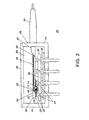
- a packaged photonics receiver module 24 including a monolithically integrated photonic receiver device 10 as taught by the present invention, a chip carrier 32, a conventional photonics package 28 and an optical fiber 30.
- the device or multiple devices 10 may be scribed to form a chip 38.
- the chip 38 is mounted to the chip carrier 32 and assembled with the optical fiber 30 into a standard metal or plastic device package 28, for example a dual in-line, ball grid array (BGA) or surface mount technique (SMT) device package.
- BGA ball grid array
- SMT surface mount technique
- the chip carrier 32 may be a standard chip carrier containing passive circuitry such as matching network circuitry.
- the chip 38 containing the photonic receiver device(s) 10 is mounted to a surface 40 of the chip carrier 32 such that the photoreceiver structure 14 is adjacent to the chip carrier surface 40.
- the rods 33 formed on the chip front side 16 each have an outer circumferential wall that comes into contact with one corresponding rod receptor 34 formed on the chip carrier 32.
- Each rod 33 is preferably formed from a material that is electrically conductive and compliant to thermally induced stresses, such as soft gold (Au). When the rod 33 and corresponding receptor 34 are aligned and brought together while applying heat and force, the rod 33 deforms and interlocks with its complementary receptor 34.
- the assembly that includes the photonic receiver device 10 and the chip carrier 32 is secured to a flat base 36 of the device package 28 using conventional techniques such as gold-tin (Au/Sn) alloyed solder so that the photonice receiver device back side 22 containing the fiber channel 20 is exposed.
- the flat base 36 may include a plurality of discrete electronic components and a plurality of interconnecting conductors attached thereto.
- the package 28 includes a generally tubular casing 42 attached to a package side wall 44 such that the tubular casing 42 extends horizontally through the side wall 44 into the package 28 to facilitate a conventional fiber pigtailing configuration.
- an extrusion portion (not shown) of the tubular casing 42 may be molded outside the wall 44 with flexible polypropylene rubber protect the fiber pigtail from being broken or otherwise disturbed.
- the optical fiber's 30 position within the fiber channel 20 allows it to passively assume an accurate optical alignment with the reflective mirror 18 and the photoreceiver structure 14 for efficient optical coupling of optical signals 17 transmitted from the fiber 30 and reflected at the mirror 18 to the photoreceiver structure 14. And, since the reflective mirror 18, the fiber channel 20 and the photoreceiver structure 14 are monolithically integrated from the same chip 12, optical misalignment between the optical fiber 30 and the photoreceiver structure 14 due to thermal fluctuations or mechanical stress is significantly reduced.
- a cover 48 is included for enclosing the package 28. The cover 48 is secured to the package side walls 44 at an opening 50 of the package 28 using conventional seam sealer or laser welder techniques suitable for use with metal device packages or plastic molding techniques suitable for use with plastic device packages.
- Fabrication of the photoreceiver structure 14 begins by preparing a semi-insulating semiconductor chip 12.
- the preferred chip material is semi-insulating indium phosphide (InP), chosen for its III-V crystal characteristics.
- the chip material may also be chosen from other semi-insulating III-V semiconductor materials including semi-insulating gallium arsenide (GaAs), semi-insulating gallium phosphide (GaP), semi-insulating indium arsenide (InAs), and semi-insulating indium phophide (InP).
- the chip 12 is first prepared on the front side surface 16 by a standard cleaning process that may include using 1-1-1 trichloroethylene (TCE), acetone (ACE), isopropanol (IPA), deionized water (DI) and potassium hydroxide (KOH) for indium-based chip materials or using hydrochloric acid (HCl) for gallium-based chip materials.
- a standard cleaning process may include using 1-1-1 trichloroethylene (TCE), ACE), isopropanol (IPA), deionized water (DI) and potassium hydroxide (KOH) for indium-based chip materials or using hydrochloric acid (HCl) for gallium-based chip materials.
- An alternative cleaning method for indium-based chip materials includes etching the front surface 16 of the chip 12 in a mixture of chromic acid and sulfuric acid followed by a deionized water (DI) rinse, a KOH soak, and finally a second DI rinse.
- DI deionized water
- the semiconductor chip 12 is rinsed in deionized water (DI) and then etched in a sulfuric acid:hydorperoxid:deionized water solution for approximately five to ten minutes, followed by a rinse in deionized water (DI) for approximately fifteen to thirty minutes. This etch removes the oxides and defect lattices from the chip 12 and the DI rinse removes the etchants from the chip 12.
- DI deionized water
- active layers 52 of the photoreceiver device structure 14 can be formed on the chip front side 16 using conventional epitaxial crystal growth processes. It is important to note that the device layer growth process required here is not limited to any particular process and can include molecular-electron beam epitaxial (MBE) crystal growth processes, metal organic chemical vapor deposition (MOCVD), liquid phase epitaxial crystal growth (LPE) processes, or other similarly suitable crystal growth processes.
- MBE molecular-electron beam epitaxial
- MOCVD metal organic chemical vapor deposition
- LPE liquid phase epitaxial crystal growth
- the remaining steps of the photoreceiver structure 14 fabrication process include photolighography and etching steps.
- VSLI very large scale integration
- the photolithography step includes coating a layer of photoresist material 54 over the epitaxially grown device layers 52 and soft baking the photoresist 54 at a temperature of from 90°C to 100°C for a period of approximately 45 minutes to provide a desired curvature in the photoresist material.
- a pattern mask 56 is aligned over the layer of photoresist material 54 and, using UV exposure, the mask pattern 56 is transferred to the photoresist layer 54.
- the transferred pattern as shown in FIG. 3E, is developed and the photoresist residue is removed using an oxygen plasma descum gas mixture, leaving a photoresist mask 58 on the epilayers 52 located at the chip front surface 16.
- the photoresist mask 58 enables the photoreceiver structure 14 to be formed into a mesa-like structure during subsequent etching steps
- the epitaxially grown layers 52 formed on the chip surface 16 are preferentially etched in those areas not protected by the photoresist mask 58 to form the mesa-shaped photoreceiver device structure 14.
- the epitaxially grown layers 52 on the chip 12 are wet-chemical etched using a suitable etchant such as a phosphoric acid:deionized water (H 3 PO 4 : H 2 O) solution, phosphoric acid:hydrogen peroxide (H 3 PO 4 :H 2 O 2 :H 2 0), succinic acid (H 2 0 2 :H 2 0) or similar acid or alkaline based solutions, depending on the material composition of the device structure 14.
- a suitable etchant such as a phosphoric acid:deionized water (H 3 PO 4 : H 2 O) solution, phosphoric acid:hydrogen peroxide (H 3 PO 4 :H 2 O 2 :H 2 0), succinic acid (H 2 0 2 :H 2 0) or
- the epilayers 52 may be dry etched using standard dry etch methods that may include electron cyclotron resonance etching (ECR) or reactive ion etching (RIE).
- ECR electron cyclotron resonance etching
- RIE reactive ion etching
- passivation and metallization steps are performed on the front side 16 of the chip 12.
- a "passivation" layer of a dielectric material is conventionally provided over the underlying device layers comprising integrated circuit structures.
- the passivation layer functions as an insulation layer and acts to protect the underlying structure from moisture and ion contamination that can damage or destroy the structure by causing corrosion and electrical shorts.
- the chip 12 is metallized to form electrical contacts and to form rod-shaped interconnections as taught by the Tran et al. cross-referenced patent application, "Apparatus and Method for Snap-On Thermo-Compression Bonding.”
- Each rod (see numerals 33, FIG. 3P) is formed on the chip front side 16 having an outer circumferential wall that comes into contact with a corresponding rod receptor (see numerals 34, FIG. 6) formed on a chip carrier (see numeral 32, FIG. 6).
- the rod 33 is preferably formed from a material that is electrically conductive and compliant to thermally induced stresses, such as soft gold (Au). When the rod 33 and complementary receptor 34 are aligned and brought together, the rod 33 deforms and interlocks with its complementary receptor 34. The attachment process occurs while applying heat and pressure (thermal compression), thereby forming a strong interlocking bond.
- the passivation step includes depositing a dielectric film 60 over the device structure 14 and the chip front surface 16.
- the preferred dielectric film material is silicon nitride and it may be deposited using chemical vapor deposition (CVD), electron beam (E-beam) deposition or a similar sputtering deposition method.
- the dielectric film material may include thin film dielectric materials such as silicon dioxide, silicon nitride, stacked silicon nitride or silicon dioxide layers, or other dielectric materials similarly impervious to moisture and other contaminants.
- the dielectric film deposition may also be accomplished by glass or polyimide spin-on methods. However, it is important to note that spin-methods are generally not as reliable as the deposition methods previously described.
- window regions 62 are created in the dielectric film layer 60 to facilitate the formation of electrical contact regions during subsequent metallization steps. These window regions 62 are created using photolithography and the dry etch techniques.
- the particular dry etch technique chosen here depends on the dielectric film material used during passivation. For example, RF plasma etch, DC plasma etch, reactive ion etch (RIE), electron cyclotron resonance radio frequency ion etch (ECR), and laser induced etch (LIE) are each etching techniques that can be used in combination with freon 14 (CF 4 ) or freon 22 (H 2 FC-CH 2 F) gases to etch silicon dioxide, silicon nitride, or similar dielectric thin film materials.
- freon 14 CF 4
- freon 22 H 2 FC-CH 2 F
- the metallization of the chip front side 16 begins by using photolithography steps to create a mask pattern for forming the electrical contact regions 66 (see FIG. 3K).
- the preferred photolithography method includes coating a thick layer of photoresist of from approximately two to six microns on the chip front side surface 16. Following a soft bake of the photoresist layer and prior to mask alignment, the photoresist layer is soaked in a chlorobenzen solution followed by UV exposure and a subsequent baking is applied to form a mask 64. It is important to note that this step does not require a particular photolithography technique and alternative methods such as double photoresist coating can be used.
- a metal deposition process is performed on the chip front side 16 using an e-beam or similar evaporation technique to form the electrical contact regions 66.
- a metal compound 68 that is metallurgically compatible with the top most semiconductor layer of the photoreceiver structure 14 is evaporated over the chip front side 16.
- the metal compound 68 is preferably a 400:1000:2000 angstrom thick contact metal compound such as Ti/Pt/Au, alloyed AuGe:Ni:Au or some similarly compatible metal compound, depending on the polarity of the contacts 66.
- lift-off of the photoresist mask 64 is performed by coating the chip front side 16 with an acetone spray or by soaking the surface 16 in a warm acetone solution for approximately ten minutes to two hours, or until all of the photoresist is lifted-off.
- the acetone acts to dissolve the photoresist mask material 64, leaving behind the electrical contact regions 66.
- the chip 12 is cleaned using an isopropanol (IPA) and deionized water (DI) solution.
- IPA isopropanol
- DI deionized water
- a thin film of aluminum 70 having a thickness of from approximately 1000 angstroms to 2000 angstroms is coated over the entire front side chip surface 16.
- the aluminum thin film 70 forms an electrically conductive layer used in the plating process described below.
- the formation of the rod contacts 33 begins by using photolithography steps to create a mask corresponding to the desired structure of the rod contacts 33.
- a layer of photoresist 72 having a thickness greater than the height of the mesa-shaped photoreceiver device structure 14, approximately 10 to 15 microns, is coated over the front surface 16 of the chip 12.
- a gold (Au) layer 74 is plated over the chip front side 16 at a thickness of from approximately five to nine microns higher than the mesa 14, thereby forming rod contacts 33.
- the photoresist layer 72 and the aluminum film 70 located beneath the photoresist 72 are removed from the chip front side 16 at once using conventional photoresist developer.
- the chip 12 is turned over to exposing the back-side 22 of the chip 12 and the chip 12 is mounted to a wafer carrier 76.
- a wafer carrier 76 As described in the Dean et al. cross-referenced application, "Optical Integrated Circuit Microbench System," a reflective mirror 18 and interacting channel 20 are formed on the chip back side 22.
- the chip 12 is demounted from the wafer carrier 76, cleaned using an isopropanol (IPA), trichloroethylene, or acetone solution, rinsed in a deionized water solution, and blown dry.
- IPA isopropanol
- acetone solution rinsed in a deionized water solution
- the mirror surface 18 is then vapor coated with a metal, preferrably Ti:Au, Ti:Ag or Al:Ag:Au, by slant mounting the chip 12 so that the reflective mirror 18 is exposed to the metal vapor, thus forming the mirror 18. Finally, the chip 12 is again lifted off the wafer carrier 76 and cleaned using techniques previously described.
- a metal preferrably Ti:Au, Ti:Ag or Al:Ag:Au
- the chip 12 may be cut using a diamond scribe process or similar process to form a chip 38 containing active electronic circuitry 80 such as MMIC, HBT or HEMT circuitry and one or many monolithic photoreceiver devices 10.
- FIG. 5A shows a top view illustration of such a chip 38 containing multiple devices 10.
- FIG. 5B shows a bottom view illustration of the chip 38 illustrated n FIG. 5A, and
- FIGs. 5C and 5D respectively show exploded cross section and top view illustrations of a monolithic receiver device 10 contained in the chip 38.
- Each rod receptor 34 is generally cylindrically shaped with a hollow middle portion that when plated on the chip carrier 32 forms a centrally disposed well for receiving a rod 33 (not shown).
- a lip portion 35 is formed on an end or mouth of the rod receptor 34 for interlocking engagement with the rod 33.
- the rod receptor 34 is preferably manufactured from a material that is conductive and compliant to thermally induced stresses, such as soft gold (Au).
- the chip 38 is flip-chip bonded to the chip carrier 32 to form a submodule 90, wherein each rod 33 is axially aligned with a corresponding rod receptor 34 and brought into contact with the rod receptor 34.
- the rod 33 and the rod receptor 34 are then pushed or snapped together, causing the rod 33 to deform and interlock with the rod receptor 34.
- the end of the rod 33 engages the well portion of the rod receptor 34 housing, causing the outside wall of the rod 33 to spread out and curl under the lip portion of the rod receptor 34, thus securely interlocking the rod 33 into the rod receptor 34 and correspondingly the photonic receiver device device 10 to the chip carrier 32.
- This connection process preferably a thermo-compression bonding process, occurs while applying heat and force, thereby producing a strong interlocking bond.
- the submodule 90 is packaged into a universal (standard) metal or plastic package 28 such as a dual in-line, ball grid array (BGA) or surface mount technique (SMT) package.
- the submodule 90 as shown in FIG. 9, is secured to a base 36 of the package housing using a gold-tin (Au/Sn) eutectic solder or similar technique.
- Au/Sn gold-tin
- an optical fiber 30 is positioned in the fiber channel 20 of the submodule 90 by extending the fiber 30 through a tubular casing 42 mounted at a side wall 44 of the package 28.
- the optical fiber 30 is secured in the fiber channel 20 using fiber assembly techniques such as hermetic Au/Sn eutectic solder or epoxy attachment.
- a package cover 48 is sealed in an opening 50 of the package 28 using seam sealer, laser welder or plastic molding.
- the monolithic photonic receiver device technology previously described can be applied to all electronic devices used for space, avionics and commercial applications that may use amplifiers, receivers and transmitter devices.
- arrays of photonic receiver devices can be fabricated and flip-chip attached to devices to produce highly reliable and low-cost electro-optic assemblies.
Landscapes
- Physics & Mathematics (AREA)
- General Physics & Mathematics (AREA)
- Optics & Photonics (AREA)
- Light Receiving Elements (AREA)
- Optical Couplings Of Light Guides (AREA)
- Electrodes Of Semiconductors (AREA)
Applications Claiming Priority (2)
| Application Number | Priority Date | Filing Date | Title |
|---|---|---|---|
| US65460400A | 2000-09-01 | 2000-09-01 | |
| US654604 | 2000-09-01 |
Publications (1)
| Publication Number | Publication Date |
|---|---|
| EP1189087A2 true EP1189087A2 (fr) | 2002-03-20 |
Family
ID=24625528
Family Applications (1)
| Application Number | Title | Priority Date | Filing Date |
|---|---|---|---|
| EP20010117690 Withdrawn EP1189087A2 (fr) | 2000-09-01 | 2001-07-26 | Récepteur photonique monolithique comprenant un support de fibre autoaligné adapté pour assemblage du type flip chip |
Country Status (2)
| Country | Link |
|---|---|
| EP (1) | EP1189087A2 (fr) |
| JP (1) | JP2002122760A (fr) |
Cited By (3)
| Publication number | Priority date | Publication date | Assignee | Title |
|---|---|---|---|---|
| WO2004042829A1 (fr) * | 2002-11-07 | 2004-05-21 | Koninklijke Philips Electronics N.V. | Photodetecteur inverse |
| WO2004102682A1 (fr) * | 2003-05-13 | 2004-11-25 | Raytheon Company | Technique de passivation de photodiodes |
| CN103217740A (zh) * | 2012-01-18 | 2013-07-24 | 国际商业机器公司 | 硅光子芯片光学耦合结构 |
Families Citing this family (1)
| Publication number | Priority date | Publication date | Assignee | Title |
|---|---|---|---|---|
| US6985645B2 (en) * | 2003-09-24 | 2006-01-10 | International Business Machines Corporation | Apparatus and methods for integrally packaging optoelectronic devices, IC chips and optical transmission lines |
-
2001
- 2001-07-26 EP EP20010117690 patent/EP1189087A2/fr not_active Withdrawn
- 2001-08-21 JP JP2001249965A patent/JP2002122760A/ja active Pending
Cited By (5)
| Publication number | Priority date | Publication date | Assignee | Title |
|---|---|---|---|---|
| WO2004042829A1 (fr) * | 2002-11-07 | 2004-05-21 | Koninklijke Philips Electronics N.V. | Photodetecteur inverse |
| WO2004102682A1 (fr) * | 2003-05-13 | 2004-11-25 | Raytheon Company | Technique de passivation de photodiodes |
| US7030032B2 (en) | 2003-05-13 | 2006-04-18 | Raytheon Company | Photodiode passivation technique |
| CN103217740A (zh) * | 2012-01-18 | 2013-07-24 | 国际商业机器公司 | 硅光子芯片光学耦合结构 |
| US8855452B2 (en) | 2012-01-18 | 2014-10-07 | International Business Machines Corporation | Silicon photonic chip optical coupling structures |
Also Published As
| Publication number | Publication date |
|---|---|
| JP2002122760A (ja) | 2002-04-26 |
Similar Documents
| Publication | Publication Date | Title |
|---|---|---|
| US7479401B2 (en) | Front side illuminated photodiode with backside bump | |
| US6219470B1 (en) | Wavelength division multiplexing transmitter and receiver module | |
| US6115521A (en) | Fiber/waveguide-mirror-lens alignment device | |
| US6999493B2 (en) | Surface emission laser and manufacturing method for surface emission laser, light reception element and manufacturing method for light reception element, and optical transceiver module | |
| EP0331331B1 (fr) | Sous-élément pour composants opto-électroniques | |
| US6994479B2 (en) | Substrate, optical fiber connection end member, optical element housing member, and method of fabrication of an optical module and the substrate | |
| US20060239612A1 (en) | Flip-chip devices formed on photonic integrated circuit chips | |
| US7968429B2 (en) | Method of manufacturing a semiconductor photodetector device by removing the semiconductor substrate on one surface after forming the light-transmitting layer on the opposing surface | |
| EP0541386A1 (fr) | Structure de circuit d'interconnexion optique | |
| US7309171B2 (en) | Optical bond-wire interconnections and a method for fabrication thereof | |
| US6187515B1 (en) | Optical integrated circuit microbench system | |
| US20030123508A1 (en) | Integral vertical cavity surface emitting laser and power monitor | |
| US20030098511A1 (en) | Flip-chip-bonded optical module package and method of packaging optical module using flip chip bonding | |
| EP1189087A2 (fr) | Récepteur photonique monolithique comprenant un support de fibre autoaligné adapté pour assemblage du type flip chip | |
| US20140029890A1 (en) | Optical system with integrated photodetectors | |
| US7482184B2 (en) | Manufacture of a layer of optical interconnection on an electronic circuit | |
| JPH0774341A (ja) | 光電子集積回路装置の製造方法 | |
| US12038610B2 (en) | Wafer-level optoelectronic packaging | |
| Joo et al. | Fabrication of optical Tx/Rx subscriber modules incorporating passive alignment technique | |
| JPH1090540A (ja) | 半導体受光素子、半導体受光装置および半導体装置 | |
| KR20150020278A (ko) | 전자, 광전자, 광학 또는 광자 컴포넌트를 위한 서브마운트 | |
| KR100243411B1 (ko) | 반도체 레이저와 광검출기가 단일칩 집적된 양방향 광소자 구조및 제조 방법 | |
| JP2005093722A (ja) | 光機能素子および光機能素子の製造方法 | |
| KR100472382B1 (ko) | 평면도파로형광회로모듈및그제조방법 | |
| Joo et al. | Optical coupling of a SMF to flip-chip bonded laser diode for low-cost subscriber's transmitter module |
Legal Events
| Date | Code | Title | Description |
|---|---|---|---|
| PUAI | Public reference made under article 153(3) epc to a published international application that has entered the european phase |
Free format text: ORIGINAL CODE: 0009012 |
|
| AK | Designated contracting states |
Kind code of ref document: A2 Designated state(s): AT BE CH CY DE DK ES FI FR GB GR IE IT LI LU MC NL PT SE TR |
|
| AX | Request for extension of the european patent |
Free format text: AL;LT;LV;MK;RO;SI |
|
| STAA | Information on the status of an ep patent application or granted ep patent |
Free format text: STATUS: THE APPLICATION HAS BEEN WITHDRAWN |
|
| 18W | Application withdrawn |
Effective date: 20020819 |
|
| R18W | Application withdrawn (corrected) |
Effective date: 20030819 |