EP1191603A2 - MOS-Bauelement mit Graben und Randabschluss - Google Patents
MOS-Bauelement mit Graben und Randabschluss Download PDFInfo
- Publication number
- EP1191603A2 EP1191603A2 EP01122746A EP01122746A EP1191603A2 EP 1191603 A2 EP1191603 A2 EP 1191603A2 EP 01122746 A EP01122746 A EP 01122746A EP 01122746 A EP01122746 A EP 01122746A EP 1191603 A2 EP1191603 A2 EP 1191603A2
- Authority
- EP
- European Patent Office
- Prior art keywords
- trench
- layer
- termination structure
- semiconductor substrate
- mos
- Prior art date
- Legal status (The legal status is an assumption and is not a legal conclusion. Google has not performed a legal analysis and makes no representation as to the accuracy of the status listed.)
- Withdrawn
Links
Images



Classifications
-
- H—ELECTRICITY
- H10—SEMICONDUCTOR DEVICES; ELECTRIC SOLID-STATE DEVICES NOT OTHERWISE PROVIDED FOR
- H10D—INORGANIC ELECTRIC SEMICONDUCTOR DEVICES
- H10D30/00—Field-effect transistors [FET]
- H10D30/60—Insulated-gate field-effect transistors [IGFET]
- H10D30/64—Double-diffused metal-oxide semiconductor [DMOS] FETs
- H10D30/66—Vertical DMOS [VDMOS] FETs
- H10D30/668—Vertical DMOS [VDMOS] FETs having trench gate electrodes, e.g. UMOS transistors
-
- H—ELECTRICITY
- H10—SEMICONDUCTOR DEVICES; ELECTRIC SOLID-STATE DEVICES NOT OTHERWISE PROVIDED FOR
- H10D—INORGANIC ELECTRIC SEMICONDUCTOR DEVICES
- H10D12/00—Bipolar devices controlled by the field effect, e.g. insulated-gate bipolar transistors [IGBT]
- H10D12/01—Manufacture or treatment
- H10D12/031—Manufacture or treatment of IGBTs
- H10D12/032—Manufacture or treatment of IGBTs of vertical IGBTs
- H10D12/038—Manufacture or treatment of IGBTs of vertical IGBTs having a recessed gate, e.g. trench-gate IGBTs
-
- H—ELECTRICITY
- H10—SEMICONDUCTOR DEVICES; ELECTRIC SOLID-STATE DEVICES NOT OTHERWISE PROVIDED FOR
- H10D—INORGANIC ELECTRIC SEMICONDUCTOR DEVICES
- H10D12/00—Bipolar devices controlled by the field effect, e.g. insulated-gate bipolar transistors [IGBT]
- H10D12/411—Insulated-gate bipolar transistors [IGBT]
- H10D12/441—Vertical IGBTs
- H10D12/461—Vertical IGBTs having non-planar surfaces, e.g. having trenches, recesses or pillars in the surfaces of the emitter, base or collector regions
- H10D12/481—Vertical IGBTs having non-planar surfaces, e.g. having trenches, recesses or pillars in the surfaces of the emitter, base or collector regions having gate structures on slanted surfaces, on vertical surfaces, or in grooves, e.g. trench gate IGBTs
-
- H—ELECTRICITY
- H10—SEMICONDUCTOR DEVICES; ELECTRIC SOLID-STATE DEVICES NOT OTHERWISE PROVIDED FOR
- H10D—INORGANIC ELECTRIC SEMICONDUCTOR DEVICES
- H10D30/00—Field-effect transistors [FET]
- H10D30/60—Insulated-gate field-effect transistors [IGFET]
- H10D30/64—Double-diffused metal-oxide semiconductor [DMOS] FETs
- H10D30/66—Vertical DMOS [VDMOS] FETs
- H10D30/665—Vertical DMOS [VDMOS] FETs having edge termination structures
-
- H—ELECTRICITY
- H10—SEMICONDUCTOR DEVICES; ELECTRIC SOLID-STATE DEVICES NOT OTHERWISE PROVIDED FOR
- H10D—INORGANIC ELECTRIC SEMICONDUCTOR DEVICES
- H10D62/00—Semiconductor bodies, or regions thereof, of devices having potential barriers
- H10D62/10—Shapes, relative sizes or dispositions of the regions of the semiconductor bodies; Shapes of the semiconductor bodies
- H10D62/102—Constructional design considerations for preventing surface leakage or controlling electric field concentration
- H10D62/103—Constructional design considerations for preventing surface leakage or controlling electric field concentration for increasing or controlling the breakdown voltage of reverse-biased devices
- H10D62/104—Constructional design considerations for preventing surface leakage or controlling electric field concentration for increasing or controlling the breakdown voltage of reverse-biased devices having particular shapes of the bodies at or near reverse-biased junctions, e.g. having bevels or moats
-
- H—ELECTRICITY
- H10—SEMICONDUCTOR DEVICES; ELECTRIC SOLID-STATE DEVICES NOT OTHERWISE PROVIDED FOR
- H10D—INORGANIC ELECTRIC SEMICONDUCTOR DEVICES
- H10D64/00—Electrodes of devices having potential barriers
- H10D64/111—Field plates
-
- H—ELECTRICITY
- H10—SEMICONDUCTOR DEVICES; ELECTRIC SOLID-STATE DEVICES NOT OTHERWISE PROVIDED FOR
- H10D—INORGANIC ELECTRIC SEMICONDUCTOR DEVICES
- H10D64/00—Electrodes of devices having potential barriers
- H10D64/111—Field plates
- H10D64/117—Recessed field plates, e.g. trench field plates or buried field plates
-
- H—ELECTRICITY
- H10—SEMICONDUCTOR DEVICES; ELECTRIC SOLID-STATE DEVICES NOT OTHERWISE PROVIDED FOR
- H10D—INORGANIC ELECTRIC SEMICONDUCTOR DEVICES
- H10D8/00—Diodes
- H10D8/01—Manufacture or treatment
- H10D8/051—Manufacture or treatment of Schottky diodes
-
- H—ELECTRICITY
- H10—SEMICONDUCTOR DEVICES; ELECTRIC SOLID-STATE DEVICES NOT OTHERWISE PROVIDED FOR
- H10D—INORGANIC ELECTRIC SEMICONDUCTOR DEVICES
- H10D8/00—Diodes
- H10D8/60—Schottky-barrier diodes
-
- H—ELECTRICITY
- H10—SEMICONDUCTOR DEVICES; ELECTRIC SOLID-STATE DEVICES NOT OTHERWISE PROVIDED FOR
- H10D—INORGANIC ELECTRIC SEMICONDUCTOR DEVICES
- H10D8/00—Diodes
- H10D8/60—Schottky-barrier diodes
- H10D8/605—Schottky-barrier diodes of the trench conductor-insulator-semiconductor barrier type, e.g. trench MOS barrier Schottky rectifiers [TMBS]
Definitions
- the present invention is related to a semiconductor device, specifically, to a novel termination structure for trench MOS devices so as to prevent leakage current.
- Doubled diffused metal-oxide-semiconductor field effect transistor (DMOSFET), insulated gate bipolar transistor (IGBT), and Schottky diode are important power devices and use extensively as output rectifiers in switching-mode power supplies and in other high-speed power switching applications.
- the applications include motor drives, switching of communication device, industry automation and electronic automation.
- the power devices are usually required carrying large forward current, high reverse-biased blocking voltage, such as above 30 volt, and minimizing the reverse-biased leakage current.
- trench DMOS, trench IGBT and trench Schottky diode are superior to those of with planar structure.
- LOCOS local oxidation of silicon
- field plate field plate
- guard ring guard ring
- leakage current is increased and electrical properties of the active region are deteriorated.
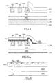
- FIG.1 a semiconductor substrate with trench MOS structure for Schottky diodes, and a trench termination structure formed therein.
- the substrate is a heavily doped n+ substrate 10 and an epitaxial layer 20 formed thereon.
- the trench MOS devices including epitaxial layer 20/gate oxide layer 25/ polysilicon layer 30 are formed in the active region 5.
- the boundary of the active region 5 to the edge of the die is a LOCOS region of about 6000 ⁇ in thick formed by conventional method.
- a p+-doping region 50 beneath LOCOS region is formed through ion implantation.
- the p+-doping region 50 is as a guard ring for reverse-biased blocking voltage enhancement.
- the anode (a metal layer) 55 is formed on the active region 5 and extends over p+ doping region 50 of LOCOS region. The object is to make the bending region of the depletion boundary far away from the active region 5.
- guard ring 50 can alleviate the electrical field crowding and relax the bending magnitude occurred near the active region, the adjacent region between p+ region 50 and beneath the bottom of the trench MOS device, as arrow indicated denoted by 60, is not a smooth curve.
- An object of the present invention thus proposes a novel termination structure.
- the new termination structure made the bending region of the depletion region far away from the active region, and depletion boundary is flatter than forgoing prior art.
- the manufacturing method provided by the present invention is even simpler than those prior arts. Since the termination structure and trench are formed simultaneously, it requires only three photo masks, low complicated processes and low cost.
- the present invention discloses a novel termination structure, which can be formed with trench MOS devices simultaneously.
- the MOS devices can be Schottky diode, DMOS or IGBT depending on what kinds of the semiconductor substrate are prepared.
- the termination structure and trench MOS devices comprising: a semiconductor substrate having a plurality of first trenches spaced each other and formed in an active region and having a second trench formed from a boundary of the active region to an end of the semiconductor substrate; a first-type MOS gate formed in each of the first trenches, and a second MOS gate as a spacer formed on a sidewall of the second trench; a termination structure oxide layer formed in the second trench to cover a portion of the spacer and to cover a bottom of the second trench; and a first electrode and a second electrode are, respectively, formed on a bottom surface and upper surface of the semiconductor substrate.
- the second electrode is located to cover the region from the active region through the spacer to a portion of the termination structure oxide layer so that a bending portion of the
- the conventional termination structure including local oxidation, electric field plate, guard ring, or the combination thereof, all of them do not solve completely the electric field crowding issues.
- the field crowding may still occur at different positions, depending on the design difference.
- the present invention proposes a novel trench termination structure and a method to make them.
- the novel trench termination structure is to overcome problems of electric field crowding issues.
- the newly trench termination provides a flat depletion boundary, and the bending region thereof is far away from the active region while encountered a reverse-bias voltage. Consequently, the novel termination structure can prevent breakdown phenomena from being occurred prematurely.
- the newly termination structure can be applied to any power transistors such as Schottky rectifier, DMOS, IGBT etc..
- the trench MOS devices can be formed with the trench termination structure simultaneously.
- the first preferred embodiment is to illustrate the method of forming trench termination structure and the Schottky diode simultaneously.
- a cross-sectional view shows a semiconductor substrate 100 comprised a first layer 100A having a first kind of conductive impurity doped (for example type n) and a base substrate 100B having a first kind of conductive impurity heavily doped (for example n+).
- First layer 100A is formed epitaxially on the base substrate 100B for forming Schottky contact and the base substrate is for forming ohmic contact while metal layers are formed thereon.
- An oxide layer 101 is then formed on the first substrate 100A by CVD to about 2000 ⁇ - 10000 ⁇ .
- a photoresist (not shown) is coated on the oxide layer 101 to define a plurality of first trenches 110 and a second trench 120.
- Each of the first trenches 110 is about 0.2-2.0 ⁇ m in width from cross-sectional view formed in the active region.
- the second trench 120 is spaced by a mesa 115 to the first trench 110 and formed from the boundary of the active region to an end of a semiconductor substrate 100 (or a die).
- the second trench 120 is to make depletion boundary flat and prevent electric field crowding.
- a high temperature oxidation process to form gate oxide layer 125 is performed.
- the gate oxide layer 125 with a thickness between about 150 ⁇ to 3000 ⁇ is formed on the sidewalls 110A, 120A, bottoms 110B, 120B of the first and second trench 110, 120, and the mesa surface 115A.
- the gate oxide layer 125 can be formed by high temperature deposition to form HTO (high temperature oxide deposition) layer.
- a first conductive layer 140 is formed by CVD on the gate oxide 125 and refilled the first trench 110 and the second trench 120, and at least with a height higher than the mesa115.
- the first conductive layer 140 is also formed on the backside of the semiconductor substrate 100E due to the CVD process.
- the first conductive layer is material selected from the group consisting of metal, polysilicon and amorphous silicon.
- the first conductive layer 140 is about 0.5 to 3.0 ⁇ m.
- the polysilicon layer formed by LPCVD (low pressure CVD) which has good step coverage is preferred as the material of the first layer 140.
- amorphous silicon by PECVD would be preferred.
- the amorphous silicon has better gap filled characteristic than polysilicon. Hence, to make it with conductive properties, an amorphous silicon recrystallized process is needed.
- an anisotropic etching is done to remove the excess first conductive layer 140 above the mesa surface 115A using the gate oxide layer 125 on the mesa 115 as an etching stop layer.
- a spacer 122 having a width (along cross-sectional view) about the same as the height of the second trench is formed on the sidewall 125A of the second trench 120.
- the dielectric layer 150 for termination structure is a TEOS layer either LPTEOS or PETEOS or O 3 - TEOS or HTO layer.
- the dielectric layer 150 is between about 0.2-1.0 ⁇ m.
- a photoresist pattern 155 is coated on the dielectric layer 150 so as to define ranges of Schottky contacts. And then a dry etching using photoresist pattern 155 as a mask is carried out to expose mesa surface 115A and first conductive layer 140 of the first trench 110.
- a backside unwanted layer removal is implemented to expose surface of the base substrate 100B.
- the unwanted layers are those layers formed on the backside of semiconductor substrate due to thermal oxidation process or CVD process for fabricating devices in the active region, including dielectric layer 150, first conductive layer 140, and gate oxide layer 125.
- anode 160A is formed from active region extending to the second trench 120 and at least to a region away from the active region by 2.0 ⁇ m. So the bending region of the depletion region is able to be far away from the active region.
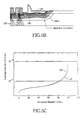
- FIG. 5B shows one of the electric properties of the trench MOS termination structure (shown in FIG. 5A).
- the cathode 160 has, for example, 100 Volt and anode 183 has 0 Volt.
- the numeral 180 denotes equipotential lines.
- the voltages burdened by the equipotential lines from bottom to up are gradually decreased.
- the lines perpendicular to the equipotential lines 180 represent lines of electrical force.
- leakage current only generates in the active region and almost none in the depletion region under termination region.
- the boundary of depletion region, denoted by label 180A gives flat characteristic, and thus the voltage breakdown premature would not occur. It gives only a little bit of leakage current.
- FIG.5C shows a comparison for reversed current curves of the trench MOS structure without termination structure 195 and with the termination structure 190 in accordance with the present invention.
- the termination structure merely increases reversed current by 8.8%.
- the LOCOS combines with guard ring structure.
- the present invention gives significant improvement.
- it requires at least 4 photo masks by conventional manufacture processes compared to three masks only in the present invention (e.g., forming trench (1 st ), contact definition (2 nd ), and the second conductive layer etching to form anode (3 rd )).
- the present invention gives a simpler process.
- the second preferred embodiment using the termination structure according to the present invention is to form trench DMOS structure and termination structure.
- a semiconductor substrate 200 from the top to the bottom comprises a first layer 200A, a second layer 200B and a base substrate 200C.
- the first layer 200A and the second layer are formed on the base substrate 200C by epitaxial processes.
- the first layer 200A having a p-type conductive doped impurities as a base layer and then a doping layer 203 with p-type conductive heavily doped impurities on the top portion of the first layer 200A.
- the second layer 200B is with n-type conductive doped impurities, and the third layer 200C with n-type conductive heavily doped impurities.
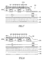
- a plurality of n+ regions are formed in the upper portion of the first layer 200A to cut p+ layer 203 to be as many n+ regions 204 and p+ region 204 by ion implantation, as is shown in FIG.6.
- the thickness of the first and second layer 200A and 200B are 0.5 ⁇ m - 5.0 ⁇ m and 3 ⁇ m - 30 ⁇ m, respectively.
- a plurality of the first trenches 210 and the second trench 220 having a mesa 215 in between are formed firstly.
- the first trenches 210 are formed in the active region, through n+ regions 204.
- the second trench 220 is formed in the region from the boundary of the active region to an end of the semiconductor substrate 200 (or a die).
- a high temperature oxidation process is performed to form a gate oxide layer 225 with a thickness of between about 150 ⁇ to 3000 ⁇ .
- a conductive layer 240 selected from first polysilicon or amorphous silicon is refilled to the first trenches 210 and the second trench 220 and over mesa 215.
- An etching back step is then carried out to remove excess conductive layer 240 using gate oxide layer 225 on the surface of mesa 215A as a stopping layer.
- the gate oxide layer 225 removal above mesa is then followed using the n+ region 204 and the p+ region 203 as a stopping layer.
- an inter-conductive oxide layer 245 by oxidizing a portion of the first conductive layer 240. Since the grain boundaries of the polysilicon can provide oxygen fast diffusion paths, the oxide layer formed by the polysilicon or amorphous silicon in the first trenches 210 and the second trench 220 are much thicker than that on the semiconductor substrate, the mesa surface 215A.
- an etching back step is performed to remove thermal oxide layer 245 above surface of the first layer 200A, the n+ region 204 and p+ region 203.
- thermal oxide layer 245 on the spacer 240 of the second trench 220 and on the cop surface of first conductive layer 240 after this step to provide isolation function.
- a TEOS oxide layer 250 is then formed on all areas.
- a photoresist pattern is then formed on TEOS oxide layer 250 of the first layer 200A to define source contact regions.
- the unwanted layers formed on the backside of semiconductor substrate are removed firstly.
- the unwanted layers includes TEOS oxide layer 250, inter-conductive oxide layer 245, first conductive layer 240 and gate oxide layer 225 on the surface of base substrate 200C, which are formed simultaneously while making the devices in the active region.
- a metal layer 260 deposition by sputtering is performed to form source contact on the first layer 200A and drain contact on the base substrate 200C i.e. the backside of the semiconductor substrate.
- the metal layer 260 formed on the active region is still required to extend to the termination structure 220 by a distance at least about 2.0 ⁇ m so as to distant from the active region.
- a lithographic and an etching process are successively carried out as before.
- the third preferred embodiment using the termination structure according to the present invention is to form trench IGBT structure and termination structure simultaneously.
- a semiconductor substrate 300 prepared from the top to the bottom comprises a first layer 300A, a second layer 300B, a third layer 300C and a base substrate 300D.
- the first layer 300A, the second layer 300B, and third layers 300C, are formed on the base substrate 300D by epitaxial processes.
- first layer 300A, 300B and 300C having doping type, and doping concentration similar to the semiconductor substrate shown in FIG.6.
- first layer 300A is p-type base layer having upper portion n+ regions 304 and p + regions 303 in the upper portion of the p-base layer 302.
- the second layer 300B is a n- doping layer as a drift region and third layer 300C is a n+ layer 300B as a buffer layer.
- the base substrate 300D is, however, a p-type conductive impurities heavily doped region.
- the thickness of the first and the second layer 300A and 300B are 0.5 ⁇ m - 10.0 ⁇ m and 3 ⁇ m - 100 ⁇ m, respectively.
- a plurality of the first trenches 310 are formed through the n+-doped region 304.
- the bottom of the first trenches 310 comes down to below the layer of the p-type-doped layer 302.
- the second trench 320 and first trench individual, each is spaced by a mesa 315 having 0.2 to 4.0 ⁇ m.
- the second trench 320 is formed at the boundary of the active region and is extended to an edge of the semiconductor substrate.
- a refilled process with the first conductive material 340 such as polysilicon or amorphous silicon layer is deposited on the first trenches 310 and the second trench 320.
- An etch back process is then performed using gate oxide layer 325 on the surface of the mesa 315 as a stopping layer so that only the first trenches 310 and spacer in the second trench have the first conductive material 340.
- gate oxide layer 325 on the surface of the first layer is then removed and then another thermal oxidation process is carried out to form inter-conductive oxide layer 345 for the conductive layer 340 and the metal layer (formed later) isolation. Thereafter, the thermal oxide 345 above mesa surface 315A is removed but a portion of the thermal oxide layer, which is on the first conductive layer in the first trenches 310 and the second trench 320 are remaining as an inter-conductive oxide layer.
- a TEOS dielectric layer 350 deposition on all areas and photoresist pattern coating are followed successively as before. Thereafter, an etching process is implemented to expose the n+-doped region 204 arid the p+-doped region.
- FIG.12 shows backside unwanted layers on base substrate are removed before metal sputtering.
- a metal layer is formed on a surface of base substrate 300D to form collector electrode.
- the emitter electrode is formed on the surface of 300A, which contacts the p+ region 303 and n+ region 304. One end of emitter electrode is located at a distance away from active region.
Landscapes
- Electrodes Of Semiconductors (AREA)
Applications Claiming Priority (2)
| Application Number | Priority Date | Filing Date | Title |
|---|---|---|---|
| US668663 | 2000-09-22 | ||
| US09/668,663 US6396090B1 (en) | 2000-09-22 | 2000-09-22 | Trench MOS device and termination structure |
Publications (2)
| Publication Number | Publication Date |
|---|---|
| EP1191603A2 true EP1191603A2 (de) | 2002-03-27 |
| EP1191603A3 EP1191603A3 (de) | 2004-11-17 |
Family
ID=24683263
Family Applications (1)
| Application Number | Title | Priority Date | Filing Date |
|---|---|---|---|
| EP01122746A Withdrawn EP1191603A3 (de) | 2000-09-22 | 2001-09-21 | MOS-Bauelement mit Graben und Randabschluss |
Country Status (4)
| Country | Link |
|---|---|
| US (1) | US6396090B1 (de) |
| EP (1) | EP1191603A3 (de) |
| JP (2) | JP4702822B2 (de) |
| CN (1) | CN1209822C (de) |
Cited By (6)
| Publication number | Priority date | Publication date | Assignee | Title |
|---|---|---|---|---|
| WO2004107448A1 (en) * | 2003-05-31 | 2004-12-09 | Koninklijke Philips Electronics N.V. | Semiconductor device having an edge termination structure and method of manufacture thereof |
| EP1543554A4 (de) * | 2002-07-11 | 2008-05-07 | Int Rectifier Corp | Graben-schottky-barrieren-diode |
| US7754550B2 (en) | 2003-07-10 | 2010-07-13 | International Rectifier Corporation | Process for forming thick oxides on Si or SiC for semiconductor devices |
| EP2801114A4 (de) * | 2012-01-04 | 2015-08-26 | Vishay Gen Semiconductor Llc | Graben-dmos-vorrichtung mit verbesserter anschlussstruktur für hochspannungsanwendungen |
| EP2879168A4 (de) * | 2012-07-26 | 2016-03-02 | Csmc Technologies Fab1 Co Ltd | Verfahren zur entfernung einer schutzschicht aus polykristallinem silicium auf einer igbt-rückseite mit feldkonfektionierung |
| CN109585572A (zh) * | 2018-12-29 | 2019-04-05 | 矽力杰半导体技术(杭州)有限公司 | 半导体器件及其制造方法 |
Families Citing this family (50)
| Publication number | Priority date | Publication date | Assignee | Title |
|---|---|---|---|---|
| US6396090B1 (en) * | 2000-09-22 | 2002-05-28 | Industrial Technology Research Institute | Trench MOS device and termination structure |
| GB2381122B (en) * | 2001-10-16 | 2006-04-05 | Zetex Plc | Termination structure for a semiconductor device |
| JP3631464B2 (ja) * | 2001-12-27 | 2005-03-23 | 株式会社東芝 | 半導体装置 |
| US6828649B2 (en) * | 2002-05-07 | 2004-12-07 | Agere Systems Inc. | Semiconductor device having an interconnect that electrically connects a conductive material and a doped layer, and a method of manufacture therefor |
| CN100479187C (zh) * | 2003-01-29 | 2009-04-15 | 国际整流器有限公司 | 槽沟mosfet技术在直流-直流变换器中的应用 |
| US7009228B1 (en) * | 2003-03-04 | 2006-03-07 | Lovoltech, Incorporated | Guard ring structure and method for fabricating same |
| US6958275B2 (en) * | 2003-03-11 | 2005-10-25 | Integrated Discrete Devices, Llc | MOSFET power transistors and methods |
| US6987305B2 (en) * | 2003-08-04 | 2006-01-17 | International Rectifier Corporation | Integrated FET and schottky device |
| KR100964400B1 (ko) * | 2003-10-01 | 2010-06-17 | 삼성전자주식회사 | 반도체 소자의 콘택 구조체 |
| CN100505302C (zh) * | 2003-12-24 | 2009-06-24 | 丰田自动车株式会社 | 沟槽栅极场效应器件 |
| CN101421832A (zh) * | 2004-03-01 | 2009-04-29 | 国际整流器公司 | 沟槽器件的自对准接触结构 |
| US6927451B1 (en) * | 2004-03-26 | 2005-08-09 | Siliconix Incorporated | Termination for trench MIS device having implanted drain-drift region |
| JP2006120789A (ja) * | 2004-10-20 | 2006-05-11 | Toshiba Corp | 半導体装置 |
| US7598576B2 (en) * | 2005-06-29 | 2009-10-06 | Cree, Inc. | Environmentally robust passivation structures for high-voltage silicon carbide semiconductor devices |
| US7525122B2 (en) * | 2005-06-29 | 2009-04-28 | Cree, Inc. | Passivation of wide band-gap based semiconductor devices with hydrogen-free sputtered nitrides |
| US7855401B2 (en) * | 2005-06-29 | 2010-12-21 | Cree, Inc. | Passivation of wide band-gap based semiconductor devices with hydrogen-free sputtered nitrides |
| US7750398B2 (en) * | 2006-09-26 | 2010-07-06 | Force-Mos Technology Corporation | Trench MOSFET with trench termination and manufacture thereof |
| US7560355B2 (en) * | 2006-10-24 | 2009-07-14 | Vishay General Semiconductor Llc | Semiconductor wafer suitable for forming a semiconductor junction diode device and method of forming same |
| US8017494B2 (en) * | 2007-01-31 | 2011-09-13 | International Rectifier Corporation | Termination trench structure for mosgated device and process for its manufacture |
| KR100861213B1 (ko) * | 2007-04-17 | 2008-09-30 | 동부일렉트로닉스 주식회사 | 반도체 소자 및 그 제조방법 |
| US8269265B2 (en) * | 2008-07-14 | 2012-09-18 | Microsemi Semiconductor (U.S.) Inc. | Trench capacitor for high voltage processes and method of manufacturing the same |
| JP2010098189A (ja) * | 2008-10-17 | 2010-04-30 | Toshiba Corp | 半導体装置 |
| US20110084332A1 (en) * | 2009-10-08 | 2011-04-14 | Vishay General Semiconductor, Llc. | Trench termination structure |
| JP5531620B2 (ja) * | 2010-01-05 | 2014-06-25 | 富士電機株式会社 | 半導体装置 |
| CN101853854B (zh) * | 2010-03-12 | 2012-11-21 | 无锡新洁能功率半导体有限公司 | 一种改进型终端结构的沟槽功率mos器件 |
| US8853770B2 (en) * | 2010-03-16 | 2014-10-07 | Vishay General Semiconductor Llc | Trench MOS device with improved termination structure for high voltage applications |
| US8928065B2 (en) | 2010-03-16 | 2015-01-06 | Vishay General Semiconductor Llc | Trench DMOS device with improved termination structure for high voltage applications |
| TWI455287B (zh) | 2010-11-04 | 2014-10-01 | 大中積體電路股份有限公司 | 功率半導體元件之終端結構及其製作方法 |
| JP5671966B2 (ja) * | 2010-11-17 | 2015-02-18 | 富士電機株式会社 | 半導体装置の製造方法および半導体装置 |
| TWI414070B (zh) * | 2011-06-02 | 2013-11-01 | 茂達電子股份有限公司 | 半導體功率元件 |
| CN103107193A (zh) * | 2011-11-11 | 2013-05-15 | 上海华虹Nec电子有限公司 | 一种沟槽型绝缘栅场效应管 |
| CN102437188A (zh) * | 2011-11-25 | 2012-05-02 | 无锡新洁能功率半导体有限公司 | 功率mosfet器件及其制造方法 |
| CN103137690B (zh) * | 2011-11-29 | 2016-10-26 | 上海华虹宏力半导体制造有限公司 | 一种沟槽型绝缘栅场效应管及其制造方法 |
| CN103426910B (zh) | 2012-05-24 | 2016-01-20 | 杰力科技股份有限公司 | 功率半导体元件及其边缘终端结构 |
| WO2013180186A1 (ja) * | 2012-05-30 | 2013-12-05 | 国立大学法人九州工業大学 | 高電圧絶縁ゲート型電力用半導体装置およびその製造方法 |
| US9991399B2 (en) | 2012-10-04 | 2018-06-05 | Cree, Inc. | Passivation structure for semiconductor devices |
| US8994073B2 (en) | 2012-10-04 | 2015-03-31 | Cree, Inc. | Hydrogen mitigation schemes in the passivation of advanced devices |
| US9812338B2 (en) | 2013-03-14 | 2017-11-07 | Cree, Inc. | Encapsulation of advanced devices using novel PECVD and ALD schemes |
| JP6296445B2 (ja) | 2014-02-10 | 2018-03-20 | ローム株式会社 | ショットキーバリアダイオード |
| US9570542B2 (en) | 2014-04-01 | 2017-02-14 | Infineon Technologies Ag | Semiconductor device including a vertical edge termination structure and method of manufacturing |
| WO2016080322A1 (ja) * | 2014-11-18 | 2016-05-26 | ローム株式会社 | 半導体装置および半導体装置の製造方法 |
| US9431205B1 (en) | 2015-04-13 | 2016-08-30 | International Business Machines Corporation | Fold over emitter and collector field emission transistor |
| JP7433611B2 (ja) * | 2016-04-28 | 2024-02-20 | 株式会社タムラ製作所 | トレンチmos型ショットキーダイオード |
| CN105977256B (zh) * | 2016-06-15 | 2018-11-23 | 武汉新芯集成电路制造有限公司 | 一种dram器件的制备方法 |
| US11081554B2 (en) | 2017-10-12 | 2021-08-03 | Semiconductor Components Industries, Llc | Insulated gate semiconductor device having trench termination structure and method |
| US10439075B1 (en) | 2018-06-27 | 2019-10-08 | Semiconductor Components Industries, Llc | Termination structure for insulated gate semiconductor device and method |
| US10566466B2 (en) | 2018-06-27 | 2020-02-18 | Semiconductor Components Industries, Llc | Termination structure for insulated gate semiconductor device and method |
| CN113921394A (zh) * | 2020-07-08 | 2022-01-11 | 上海贝岭股份有限公司 | 超级势垒整流器的制备方法以及超级势垒整流器 |
| CN113809179A (zh) * | 2021-10-20 | 2021-12-17 | 无锡橙芯微电子科技有限公司 | 一种sic dmos器件结构 |
| US20240405124A1 (en) * | 2023-06-01 | 2024-12-05 | Allegro Microsystems, Llc | Method to implant p-type and/or n-type rings in a semiconductor device |
Family Cites Families (13)
| Publication number | Priority date | Publication date | Assignee | Title |
|---|---|---|---|---|
| JPH04256369A (ja) * | 1991-02-08 | 1992-09-11 | Nissan Motor Co Ltd | 半導体装置 |
| JP2912508B2 (ja) * | 1992-11-13 | 1999-06-28 | シャープ株式会社 | 縦型mosトランジスタの製造方法 |
| JPH08213606A (ja) * | 1995-02-06 | 1996-08-20 | Fuji Electric Co Ltd | 炭化ケイ素横形高耐圧mosfet |
| KR100199997B1 (ko) * | 1995-09-06 | 1999-07-01 | 오카메 히로무 | 탄화규소 반도체장치 |
| US6180966B1 (en) * | 1997-03-25 | 2001-01-30 | Hitachi, Ltd. | Trench gate type semiconductor device with current sensing cell |
| JP4164892B2 (ja) * | 1997-06-30 | 2008-10-15 | 株式会社デンソー | 半導体装置及びその製造方法 |
| JPH11135512A (ja) * | 1997-10-31 | 1999-05-21 | Mitsubishi Electric Corp | 電力用半導体装置及びその製造方法 |
| JP4463888B2 (ja) * | 1998-09-25 | 2010-05-19 | Necエレクトロニクス株式会社 | 絶縁ゲート型半導体装置およびその製造方法 |
| JP3417852B2 (ja) * | 1998-09-29 | 2003-06-16 | 株式会社東芝 | 電力用素子 |
| JP3851776B2 (ja) * | 1999-01-11 | 2006-11-29 | フラウンホーファー−ゲゼルシャフト・ツール・フェルデルング・デル・アンゲヴァンテン・フォルシュング・アインゲトラーゲネル・フェライン | パワーmos素子及びmos素子の製造方法 |
| GB0002235D0 (en) * | 2000-02-02 | 2000-03-22 | Koninkl Philips Electronics Nv | Trenched schottky rectifiers |
| US6309929B1 (en) * | 2000-09-22 | 2001-10-30 | Industrial Technology Research Institute And Genetal Semiconductor Of Taiwan, Ltd. | Method of forming trench MOS device and termination structure |
| US6396090B1 (en) * | 2000-09-22 | 2002-05-28 | Industrial Technology Research Institute | Trench MOS device and termination structure |
-
2000
- 2000-09-22 US US09/668,663 patent/US6396090B1/en not_active Expired - Lifetime
-
2001
- 2001-09-21 EP EP01122746A patent/EP1191603A3/de not_active Withdrawn
- 2001-09-24 CN CNB011416785A patent/CN1209822C/zh not_active Expired - Lifetime
- 2001-09-25 JP JP2001292502A patent/JP4702822B2/ja not_active Expired - Lifetime
-
2010
- 2010-03-01 JP JP2010044627A patent/JP5379045B2/ja not_active Expired - Lifetime
Cited By (8)
| Publication number | Priority date | Publication date | Assignee | Title |
|---|---|---|---|---|
| EP1543554A4 (de) * | 2002-07-11 | 2008-05-07 | Int Rectifier Corp | Graben-schottky-barrieren-diode |
| WO2004107448A1 (en) * | 2003-05-31 | 2004-12-09 | Koninklijke Philips Electronics N.V. | Semiconductor device having an edge termination structure and method of manufacture thereof |
| CN100485960C (zh) * | 2003-05-31 | 2009-05-06 | Nxp股份有限公司 | 具有边缘终止结构的半导体器件及其制造方法 |
| US8344448B2 (en) | 2003-05-31 | 2013-01-01 | Nxp B.V. | Semiconductor device having an edge termination structure and method of manufacture thereof |
| US7754550B2 (en) | 2003-07-10 | 2010-07-13 | International Rectifier Corporation | Process for forming thick oxides on Si or SiC for semiconductor devices |
| EP2801114A4 (de) * | 2012-01-04 | 2015-08-26 | Vishay Gen Semiconductor Llc | Graben-dmos-vorrichtung mit verbesserter anschlussstruktur für hochspannungsanwendungen |
| EP2879168A4 (de) * | 2012-07-26 | 2016-03-02 | Csmc Technologies Fab1 Co Ltd | Verfahren zur entfernung einer schutzschicht aus polykristallinem silicium auf einer igbt-rückseite mit feldkonfektionierung |
| CN109585572A (zh) * | 2018-12-29 | 2019-04-05 | 矽力杰半导体技术(杭州)有限公司 | 半导体器件及其制造方法 |
Also Published As
| Publication number | Publication date |
|---|---|
| JP2010157761A (ja) | 2010-07-15 |
| CN1348220A (zh) | 2002-05-08 |
| US6396090B1 (en) | 2002-05-28 |
| JP5379045B2 (ja) | 2013-12-25 |
| EP1191603A3 (de) | 2004-11-17 |
| JP4702822B2 (ja) | 2011-06-15 |
| CN1209822C (zh) | 2005-07-06 |
| JP2002217426A (ja) | 2002-08-02 |
Similar Documents
| Publication | Publication Date | Title |
|---|---|---|
| EP1191603A2 (de) | MOS-Bauelement mit Graben und Randabschluss | |
| US6309929B1 (en) | Method of forming trench MOS device and termination structure | |
| US10685955B2 (en) | Trench diode and method of forming the same | |
| US8889513B2 (en) | Trench MOSFET with trenched floating gates having thick trench bottom oxide as termination | |
| TWI517396B (zh) | 用於高電壓應用具有改良終端結構之凹槽雙擴散金氧半導體裝置 | |
| CN103180958A (zh) | 用于高压应用的具有改善终端结构的沟槽dmos器件 | |
| US20240413197A1 (en) | Sidewall dopant shielding methods and approaches for trenched semiconductor device structures | |
| EP3092659B1 (de) | Trench-mos-vorrichtung mit einer abschlussstruktur mit mehreren feldentspannungsgräben für hochspannungsanwendungen und deren herstellungsverfahren | |
| US8993427B2 (en) | Method for manufacturing rectifier with vertical MOS structure | |
| US6740951B2 (en) | Two-mask trench schottky diode | |
| US8017494B2 (en) | Termination trench structure for mosgated device and process for its manufacture | |
| US9171917B2 (en) | Edge termination configurations for high voltage semiconductor power devices | |
| US6558984B2 (en) | Trench schottky barrier rectifier and method of making the same |
Legal Events
| Date | Code | Title | Description |
|---|---|---|---|
| PUAI | Public reference made under article 153(3) epc to a published international application that has entered the european phase |
Free format text: ORIGINAL CODE: 0009012 |
|
| AK | Designated contracting states |
Kind code of ref document: A2 Designated state(s): AT BE CH CY DE DK ES FI FR GB GR IE IT LI LU MC NL PT SE TR |
|
| AX | Request for extension of the european patent |
Free format text: AL;LT;LV;MK;RO;SI |
|
| PUAL | Search report despatched |
Free format text: ORIGINAL CODE: 0009013 |
|
| AK | Designated contracting states |
Kind code of ref document: A3 Designated state(s): AT BE CH CY DE DK ES FI FR GB GR IE IT LI LU MC NL PT SE TR |
|
| AX | Request for extension of the european patent |
Extension state: AL LT LV MK RO SI |
|
| RIC1 | Information provided on ipc code assigned before grant |
Ipc: 7H 01L 21/331 B Ipc: 7H 01L 21/336 B Ipc: 7H 01L 29/06 B Ipc: 7H 01L 29/872 B Ipc: 7H 01L 29/739 B Ipc: 7H 01L 29/78 A |
|
| 17P | Request for examination filed |
Effective date: 20050506 |
|
| AKX | Designation fees paid |
Designated state(s): DE FR GB IT |
|
| 17Q | First examination report despatched |
Effective date: 20080811 |
|
| STAA | Information on the status of an ep patent application or granted ep patent |
Free format text: STATUS: THE APPLICATION IS DEEMED TO BE WITHDRAWN |
|
| 18D | Application deemed to be withdrawn |
Effective date: 20100831 |