EP1193772A2 - Diode électroluminescente avec matériaux de conversion et d'absorption de longuer d'onde - Google Patents
Diode électroluminescente avec matériaux de conversion et d'absorption de longuer d'onde Download PDFInfo
- Publication number
- EP1193772A2 EP1193772A2 EP01307756A EP01307756A EP1193772A2 EP 1193772 A2 EP1193772 A2 EP 1193772A2 EP 01307756 A EP01307756 A EP 01307756A EP 01307756 A EP01307756 A EP 01307756A EP 1193772 A2 EP1193772 A2 EP 1193772A2
- Authority
- EP
- European Patent Office
- Prior art keywords
- light emitting
- light
- emitting element
- emitting diode
- element chip
- Prior art date
- Legal status (The legal status is an assumption and is not a legal conclusion. Google has not performed a legal analysis and makes no representation as to the accuracy of the status listed.)
- Withdrawn
Links
Images




Classifications
-
- H—ELECTRICITY
- H10—SEMICONDUCTOR DEVICES; ELECTRIC SOLID-STATE DEVICES NOT OTHERWISE PROVIDED FOR
- H10H—INORGANIC LIGHT-EMITTING SEMICONDUCTOR DEVICES HAVING POTENTIAL BARRIERS
- H10H20/00—Individual inorganic light-emitting semiconductor devices having potential barriers, e.g. light-emitting diodes [LED]
- H10H20/80—Constructional details
- H10H20/85—Packages
- H10H20/851—Wavelength conversion means
- H10H20/8511—Wavelength conversion means characterised by their material, e.g. binder
- H10H20/8512—Wavelength conversion materials
-
- H—ELECTRICITY
- H10—SEMICONDUCTOR DEVICES; ELECTRIC SOLID-STATE DEVICES NOT OTHERWISE PROVIDED FOR
- H10H—INORGANIC LIGHT-EMITTING SEMICONDUCTOR DEVICES HAVING POTENTIAL BARRIERS
- H10H20/00—Individual inorganic light-emitting semiconductor devices having potential barriers, e.g. light-emitting diodes [LED]
- H10H20/80—Constructional details
- H10H20/84—Coatings, e.g. passivation layers or antireflective coatings
-
- H—ELECTRICITY
- H10—SEMICONDUCTOR DEVICES; ELECTRIC SOLID-STATE DEVICES NOT OTHERWISE PROVIDED FOR
- H10H—INORGANIC LIGHT-EMITTING SEMICONDUCTOR DEVICES HAVING POTENTIAL BARRIERS
- H10H20/00—Individual inorganic light-emitting semiconductor devices having potential barriers, e.g. light-emitting diodes [LED]
- H10H20/80—Constructional details
- H10H20/882—Scattering means
-
- H—ELECTRICITY
- H10—SEMICONDUCTOR DEVICES; ELECTRIC SOLID-STATE DEVICES NOT OTHERWISE PROVIDED FOR
- H10W—GENERIC PACKAGES, INTERCONNECTIONS, CONNECTORS OR OTHER CONSTRUCTIONAL DETAILS OF DEVICES COVERED BY CLASS H10
- H10W72/00—Interconnections or connectors in packages
- H10W72/851—Dispositions of multiple connectors or interconnections
- H10W72/874—On different surfaces
- H10W72/884—Die-attach connectors and bond wires
-
- H—ELECTRICITY
- H10—SEMICONDUCTOR DEVICES; ELECTRIC SOLID-STATE DEVICES NOT OTHERWISE PROVIDED FOR
- H10W—GENERIC PACKAGES, INTERCONNECTIONS, CONNECTORS OR OTHER CONSTRUCTIONAL DETAILS OF DEVICES COVERED BY CLASS H10
- H10W90/00—Package configurations
- H10W90/701—Package configurations characterised by the relative positions of pads or connectors relative to package parts
- H10W90/731—Package configurations characterised by the relative positions of pads or connectors relative to package parts of die-attach connectors
- H10W90/734—Package configurations characterised by the relative positions of pads or connectors relative to package parts of die-attach connectors between a chip and a stacked insulating package substrate, interposer or RDL
-
- H—ELECTRICITY
- H10—SEMICONDUCTOR DEVICES; ELECTRIC SOLID-STATE DEVICES NOT OTHERWISE PROVIDED FOR
- H10W—GENERIC PACKAGES, INTERCONNECTIONS, CONNECTORS OR OTHER CONSTRUCTIONAL DETAILS OF DEVICES COVERED BY CLASS H10
- H10W90/00—Package configurations
- H10W90/701—Package configurations characterised by the relative positions of pads or connectors relative to package parts
- H10W90/751—Package configurations characterised by the relative positions of pads or connectors relative to package parts of bond wires
- H10W90/754—Package configurations characterised by the relative positions of pads or connectors relative to package parts of bond wires between a chip and a stacked insulating package substrate, interposer or RDL
-
- H—ELECTRICITY
- H10—SEMICONDUCTOR DEVICES; ELECTRIC SOLID-STATE DEVICES NOT OTHERWISE PROVIDED FOR
- H10W—GENERIC PACKAGES, INTERCONNECTIONS, CONNECTORS OR OTHER CONSTRUCTIONAL DETAILS OF DEVICES COVERED BY CLASS H10
- H10W90/00—Package configurations
- H10W90/701—Package configurations characterised by the relative positions of pads or connectors relative to package parts
- H10W90/751—Package configurations characterised by the relative positions of pads or connectors relative to package parts of bond wires
- H10W90/756—Package configurations characterised by the relative positions of pads or connectors relative to package parts of bond wires between a chip and a stacked lead frame, conducting package substrate or heat sink
Definitions
- the present invention relates to an improvement in a light emitting diode and more specifically to a light emitting diode which converts a natural color of light from a light emitting element chip into a soft, intermediate pastel color.
- a conventional practice to produce an intermediate color of light involves simultaneously causing two or more light emitting element chips to emit different colors of light and mixing them.
- An example light emitting diode of this kind is a surface mount type light emitting diode 1 which has two light emitting element chips 3, 4 that produce two different colors of light, as shown in Fig. 1.
- This light emitting diode 1 has a glass epoxy substrate 2 forming a base, two light emitting element chips 3, 4 mounted on the substrate to emit different colors of light, and a resin sealing member 5 covering the light emitting element chips 3, 4 from above.
- cathode electrodes 6a, 6b for securely holding the two light emitting element chips 3, 4 and anode electrodes 8a, 8b connected to the light emitting element chips 3, 4 through bonding wires 7.
- violet light can be produced by causing the two chips to emit light simultaneously and mixing the different colors of emitted light.
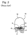
- a light emitting diode 10 which has three light emitting element chips mounted thereon and mixes multiple colors to produce a desired color of light, as shown in Fig. 2.
- This light emitting diode 10 comprises three light emitting element chips 12, 13, 14 mounted on a base 11 that emit light in red, blue and green, respectively, electrode terminals 15, 16, 17 connected to the light emitting element chips 12, 13, 14, respectively, and a bullet-shaped resin sealing member 18 covering the light emitting element chips 12, 13, 14 from above.
- the light emitting diode 10 of this construction can produce light of almost any color by combining the three light emitting element chips 12, 13, 14 that emit light in red, blue and green (see Masakazu Matsumoto, "Electronic Display,” from Ohmsha Co., Ltd., p213, Figs. 6 & 20, July 7, 1995).
- the light emitting diodes 1, 10 described above also have a problem of a large current consumption resulting from the need to make a plurality of light emitting element chips produce light simultaneously.
- An object of the present invention is to provide a light emitting diode capable of producing a variety of intermediate colors of light with a single light emitting element chip.
- Another object of the present invention is to provide a small, inexpensive light emitting diode.
- Still another object of the present invention is to provide a light emitting diode which consumes a small amount of current in the light emitting element chip and which has no need to control the current.
- the present invention provides a light emitting diode which comprises: a substrate; a light emitting element chip mounted on the substrate; a wavelength conversion material to receive light from the light emitting element chip and change wavelengths of the received light; and a wavelength absorbing material to receive the light from the light emitting element chip and the wavelength conversion material and absorb a part of the wavelengths of the received light.
- the substrate is formed with electrodes, which are connected to the light emitting element chip.
- the wavelength conversion material is made from, for example, fluorescent particles and the wavelength absorbing material is made from, for example, coloring particles.
- the wavelength conversion material and the wavelength absorbing material be dispersed in a scatteringly distributed condition in a cover member enclosing the light emitting element chip.
- the cover member may be made from a light transmitting resin material.
- the resin material is mixed with the fluorescent particles for producing light with a wider range of wavelength and with coloring particles for absorbing a desired wavelength range, it is possible to produce a soft, intermediate, pastel color of light based only on the color of light emitted by a single light emitting element chip.
- the fluorescent particles are made from yttrium aluminum garnet (YAG).
- this invention uses yttrium aluminum garnet (YAG) for the fluorescent particles, a wide range of wavelengths, 400 nm to 700 nm, can be produced stably and efficiently by exciting the fluorescent particles.
- YAG yttrium aluminum garnet
- the coloring particles are made from a dye which absorbs a part of wavelengths of light from the light emitting element chip and a part of wavelengths of light that were changed by the fluorescent particles.
- this invention uses a dye for the coloring particles, it is possible to produce a soft, intermediate, pastel color of light with low cost.
- the light emitting element chip is a blue light emitting diode element formed of a gallium nitride compound semiconductor.
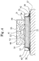
- FIG. 3 to Fig. 5 represent the first embodiment of the invention which is implemented as a surface mount type light emitting diode.
- a surface mount type light emitting diode 31 of this embodiment has a rectangular substrate 32, a pair of electrodes (a cathode electrode 33 and an anode electrode 34) patterned on the substrate 32, and a light emitting element chip 41 arranged almost at a center on the upper surface of the substrate 32.
- the light emitting diode 31 is surface-mounted on a mother board 37 by having its electrodes 33, 34 soldered at 40 on the underside to printed wires 38, 39 (see Fig. 4).
- the light emitting element chip 41 is secured to the substrate 32 by a bonding agent 51 applied to the underside thereof.
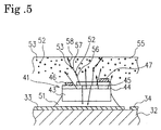
- the light emitting element chip 41 is a blue light emitting element made of a gallium nitride compound semiconductor which is grown by diffusing an n-type semiconductor 44 and a p-type semiconductor 45 over the upper surface of an element substrate 43 of sapphire glass, as shown in Fig. 5.
- the n-type semiconductor 44 and the p-type semiconductor 45 have an n-type electrode 46 and a p-type electrode 47, respectively, which are connected through bonding wires 48, 49 to the cathode electrode 33 and the anode electrode 34, respectively, provided on the substrate 32. Supplying a predetermined amount of current causes the light emitting element chip 41 to emit light in blue.
- This invention is characterized by a wavelength conversion material which, upon receiving light from the light emitting element chip 41, changes the wavelength of the received light and also by a wavelength absorbing material which, upon receiving light from the light emitting element chip and the wavelength conversion material, absorbs a part of the wavelengths of the received light.
- the wavelength conversion material is made from fluorescent particles 52 and the wavelength absorbing material is made from coloring particles 53.
- the fluorescent particles 52 and the coloring particles 53 are preferably scattered in a cover member, for example, a light transmitting resin material 55, which encloses the light emitting element chip 41 and seals and protects the substrate 32.
- the resin material 55 is a transparent base material of silicone resin which is mixed with appropriate amounts of yttrium aluminum garnet (abbreviated YAG), the material for the fluorescent particles 52, and of dye, the material for the coloring particles 53. The added materials are uniformly scattered.
- the resin material 55 containing the fluorescent particles 52 and the coloring particles 53 is formed in a rectangular parallelepiped shape over the upper surface of the substrate 32 except for through-hole portions 35 in the cathode electrode 33 and anode electrode 34.
- the dye used as the coloring particles 53 is made as follows. Appropriate amounts of, for example, four compounds -- phthalocyanine compound, anthraquinone compound, azo compound and quinophthalone compound -- are mixed to generate six colors in advance, i.e., blue, green, yellow, orange, red and violet. In this case, a blue is produced from the phthalocyanine compound, and a green is produced by mixing the phthalocyanine compound and the anthraquinone compound. A yellow is made from the quinophthalone compound, and an orange and a red are produced by mixing the anthraquinone compound and the azo compound.
- a violet is made either by using the anthraquinone compound or by mixing the phthalocyanine compound, anthraquinone compound and azo compound. In this embodiment, these six colors produced in this manner in advance are further mixed to generate a desired chromaticity.
- the coloring particles 53 are not limited to the above-described dye but a pigment may also be used.
- blue light is produced at a boundary plane between the n-type semiconductor 44 and the p-type semiconductor 45.
- the blue light is emitted as blue rays of light 56 in various directions, upward, sideways and downward.
- the blue rays 56 emitted upward in particular excite the fluorescent particles 52 scattered in the resin material 55 to produce wavelength-changed yellow rays 57 with a wider range of wavelength which in turn propagate through the resin material 55 in all directions.
- any intermediate color of rays 58 can be formed by appropriately selecting the kind and amount of a dye, the material for the coloring particles 53 scatteringly distributed in the resin material 55.
- the brightness of an intermediate color can be adjusted by controlling the current flowing through the light emitting element chip 41.
- Fig. 6 is a CIE chromaticity diagram showing a result of chromaticity measurement when various intermediate colors of rays 58 are produced by the light emitting diode 31.
- the diagram has found that although the color of light produced varies depending on the kind of the coloring particles 53 used, many rays are observed in an intermediate color range and few rays light up in those areas on or around the lines connecting the red LED, blue LED and green LED which are close to primary colors.
- Fig. 7 shows a light emitting diode according to the second embodiment of the invention.
- the bonding agent 51 that bonds the light emitting element chip 41 to the substrate 32 is also mixed with the fluorescent particles 52 to form a fluorescent bonding layer 60 so that the rays of light propagating downward from the light emitting element chip 41 can also be changed in wavelength, thereby producing a brighter intermediate color of light. Since other constitutional elements are similar to those of the first embodiment shown in Figs. 3 to 5, their detailed explanations are omitted.
- the blue rays 56 propagating downward from the light emitting element chip 41 excite the fluorescent particles 52 distributed in the fluorescent bonding layer 60 and at the same time the blue rays 56 propagating upward from the light emitting element chip 41 excite the fluorescent particles 52 mixed in the resin material 55, thus producing brighter yellow rays 57.
- the amount of rays of an intermediate color 58 produced by the emitted light passing through the coloring particles 53 increases, the brightness of the intermediate color also increases.
- a current flows through the light emitting element chip 41 blue light is produced at the boundary plane between the n-type semiconductor 44 and the p-type semiconductor 45.
- the blue light is emitted as blue rays of light 56 in various directions, upward, sideways and downward.
- the blue rays 56 emitted downward in particular excite the fluorescent particles 52 scatteringly distributed in the fluorescent bonding layer 60 to produce wavelength-changed yellow rays 57 which in turn propagate in all directions.
- the yellow rays 57 and the blue rays 56 are absorbed by the coloring particles 53 distributed in the resin material 55, thus producing a desired intermediate color of light 58.
- a desired intermediate color of light 58 can be obtained by selecting an appropriate kind and amount of a dye, the material for the coloring particles 53 contained in the resin material 55. Controlling the current applied to the light emitting element chip 41 can adjust the brightness of the light produced.
- a chip type light emitting diode directly surface-mounted on the printed wires 38, 39 provided on the upper surface of the mother board 37 as shown in Fig. 4.
- the light emitting diode according to this invention can also be applied to a lead frame type light emitting diode. That is, a desired intermediate color of light can be produced by rigidly mounting a blue light emitting element chip of gallium nitride compound semiconductor on a base and scatteringly distributing appropriate amounts of the fluorescent particles 52 and the coloring particles 53 in a bullet-shaped resin sealing member.
- the present invention is not limited to this method of connection but also includes other connection methods such as flip-chip mounting using solder bumps.
- the present invention can provide a light emitting diode that can emit an intermediate color of light with a single light emitting element chip. Further, by adjusting a volume ratio between the fluorescent particles and the coloring particles scatteringly distributed in the resin material, the range of wavelength to be absorbed and the amount of wavelength absorption can be changed, thus producing a variety of intermediate colors of light.
- the size of the light emitting diode can be reduced.
- the color of light emitted by the light emitting diode can be selected by the fluorescent particles and coloring particles mixed in the resin material, there is no need to control the current applied to the light emitting element chip, as is required by the conventional light emitting diode.
- the light emitting diode according to the present invention is advantageously used as a chip type light emitting diode for emitting an intermediate color of light and also has a structure suited for mass production.
Landscapes
- Led Device Packages (AREA)
- Led Devices (AREA)
- Luminescent Compositions (AREA)
Applications Claiming Priority (2)
| Application Number | Priority Date | Filing Date | Title |
|---|---|---|---|
| JP2000298579 | 2000-09-29 | ||
| JP2000298579A JP3609709B2 (ja) | 2000-09-29 | 2000-09-29 | 発光ダイオード |
Publications (2)
| Publication Number | Publication Date |
|---|---|
| EP1193772A2 true EP1193772A2 (fr) | 2002-04-03 |
| EP1193772A3 EP1193772A3 (fr) | 2006-03-29 |
Family
ID=18780519
Family Applications (1)
| Application Number | Title | Priority Date | Filing Date |
|---|---|---|---|
| EP01307756A Withdrawn EP1193772A3 (fr) | 2000-09-29 | 2001-09-12 | Diode électroluminescente avec matériaux de conversion et d'absorption de longuer d'onde |
Country Status (7)
| Country | Link |
|---|---|
| US (1) | US6744194B2 (fr) |
| EP (1) | EP1193772A3 (fr) |
| JP (1) | JP3609709B2 (fr) |
| KR (1) | KR100448416B1 (fr) |
| CN (1) | CN1202577C (fr) |
| DE (1) | DE20122795U1 (fr) |
| TW (1) | TWI257712B (fr) |
Cited By (23)
| Publication number | Priority date | Publication date | Assignee | Title |
|---|---|---|---|---|
| DE10361801A1 (de) * | 2003-12-30 | 2005-08-04 | Osram Opto Semiconductors Gmbh | Strahlungsemittierendes und/oder strahlungsempfangendes Halbleiterbauelement und Verfahren zu dessen Herstellung |
| WO2007036206A1 (fr) * | 2005-09-30 | 2007-04-05 | Osram Opto Semiconductors Gmbh | Composant optoelectronique emettant un rayonnement electromagnetique et procede de realisation d'un composant optoelectronique |
| WO2008103876A1 (fr) * | 2007-02-22 | 2008-08-28 | Cree Led Lighting Solutions, Inc. | Dispositifs d'éclairage, procédés d'éclairage, filtres de lumière et procédés de filtrage de lumière |
| WO2009079990A1 (fr) * | 2007-12-21 | 2009-07-02 | Osram Opto Semiconductors Gmbh | Appareil d'éclairage |
| US7564180B2 (en) | 2005-01-10 | 2009-07-21 | Cree, Inc. | Light emission device and method utilizing multiple emitters and multiple phosphors |
| US7666715B2 (en) | 2003-12-30 | 2010-02-23 | Osram Opto Semiconductors Gmbh | Radiation-emitting and/or radiation-receiving semiconductor component and method for the production thereof |
| US7791092B2 (en) | 2003-05-01 | 2010-09-07 | Cree, Inc. | Multiple component solid state white light |
| US7821194B2 (en) | 2006-04-18 | 2010-10-26 | Cree, Inc. | Solid state lighting devices including light mixtures |
| US7967652B2 (en) | 2009-02-19 | 2011-06-28 | Cree, Inc. | Methods for combining light emitting devices in a package and packages including combined light emitting devices |
| US8125137B2 (en) | 2005-01-10 | 2012-02-28 | Cree, Inc. | Multi-chip light emitting device lamps for providing high-CRI warm white light and light fixtures including the same |
| US8333631B2 (en) | 2009-02-19 | 2012-12-18 | Cree, Inc. | Methods for combining light emitting devices in a package and packages including combined light emitting devices |
| US8350461B2 (en) | 2008-03-28 | 2013-01-08 | Cree, Inc. | Apparatus and methods for combining light emitters |
| US8378366B2 (en) | 2007-03-30 | 2013-02-19 | Osram Opto Semiconductors Gmbh | Electromagnetic radiation emitting optoelectronic component and method for manufacturing an optoelectronic component |
| US8556469B2 (en) | 2010-12-06 | 2013-10-15 | Cree, Inc. | High efficiency total internal reflection optic for solid state lighting luminaires |
| US8684559B2 (en) | 2010-06-04 | 2014-04-01 | Cree, Inc. | Solid state light source emitting warm light with high CRI |
| US8998444B2 (en) | 2006-04-18 | 2015-04-07 | Cree, Inc. | Solid state lighting devices including light mixtures |
| US9054282B2 (en) | 2007-08-07 | 2015-06-09 | Cree, Inc. | Semiconductor light emitting devices with applied wavelength conversion materials and methods for forming the same |
| US9084328B2 (en) | 2006-12-01 | 2015-07-14 | Cree, Inc. | Lighting device and lighting method |
| US9435493B2 (en) | 2009-10-27 | 2016-09-06 | Cree, Inc. | Hybrid reflector system for lighting device |
| US10018346B2 (en) | 2006-04-18 | 2018-07-10 | Cree, Inc. | Lighting device and lighting method |
| US10030824B2 (en) | 2007-05-08 | 2018-07-24 | Cree, Inc. | Lighting device and lighting method |
| US10615324B2 (en) | 2013-06-14 | 2020-04-07 | Cree Huizhou Solid State Lighting Company Limited | Tiny 6 pin side view surface mount LED |
| US11251164B2 (en) | 2011-02-16 | 2022-02-15 | Creeled, Inc. | Multi-layer conversion material for down conversion in solid state lighting |
Families Citing this family (59)
| Publication number | Priority date | Publication date | Assignee | Title |
|---|---|---|---|---|
| JP2002190622A (ja) * | 2000-12-22 | 2002-07-05 | Sanken Electric Co Ltd | 発光ダイオード用透光性蛍光カバー |
| KR20030060281A (ko) * | 2002-01-08 | 2003-07-16 | 주식회사 이츠웰 | 발광 다이오드 장치 및 이를 이용한 디스플레이 |
| KR100567548B1 (ko) * | 2002-04-22 | 2006-04-05 | 서울반도체 주식회사 | 백색 칩 발광 다이오드 및 그 제조 방법 |
| JP4360788B2 (ja) * | 2002-08-29 | 2009-11-11 | シチズン電子株式会社 | 液晶表示板用のバックライト及びそれに用いる発光ダイオードの製造方法 |
| JP3782411B2 (ja) * | 2002-09-02 | 2006-06-07 | 松下電器産業株式会社 | 発光装置 |
| US7078737B2 (en) | 2002-09-02 | 2006-07-18 | Matsushita Electric Industrial Co., Ltd. | Light-emitting device |
| JP4185352B2 (ja) * | 2002-11-13 | 2008-11-26 | シチズン電子株式会社 | 発光ダイオード及びその製造方法 |
| JP2005353802A (ja) * | 2004-06-10 | 2005-12-22 | Citizen Electronics Co Ltd | 発光ダイオード |
| US20060006366A1 (en) * | 2004-07-06 | 2006-01-12 | Vladimir Abramov | Wave length shifting compositions for white emitting diode systems |
| US20060044806A1 (en) * | 2004-08-25 | 2006-03-02 | Abramov Vladimir S | Light emitting diode system packages |
| JP2006073950A (ja) * | 2004-09-06 | 2006-03-16 | Kansai Electric Power Co Inc:The | 高耐熱半導体装置 |
| KR20060023443A (ko) * | 2004-09-09 | 2006-03-14 | 이희목 | 발광 장치 |
| DE602005023891D1 (de) * | 2004-10-12 | 2010-11-11 | Philips Intellectual Property | Elektroluminsezente lichtquelle |
| CN100511736C (zh) * | 2005-11-11 | 2009-07-08 | 亿镫光电科技股份有限公司 | 增光发光装置 |
| EP2372223A3 (fr) | 2005-12-21 | 2012-08-01 | Cree, Inc. | Dispositif d'éclairage et procédé d'éclairage |
| EP1963743B1 (fr) | 2005-12-21 | 2016-09-07 | Cree, Inc. | Dispositif d'eclairage |
| EP1969633B1 (fr) | 2005-12-22 | 2018-08-29 | Cree, Inc. | Dispositif d' eclairage |
| JP2007173673A (ja) * | 2005-12-26 | 2007-07-05 | Okaya Electric Ind Co Ltd | カラー発光ダイオード |
| KR100748239B1 (ko) | 2006-02-06 | 2007-08-09 | 삼성전기주식회사 | 발광 다이오드 패키지 및 그 제조방법 |
| US8513875B2 (en) | 2006-04-18 | 2013-08-20 | Cree, Inc. | Lighting device and lighting method |
| KR101517244B1 (ko) | 2006-04-20 | 2015-05-04 | 크리, 인코포레이티드 | 조명 기기 및 조명 방법 |
| US8596819B2 (en) | 2006-05-31 | 2013-12-03 | Cree, Inc. | Lighting device and method of lighting |
| US8029155B2 (en) | 2006-11-07 | 2011-10-04 | Cree, Inc. | Lighting device and lighting method |
| JP5367218B2 (ja) | 2006-11-24 | 2013-12-11 | シャープ株式会社 | 蛍光体の製造方法および発光装置の製造方法 |
| US9441793B2 (en) | 2006-12-01 | 2016-09-13 | Cree, Inc. | High efficiency lighting device including one or more solid state light emitters, and method of lighting |
| EP2089654B1 (fr) | 2006-12-07 | 2016-08-03 | Cree, Inc. | Dispositif et procédé d'éclairage |
| KR20100020464A (ko) | 2007-05-08 | 2010-02-22 | 크리 엘이디 라이팅 솔루션즈, 인크. | 조명 장치 및 조명 방법 |
| KR101460832B1 (ko) | 2007-05-08 | 2014-11-12 | 크리, 인코포레이티드 | 조명 장치 및 조명 방법 |
| TWI422785B (zh) | 2007-05-08 | 2014-01-11 | 克里公司 | 照明裝置及照明方法 |
| US7901107B2 (en) | 2007-05-08 | 2011-03-08 | Cree, Inc. | Lighting device and lighting method |
| WO2009008250A1 (fr) | 2007-07-09 | 2009-01-15 | Sharp Kabushiki Kaisha | Groupe de particules de matière luminescente et dispositif émettant de la lumière utilisant celles-ci |
| KR101722265B1 (ko) | 2007-10-10 | 2017-03-31 | 크리, 인코포레이티드 | 조명 장치 및 그 제조 방법 |
| JP2009239116A (ja) * | 2008-03-27 | 2009-10-15 | Sharp Corp | 発光装置 |
| JP2009252898A (ja) * | 2008-04-03 | 2009-10-29 | Toyoda Gosei Co Ltd | 光源装置 |
| US8240875B2 (en) | 2008-06-25 | 2012-08-14 | Cree, Inc. | Solid state linear array modules for general illumination |
| CN101330119B (zh) * | 2008-07-22 | 2010-06-02 | 中国科学院长春光学精密机械与物理研究所 | 一种染料激活的绿色发光二极管的制备方法 |
| US20100033091A1 (en) * | 2008-08-08 | 2010-02-11 | Glory Science Co., Ltd. | Light emitting unit and method of manufacturing the light emitting unit |
| JPWO2010116953A1 (ja) * | 2009-04-06 | 2012-10-18 | シャープ株式会社 | 蛍光体粒子群およびそれを用いた発光装置、液晶テレビ |
| JP2010245481A (ja) * | 2009-04-10 | 2010-10-28 | Sharp Corp | 発光装置 |
| US8921876B2 (en) | 2009-06-02 | 2014-12-30 | Cree, Inc. | Lighting devices with discrete lumiphor-bearing regions within or on a surface of remote elements |
| WO2011037877A1 (fr) | 2009-09-25 | 2011-03-31 | Cree, Inc. | Dispositif d'éclairage à faible éblouissement et à grande uniformité du niveau de lumière |
| KR101098006B1 (ko) | 2009-09-29 | 2011-12-23 | 한국화학연구원 | (할로)실리케이트계 형광체 및 이의 제조방법 |
| CN102656248B (zh) | 2010-01-08 | 2014-07-16 | 夏普株式会社 | 荧光体、发光装置及使用它的液晶显示装置 |
| TWI393274B (zh) * | 2010-02-26 | 2013-04-11 | 榮創能源科技股份有限公司 | 發光二極體封裝結構及其製造方法 |
| US9275979B2 (en) | 2010-03-03 | 2016-03-01 | Cree, Inc. | Enhanced color rendering index emitter through phosphor separation |
| US20110291132A1 (en) * | 2010-05-28 | 2011-12-01 | Fang-Chang Liu | Light-emiting device with improved color rendering index |
| US9335531B2 (en) | 2011-12-30 | 2016-05-10 | Cree, Inc. | LED lighting using spectral notching |
| US9435524B2 (en) | 2011-12-30 | 2016-09-06 | Cree, Inc. | Liquid cooled LED systems |
| US9482421B2 (en) | 2011-12-30 | 2016-11-01 | Cree, Inc. | Lamp with LED array and thermal coupling medium |
| US9685594B2 (en) | 2012-05-31 | 2017-06-20 | Panasonic Intellectual Property Management Co., Ltd. | LED module and method of preparing the LED module, lighting device |
| US9960322B2 (en) | 2014-04-23 | 2018-05-01 | Cree, Inc. | Solid state lighting devices incorporating notch filtering materials |
| EP3274423B1 (fr) * | 2015-03-24 | 2019-09-18 | Koninklijke Philips N.V. | Del convertie luminophore émettant dans le bleu avec pigment bleu |
| KR101639992B1 (ko) | 2015-06-04 | 2016-07-15 | 한국화학연구원 | 알칼리토금속 실리케이트를 이용한 산질화물계 형광체의 제조방법 |
| JP6632834B2 (ja) | 2015-08-24 | 2020-01-22 | スタンレー電気株式会社 | 発光装置 |
| US10260683B2 (en) | 2017-05-10 | 2019-04-16 | Cree, Inc. | Solid-state lamp with LED filaments having different CCT's |
| KR102452484B1 (ko) | 2017-08-11 | 2022-10-11 | 삼성전자주식회사 | 발광소자 패키지 및 발광소자 패키지 모듈 |
| KR102049524B1 (ko) | 2018-03-08 | 2020-01-08 | 주식회사 한국공업엔지니어링 | 와전류탐상검사를 이용하여 튜브 확관부의 결함 측정을 위한 대비시험편 및 이를 이용한 결함측정방법 |
| CN112526784A (zh) * | 2019-09-19 | 2021-03-19 | 李崇华 | 发光二极管装置及包含其之背光模块与显示设备 |
| CN114188456A (zh) * | 2020-09-14 | 2022-03-15 | 李崇华 | 白光发光二极管及其背光模块与显示设备 |
Family Cites Families (15)
| Publication number | Priority date | Publication date | Assignee | Title |
|---|---|---|---|---|
| DE19638667C2 (de) * | 1996-09-20 | 2001-05-17 | Osram Opto Semiconductors Gmbh | Mischfarbiges Licht abstrahlendes Halbleiterbauelement mit Lumineszenzkonversionselement |
| DE29724847U1 (de) * | 1996-06-26 | 2004-09-30 | Osram Opto Semiconductors Gmbh | Lichtabstrahlendes Halbleiterbauelement mit Lumineszenzkonversionselement |
| TW383508B (en) * | 1996-07-29 | 2000-03-01 | Nichia Kagaku Kogyo Kk | Light emitting device and display |
| JP3065544B2 (ja) * | 1996-12-06 | 2000-07-17 | スタンレー電気株式会社 | 蛍光剤入りledランプ |
| US5895932A (en) * | 1997-01-24 | 1999-04-20 | International Business Machines Corporation | Hybrid organic-inorganic semiconductor light emitting diodes |
| JP2998696B2 (ja) * | 1997-05-17 | 2000-01-11 | 日亜化学工業株式会社 | 発光ダイオード |
| JP3327170B2 (ja) * | 1997-05-17 | 2002-09-24 | 日亜化学工業株式会社 | 発光ダイオードの製造方法 |
| US5813753A (en) * | 1997-05-27 | 1998-09-29 | Philips Electronics North America Corporation | UV/blue led-phosphor device with efficient conversion of UV/blues light to visible light |
| JP4271747B2 (ja) * | 1997-07-07 | 2009-06-03 | 株式会社朝日ラバー | 発光ダイオード用透光性被覆材及び蛍光カラー光源 |
| US5847507A (en) * | 1997-07-14 | 1998-12-08 | Hewlett-Packard Company | Fluorescent dye added to epoxy of light emitting diode lens |
| JPH11145519A (ja) * | 1997-09-02 | 1999-05-28 | Toshiba Corp | 半導体発光素子、半導体発光装置および画像表示装置 |
| KR20000007067A (ko) * | 1999-11-23 | 2000-02-07 | 김창태 | 형광물질을 가진 엘이디 패키지 제조방법 |
| KR200181326Y1 (ko) * | 1999-12-24 | 2000-05-15 | 서울반도체주식회사 | 색변환 발광다이오드 |
| JP3809760B2 (ja) * | 2000-02-18 | 2006-08-16 | 日亜化学工業株式会社 | 発光ダイオード |
| KR200205427Y1 (ko) * | 2000-05-10 | 2000-12-01 | 이정훈 | 파장 변환 발광 다이오드 |
-
2000
- 2000-09-29 JP JP2000298579A patent/JP3609709B2/ja not_active Expired - Lifetime
-
2001
- 2001-09-12 EP EP01307756A patent/EP1193772A3/fr not_active Withdrawn
- 2001-09-12 TW TW090122637A patent/TWI257712B/zh not_active IP Right Cessation
- 2001-09-12 DE DE20122795U patent/DE20122795U1/de not_active Expired - Lifetime
- 2001-09-17 US US09/953,302 patent/US6744194B2/en not_active Expired - Lifetime
- 2001-09-17 KR KR10-2001-0057106A patent/KR100448416B1/ko not_active Expired - Fee Related
- 2001-09-28 CN CNB011412135A patent/CN1202577C/zh not_active Expired - Lifetime
Cited By (32)
| Publication number | Priority date | Publication date | Assignee | Title |
|---|---|---|---|---|
| US8901585B2 (en) | 2003-05-01 | 2014-12-02 | Cree, Inc. | Multiple component solid state white light |
| US7791092B2 (en) | 2003-05-01 | 2010-09-07 | Cree, Inc. | Multiple component solid state white light |
| DE10361801A1 (de) * | 2003-12-30 | 2005-08-04 | Osram Opto Semiconductors Gmbh | Strahlungsemittierendes und/oder strahlungsempfangendes Halbleiterbauelement und Verfahren zu dessen Herstellung |
| US7666715B2 (en) | 2003-12-30 | 2010-02-23 | Osram Opto Semiconductors Gmbh | Radiation-emitting and/or radiation-receiving semiconductor component and method for the production thereof |
| US7564180B2 (en) | 2005-01-10 | 2009-07-21 | Cree, Inc. | Light emission device and method utilizing multiple emitters and multiple phosphors |
| US8513873B2 (en) | 2005-01-10 | 2013-08-20 | Cree, Inc. | Light emission device |
| US8410680B2 (en) | 2005-01-10 | 2013-04-02 | Cree, Inc. | Multi-chip light emitting device lamps for providing high-CRI warm white light and light fixtures including the same |
| US8125137B2 (en) | 2005-01-10 | 2012-02-28 | Cree, Inc. | Multi-chip light emitting device lamps for providing high-CRI warm white light and light fixtures including the same |
| WO2007036206A1 (fr) * | 2005-09-30 | 2007-04-05 | Osram Opto Semiconductors Gmbh | Composant optoelectronique emettant un rayonnement electromagnetique et procede de realisation d'un composant optoelectronique |
| US8476655B2 (en) | 2005-09-30 | 2013-07-02 | Osram Opto Semiconductors Gmbh | Electromagnetic-radiation-emitting optoelectronic component and method for producing an optoelectronic component |
| US10018346B2 (en) | 2006-04-18 | 2018-07-10 | Cree, Inc. | Lighting device and lighting method |
| US8212466B2 (en) | 2006-04-18 | 2012-07-03 | Cree, Inc. | Solid state lighting devices including light mixtures |
| US7821194B2 (en) | 2006-04-18 | 2010-10-26 | Cree, Inc. | Solid state lighting devices including light mixtures |
| US8998444B2 (en) | 2006-04-18 | 2015-04-07 | Cree, Inc. | Solid state lighting devices including light mixtures |
| US9084328B2 (en) | 2006-12-01 | 2015-07-14 | Cree, Inc. | Lighting device and lighting method |
| US8506114B2 (en) | 2007-02-22 | 2013-08-13 | Cree, Inc. | Lighting devices, methods of lighting, light filters and methods of filtering light |
| WO2008103876A1 (fr) * | 2007-02-22 | 2008-08-28 | Cree Led Lighting Solutions, Inc. | Dispositifs d'éclairage, procédés d'éclairage, filtres de lumière et procédés de filtrage de lumière |
| US8378366B2 (en) | 2007-03-30 | 2013-02-19 | Osram Opto Semiconductors Gmbh | Electromagnetic radiation emitting optoelectronic component and method for manufacturing an optoelectronic component |
| US10030824B2 (en) | 2007-05-08 | 2018-07-24 | Cree, Inc. | Lighting device and lighting method |
| US9054282B2 (en) | 2007-08-07 | 2015-06-09 | Cree, Inc. | Semiconductor light emitting devices with applied wavelength conversion materials and methods for forming the same |
| US8716729B2 (en) | 2007-12-21 | 2014-05-06 | Osram Opto Semiconductors Gmbh | Lighting device |
| WO2009079990A1 (fr) * | 2007-12-21 | 2009-07-02 | Osram Opto Semiconductors Gmbh | Appareil d'éclairage |
| US8513871B2 (en) | 2008-03-28 | 2013-08-20 | Cree, Inc. | Apparatus and methods for combining light emitters |
| US8350461B2 (en) | 2008-03-28 | 2013-01-08 | Cree, Inc. | Apparatus and methods for combining light emitters |
| US8333631B2 (en) | 2009-02-19 | 2012-12-18 | Cree, Inc. | Methods for combining light emitting devices in a package and packages including combined light emitting devices |
| US7967652B2 (en) | 2009-02-19 | 2011-06-28 | Cree, Inc. | Methods for combining light emitting devices in a package and packages including combined light emitting devices |
| US9435493B2 (en) | 2009-10-27 | 2016-09-06 | Cree, Inc. | Hybrid reflector system for lighting device |
| US8684559B2 (en) | 2010-06-04 | 2014-04-01 | Cree, Inc. | Solid state light source emitting warm light with high CRI |
| US9599291B2 (en) | 2010-06-04 | 2017-03-21 | Cree, Inc. | Solid state light source emitting warm light with high CRI |
| US8556469B2 (en) | 2010-12-06 | 2013-10-15 | Cree, Inc. | High efficiency total internal reflection optic for solid state lighting luminaires |
| US11251164B2 (en) | 2011-02-16 | 2022-02-15 | Creeled, Inc. | Multi-layer conversion material for down conversion in solid state lighting |
| US10615324B2 (en) | 2013-06-14 | 2020-04-07 | Cree Huizhou Solid State Lighting Company Limited | Tiny 6 pin side view surface mount LED |
Also Published As
| Publication number | Publication date |
|---|---|
| US6744194B2 (en) | 2004-06-01 |
| US20020039002A1 (en) | 2002-04-04 |
| JP2002111073A (ja) | 2002-04-12 |
| CN1345098A (zh) | 2002-04-17 |
| KR100448416B1 (ko) | 2004-09-13 |
| CN1202577C (zh) | 2005-05-18 |
| DE20122795U1 (de) | 2007-12-27 |
| EP1193772A3 (fr) | 2006-03-29 |
| KR20020025696A (ko) | 2002-04-04 |
| JP3609709B2 (ja) | 2005-01-12 |
| TWI257712B (en) | 2006-07-01 |
Similar Documents
| Publication | Publication Date | Title |
|---|---|---|
| US6744194B2 (en) | Light emitting diode | |
| US6914267B2 (en) | Light emitting diode | |
| US8598608B2 (en) | Light emitting device | |
| US7759683B2 (en) | White light emitting diode | |
| KR100872295B1 (ko) | 백색 발광장치 및 이를 이용한 백색 광원 모듈 | |
| US7781783B2 (en) | White light LED device | |
| CN100411202C (zh) | 白光发光二极管 | |
| JP2000294834A (ja) | 半導体発光装置 | |
| JP3400958B2 (ja) | 多色発光ダイオード | |
| JP2000349345A (ja) | 半導体発光装置 | |
| JP2001135861A (ja) | 半導体発光装置及びその製造方法 | |
| JP2001177157A (ja) | 半導体発光装置 | |
| CN102779814A (zh) | 可发出白光的发光元件及其混光方法 | |
| KR101195430B1 (ko) | 백색 발광장치 및 이를 이용한 백색 광원 모듈 | |
| US20080297702A1 (en) | Light Emitting Diode Package and Driving Method Thereof | |
| JP2008034665A (ja) | 発光装置及びその製造方法 | |
| KR100990647B1 (ko) | 백색 발광장치 및 이를 이용한 백색 광원 모듈 | |
| KR20130027653A (ko) | Led 백색 광원모듈 | |
| KR200402110Y1 (ko) | 발광 다이오드 구조 | |
| CN107561773A (zh) | 一种高色域led、背光模组和显示设备 | |
| KR200421146Y1 (ko) | 발광장치 | |
| US20070296330A1 (en) | Module composed of two light sources and generating tri-band white light with adjustable chromaticity diagram | |
| JPH11204836A (ja) | 半導体発光素子 |
Legal Events
| Date | Code | Title | Description |
|---|---|---|---|
| PUAI | Public reference made under article 153(3) epc to a published international application that has entered the european phase |
Free format text: ORIGINAL CODE: 0009012 |
|
| AK | Designated contracting states |
Kind code of ref document: A2 Designated state(s): AT BE CH CY DE DK ES FI FR GB GR IE IT LI LU MC NL PT SE TR |
|
| AX | Request for extension of the european patent |
Free format text: AL;LT;LV;MK;RO;SI |
|
| PUAL | Search report despatched |
Free format text: ORIGINAL CODE: 0009013 |
|
| AK | Designated contracting states |
Kind code of ref document: A3 Designated state(s): AT BE CH CY DE DK ES FI FR GB GR IE IT LI LU MC NL PT SE TR |
|
| AX | Request for extension of the european patent |
Extension state: AL LT LV MK RO SI |
|
| 17P | Request for examination filed |
Effective date: 20060823 |
|
| 17Q | First examination report despatched |
Effective date: 20061011 |
|
| AKX | Designation fees paid |
Designated state(s): DE |
|
| 17Q | First examination report despatched |
Effective date: 20061011 |
|
| STAA | Information on the status of an ep patent application or granted ep patent |
Free format text: STATUS: THE APPLICATION IS DEEMED TO BE WITHDRAWN |
|
| 18D | Application deemed to be withdrawn |
Effective date: 20071010 |