EP1196790B1 - Gerät und verfahren zur temperaturkontrolle von integrierten schaltungen während der prüfung - Google Patents
Gerät und verfahren zur temperaturkontrolle von integrierten schaltungen während der prüfung Download PDFInfo
- Publication number
- EP1196790B1 EP1196790B1 EP00947340A EP00947340A EP1196790B1 EP 1196790 B1 EP1196790 B1 EP 1196790B1 EP 00947340 A EP00947340 A EP 00947340A EP 00947340 A EP00947340 A EP 00947340A EP 1196790 B1 EP1196790 B1 EP 1196790B1
- Authority
- EP
- European Patent Office
- Prior art keywords
- temperature
- devices
- integrated circuit
- chuck
- circuit devices
- Prior art date
- Legal status (The legal status is an assumption and is not a legal conclusion. Google has not performed a legal analysis and makes no representation as to the accuracy of the status listed.)
- Expired - Lifetime
Links
- 238000012360 testing method Methods 0.000 title claims abstract description 75
- 238000000034 method Methods 0.000 title claims description 37
- 238000010438 heat treatment Methods 0.000 claims abstract description 85
- 239000012530 fluid Substances 0.000 claims abstract description 25
- 230000001276 controlling effect Effects 0.000 claims description 13
- 238000001816 cooling Methods 0.000 claims description 13
- 230000001105 regulatory effect Effects 0.000 claims description 5
- 235000012431 wafers Nutrition 0.000 description 64
- 239000007788 liquid Substances 0.000 description 28
- 238000010586 diagram Methods 0.000 description 11
- 238000004519 manufacturing process Methods 0.000 description 7
- 230000003134 recirculating effect Effects 0.000 description 7
- 238000013459 approach Methods 0.000 description 6
- 230000000694 effects Effects 0.000 description 6
- 238000012544 monitoring process Methods 0.000 description 5
- 238000013021 overheating Methods 0.000 description 4
- 230000008569 process Effects 0.000 description 4
- 230000006641 stabilisation Effects 0.000 description 4
- GQIUQDDJKHLHTB-UHFFFAOYSA-N trichloro(ethenyl)silane Chemical compound Cl[Si](Cl)(Cl)C=C GQIUQDDJKHLHTB-UHFFFAOYSA-N 0.000 description 4
- OKKJLVBELUTLKV-UHFFFAOYSA-N Methanol Chemical compound OC OKKJLVBELUTLKV-UHFFFAOYSA-N 0.000 description 3
- 239000003570 air Substances 0.000 description 3
- 238000006243 chemical reaction Methods 0.000 description 3
- 239000007789 gas Substances 0.000 description 3
- 238000012545 processing Methods 0.000 description 3
- 230000004044 response Effects 0.000 description 3
- 239000004065 semiconductor Substances 0.000 description 3
- LYCAIKOWRPUZTN-UHFFFAOYSA-N Ethylene glycol Chemical compound OCCO LYCAIKOWRPUZTN-UHFFFAOYSA-N 0.000 description 2
- 230000008901 benefit Effects 0.000 description 2
- 239000002826 coolant Substances 0.000 description 2
- PMHQVHHXPFUNSP-UHFFFAOYSA-M copper(1+);methylsulfanylmethane;bromide Chemical compound Br[Cu].CSC PMHQVHHXPFUNSP-UHFFFAOYSA-M 0.000 description 2
- 238000013461 design Methods 0.000 description 2
- 238000003745 diagnosis Methods 0.000 description 2
- 230000009977 dual effect Effects 0.000 description 2
- 238000005516 engineering process Methods 0.000 description 2
- 230000014759 maintenance of location Effects 0.000 description 2
- 239000000758 substrate Substances 0.000 description 2
- 238000012546 transfer Methods 0.000 description 2
- XLYOFNOQVPJJNP-UHFFFAOYSA-N water Substances O XLYOFNOQVPJJNP-UHFFFAOYSA-N 0.000 description 2
- DFUYAWQUODQGFF-UHFFFAOYSA-N 1-ethoxy-1,1,2,2,3,3,4,4,4-nonafluorobutane Chemical compound CCOC(F)(F)C(F)(F)C(F)(F)C(F)(F)F DFUYAWQUODQGFF-UHFFFAOYSA-N 0.000 description 1
- SQEGLLMNIBLLNQ-UHFFFAOYSA-N 1-ethoxy-1,1,2,3,3,3-hexafluoro-2-(trifluoromethyl)propane Chemical compound CCOC(F)(F)C(F)(C(F)(F)F)C(F)(F)F SQEGLLMNIBLLNQ-UHFFFAOYSA-N 0.000 description 1
- XUIMIQQOPSSXEZ-UHFFFAOYSA-N Silicon Chemical compound [Si] XUIMIQQOPSSXEZ-UHFFFAOYSA-N 0.000 description 1
- WYTGDNHDOZPMIW-RCBQFDQVSA-N alstonine Natural products C1=CC2=C3C=CC=CC3=NC2=C2N1C[C@H]1[C@H](C)OC=C(C(=O)OC)[C@H]1C2 WYTGDNHDOZPMIW-RCBQFDQVSA-N 0.000 description 1
- 239000012080 ambient air Substances 0.000 description 1
- 230000003466 anti-cipated effect Effects 0.000 description 1
- 230000008859 change Effects 0.000 description 1
- 230000003750 conditioning effect Effects 0.000 description 1
- 239000004035 construction material Substances 0.000 description 1
- 239000012809 cooling fluid Substances 0.000 description 1
- 239000000110 cooling liquid Substances 0.000 description 1
- 230000003247 decreasing effect Effects 0.000 description 1
- 238000005485 electric heating Methods 0.000 description 1
- 230000017525 heat dissipation Effects 0.000 description 1
- WGCNASOHLSPBMP-UHFFFAOYSA-N hydroxyacetaldehyde Natural products OCC=O WGCNASOHLSPBMP-UHFFFAOYSA-N 0.000 description 1
- 230000003116 impacting effect Effects 0.000 description 1
- 230000006872 improvement Effects 0.000 description 1
- 238000009413 insulation Methods 0.000 description 1
- 239000000463 material Substances 0.000 description 1
- 230000007246 mechanism Effects 0.000 description 1
- 239000000203 mixture Substances 0.000 description 1
- 238000004806 packaging method and process Methods 0.000 description 1
- 230000000717 retained effect Effects 0.000 description 1
- 230000035945 sensitivity Effects 0.000 description 1
- 238000000926 separation method Methods 0.000 description 1
- 229910052710 silicon Inorganic materials 0.000 description 1
- 239000010703 silicon Substances 0.000 description 1
Images





Classifications
-
- G—PHYSICS
- G01—MEASURING; TESTING
- G01R—MEASURING ELECTRIC VARIABLES; MEASURING MAGNETIC VARIABLES
- G01R31/00—Arrangements for testing electric properties; Arrangements for locating electric faults; Arrangements for electrical testing characterised by what is being tested not provided for elsewhere
- G01R31/28—Testing of electronic circuits, e.g. by signal tracer
- G01R31/2851—Testing of integrated circuits [IC]
- G01R31/2855—Environmental, reliability or burn-in testing
- G01R31/2872—Environmental, reliability or burn-in testing related to electrical or environmental aspects, e.g. temperature, humidity, vibration, nuclear radiation
- G01R31/2874—Environmental, reliability or burn-in testing related to electrical or environmental aspects, e.g. temperature, humidity, vibration, nuclear radiation related to temperature
-
- G—PHYSICS
- G01—MEASURING; TESTING
- G01R—MEASURING ELECTRIC VARIABLES; MEASURING MAGNETIC VARIABLES
- G01R31/00—Arrangements for testing electric properties; Arrangements for locating electric faults; Arrangements for electrical testing characterised by what is being tested not provided for elsewhere
- G01R31/28—Testing of electronic circuits, e.g. by signal tracer
- G01R31/2851—Testing of integrated circuits [IC]
- G01R31/2886—Features relating to contacting the IC under test, e.g. probe heads; chucks
- G01R31/2891—Features relating to contacting the IC under test, e.g. probe heads; chucks related to sensing or controlling of force, position, temperature
Definitions
- the present invention relates to the temperature control of integrated circuit ("IC") devices during testing.
- the invention relates to apparatus and methods for controlling the temperature of such devices when tested at wafer level.
- Wafer prober interfaces are used as an interface with a test system. In a wafer prober interface, temporary contacts such as needles are placed into electrical contact with pads formed on the device, such as for power and input/output signals. The pads are formed while the device is still part of the wafer, that is, before the wafer is cut into individual or “singulated" devices. A test pattern is then applied via these pads.
- Thermal control of devices during testing has been recognized as an issue in testing of IC devices.
- One particular problem with testing IC devices is that they are tested before temperature control devices such as heat sinks and fans are attached.
- temperature control can be achieved by placing the device in contact with a large thermal mass, which is held at the desired temperature. This method is generally unsatisfactory, however, if the value of the power dissipation of the device varies over a wide range.
- One approach to controlling the temperature of a device under test comprises placing the device in contact with a temperature forcing system.
- the temperature forcing system is used to vary the degree of cooling or heating in order to maintain the device at the desired temperature set point during the test.
- Control of such systems typically uses a feedback loop based on the output of a temperature sensor, which is in contact with the device or, in certain cases, built into the device itself.
- Typical temperature forcing systems often use forced air convection systems that extend well beyond the desired forcing temperature range at both the hot and cold ends. In this way, an attempt can be made to accelerate the device's temperature conditioning by overcooling or overheating. As the nominal power density of the devices continues to increase, the ability of forced air convection systems to overcool reaches practical limits, causing increases in the temperature error between the desired and actual temperatures. Another problem is the increased sensitivity that devices fabricated in the latest processes have to high temperatures. The potential for chip damage due to overheating adds risk to the use of the overheating approach. The combination of the limited ability to overcool and the need to be more conservative by not overheating results in an increased time to reach set point, with lost utilization of expensive test equipment and engineering personnel as the expense.
- the approach used in wafer probing for temperature control is to provide a thermal mass in the form of a heated and/or cooled chuck on which the wafer is placed during testing.
- the chuck attempts to maintain the temperature of the whole wafer at a desired set point during testing.
- An example of such a system is the ThermoChuck available from Temptronic Corp. of Newton, Massachusetts.
- US-A-5,210,485 describes a bum-in wafer test apparatus that heats a plurality of integrated circuit devices on a wafer during testing.
- a heater element is adapted to evenly and controllably heat the individual devices, and comprises a plurality of electrically conductive serpentine traces on a silicon substrate. The number and arrangement of traces corresponds to the number and arrangement of devices on the wafer.
- An alternative bum-in test apparatus is described in EP-A-0,631,149.
- a plurality of semi-conductor chips are heated during testing by placing the individual chips, singularised from a wafer, in a heating assembly having an aperture for each chip.
- Each aperture has its own heating element, the elements being powered by a common power line.
- DE-A-197 00 839 describes an alternative wafer test apparatus, in which a temperature stabilisation device is provided for setting the temperature of a semiconductor wafer to be tested.
- the temperature stabilisation device comprises a first heat stabilisation stage for setting the temperature of the wafer and a second heat stabilisation stage for removing heat dissipated from the first stage.
- the two stages are independently controllable, and preferably have the form of Peltier devices.
- an apparatus for control of integrated circuit devices under test includes a heat exchanger having a surface disposed to contact each of the plurality of integrated circuit devices.
- the surface has a plurality of regions corresponding to respective ones of the plurality of integrated circuit devices.
- the temperature of each of the plurality of integrated circuit devices is individually controlled at each of the plurality of regions.
- the heat exchanger may comprise a chuck having a plurality of heating elements disposed at each of the regions, and the chuck may include a heat sink wherein each of the heating elements regulates the temperature of a corresponding one of the regions at a temperature above a temperature determined by the heat sink.
- the temperature of each region may be individually controlled by a heating element disposed on a heat sink or by a plurality of heating elements disposed over a corresponding one of a plurality of heat sinks.
- the plurality of integrated circuit devices may be formed on a wafer and the surface may be disposed to contact the wafer such that the plurality of regions correspond to respective ones of the plurality of integrated circuit devices formed on the wafer.
- the plurality of integrated circuit devices may be singulated devices, and the surface is disposed to contact the singulated devices such that the plurality of regions correspond to respective ones of the singulated devices.
- the heat exchanger comprises a chuck for locating the devices during testing.
- the apparatus further comprises multiple temperature control devices to individually control the temperature of each of the plurality of integrated circuit devices arranged in the chuck to correspond with the arrangement on the wafer of the devices being tested.
- the chuck may be provided with means for controlling its temperature during the testing, and the means for controlling the chuck temperature may comprise a supply of temperature-controlled fluid or an electrical device.
- the multiple temperature control devices may comprise heating elements, and a heat exchanger body may be provided for each heating element or a single heat exchanger body may be provided for the multiple heating elements.
- a method of controlling the temperature of a plurality of integrated circuit devices during testing includes placing the plurality of integrated circuit device in contact with a respective one of a plurality of regions of a surface of a heat exchanger. The temperature of each of the plurality of integrated circuit devices at each of the plurality of regions is controlled individually.
- the heat exchanger may comprise a chuck having a plurality of heating elements disposed at each of the regions, and the chuck may include a heat sink wherein each of the heating elements regulates the temperature of a corresponding one of the regions at a temperature above a temperature determined by the heat sink.
- the temperature of each region may be individually controlled by a heating element disposed on a heat sink or by a plurality of heating elements disposed over a corresponding one of a plurality of heat sinks.
- the plurality of integrated circuit devices may be formed on a wafer and the surface may be disposed to contact the wafer such that the plurality of regions correspond to respective ones of the plurality of integrated circuit devices formed on the wafer.
- the plurality of integrated circuit devices may be singulated devices, and the surface may be disposed to contact the singulated devices such that the plurality of regions correspond to respective ones of the singulated devices.
- the placing the plurality of integrated circuit devices comprises locating the devices at a test location at which temperature control devices are arranged to correspond with the arrangement of the devices being tested. The individual devices are tested.
- the method may further comprise singulating the devices formed on the wafer before testing, wherein the singulated devices are arranged on the chuck in the same arrangement as when they were formed on the wafer.
- the temperature of each of a plurality of integrated circuit devices may be individually controlled based on the power usage of the integrated circuit devices.
- Fig. 1 illustrates a heat exchanger that provides conductive thermal control of a device 20.
- the heat exchange includes a heat sink 10, which accommodates a circulating cooling liquid 12, a heating element 14, and a closed loop control 16 to hold a contact surface 18, of the test device and a device 20, at a set point temperature.
- the heat exchanger device also includes a power source 22 used by the closed loop control 16 in maintaining the contact surface 18 at the set point temperature.
- the liquid 12 is preferably held at a constant temperature that is sufficiently below the set point temperature, which can be above or below the ambient temperature.
- the heating element 14 is then used to bring the temperature of the contact surface 18 to the desired set point temperature.
- the liquid 12 cools the heating element 14 regardless of whether the set point temperature is above or below the ambient temperature.
- the heat exchanger of Fig. 1 allows the contact surface temperature to be changed rapidly to compensate for variations in an IC device's instantaneous power dissipation. Also, the heating element 14 can be fairly compact, allowing more flexibility to accommodate typical device testing situations.
- the temperature range for the liquid is typically -60°C to +60°C. At any point in this temperature range, the viscosity of the liquid and the resulting flow rate are preferably consistent within some percentage to avoid negatively impacting the thermal control performance.
- One approach to achieve this combination of percentages which may be advantageously used with the apparatus according to the invention is described in commonly assigned U.S. Patent Application Serial No. 09/352,762, entitled “APPARATUS, METHOD AND SYSTEM OF LIQUID-BASED, WIDE RANGE, FAST RESPONSE TEMPERATURE CONTROL OF ELECTRONIC DEVICES", filed on July 14, 1999.
- Fig. 2A is a simplified block diagram of a system such as that shown in Fig. 1.
- a temperature control system 140 controls a heat exchanger 216 which is in thermal contact with a device under test ("DUT") 182.
- the DUT 182 is preferably in physical contact with a surface of the heat exchanger 216.
- a single DUT is shown.
- the present invention allows for temperature control of the DUT 182 to a plurality of integrated circuit devices that may be tested at the same time.
- Figs. 2B and 2C show examples of more specific implementations of the heat exchanger 216 and DUT 182 generally shown in Fig. 2A.
- the heat exchanger 216 comprises a chuck 120 having a heating element 149 in thermal contact with the DUT 182.
- the heat exchanger 216 comprises the heating element 14 and a heat sink 10 whose temperature is regulated with a liquid 12, such as in the manner described in reference to in Fig. 1.
- a heat exchanger 216 comprises a chuck 120 on which a plurality of heating elements 149 are incorporated.
- a plurality of DUTs 182 are located on the heating element 149, preferably in a one-to-one correspondence. This one-to-one correspondence between the heating elements 149 and the DUTs 182 provides the ability to control independently the temperature of each DUT 182 during a test.
- Fig. 8B shows an alternate embodiment in which separate heat exchanger bodies 153 are provided for each of a plurality of heaters 149.
- Each heat exchanger bodies 153 contain a cavity which allows a liquid to flow through them to act as a heat sink in the manner discussed above.
- the heat exchanger bodies 153 may be part of a single chuck 120.
- Fig. 8B shows separate heat exchanger bodies 153 for each heating element 149, these bodies 153 may thermally impact each other depending on the level of thermal insulation between them. The same is true for the heating elements 149 themselves, irrespective of how many heat exchanger bodies 153 are present.
- the individual heating elements 149 may be implemented, for example, as a three layer co-fired aluminum nitride heater substrate with a heater trace between the first two layers and the RTD trace between the last two layers.
- the heater trace provides the heat energy and the RTD trace provides temperature information.
- the two traces are electrically isolated while being at essentially the same thermal position due to the thermal conductivity of the aluminum nitride layers.
- the heating elements 149 are resistive heaters. It is to be understood, however, that many other types of heating elements 149 may be used, including without limitation a heater utilizing lasers, other optics, or electro-magnetic waves.
- FIGs. 10A and 10B are respective perspective and top views of an exemplary heat exchanger in accordance with the invention.
- a chuck 122 serves to locate, that is, align, a whole wafer.
- the chuck 122 is a fluid cooled, incorporating fluid cavity 124, a fluid inlet 126 and fluid outlet 128.
- the inlet 126 and the outlet 128 are connected through fluid supply lines 133 to the temperature control system such as that described above in reference to Fig. 1.
- Disposed on the upper surface of the fluid cooled chuck 122 is an array 129 of heating elements 149, which are connected to the temperature control system via a heater control cable 134.
- Each heating element 149 in the array 129 has a size and shape corresponding to that of the associated IC device to be tested on the wafer and the pattern of heating elements 149 matches that of the devices on the wafer. Consequently, when a wafer is positioned on the chuck 120, each device will be sitting on top of a heating element 149.
- each heating element 149 is controlled independently of the others.
- temperature control may be applied to the particular device under test that is located on corresponding heating element 149 when a wafer is placed on the chuck 120 in such away that each DUT is maintained at its set point temperature.
- Figs. 11 A and 11 B are respective perspective and top views of alternative and embodiment used to control singulated devices.
- “Singulating” refers to separating the devices, and singulated, devices are not necessarily in any particular arrangement although they may advantageously in correspondence with their respective locations on a pre-cut wafer.
- the chuck 122 and heating elements are essentially the same as in the embodiment for aligning a whole wafer, as shown in Figs. 10A-10B.
- a wafer size adapter 137 is placed over the chuck 122 and the heating element array.
- the wafer size adapter 137 comprises a carrier 138, having pockets 139 formed therein.
- the pockets correspond in shape, size, and position to the location of the IC devices in the wafer used for fabrication.
- the carrier is formed of a low thermal resistance material.
- the adapter 137 allows a wafer probe-type test to be performed on devices after the wafer has been cut to deliver the separate or "singulated" devices while still using the same chuck layout as would be used for a whole wafer.
- the positional relationship of the devices prior to separation from the wafer is retained and diagnosis of the production process is possible even though the wafer is no longer in one piece.
- it is not necessary to have a device in each pocket especially if certain devices are already known to be faulty and not worth further processing or testing.
- Each of the heating elements 149 may be incorporated into a common heat exchanger body as shown in Figs. 10A and 10B, in which each of the heating elements 149 is in thermal contact with the fluid cavity 124 of the fluid cooled chuck 122.
- Other embodiments may utilize multiple, separated heat sinks. These multiple sinks may be in thermal contact with individual heating elements 149 or with multiple heating elements 149.
- the chuck 120 does not contain the heating elements 149.
- the heating elements 149 may be integrated with the chuck 120.
- any device which can hold, retain, or secure a plurality of heating elements 149 may be used instead. This may be, for example, the adapter 137, a surface, an array of columns or other support structures, or any other suitable support device. If the heating elements 149 are secured or a retaining device is used to hold them, it is also possible to contact the DUTs 182 from the side or the top. In some embodiments, only the heating elements 149 are fixedly arranged so that DUTs 182 can be aligned with them. The heating elements 149 can be fixed in their arrangement through bonding, adhesion, retention, limited space for movement, or any other suitable mechanism or device. In such embodiments, a chuck per se is unnecessary if the temperature control can be performed by the heating elements 149.
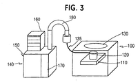
- Fig. 3 illustrates an exemplary application of the invention in conjunction with a test device comprising a wafer prober 100.
- the wafer prober 100 may be one of several that are available, such as a UF200 prober obtainable from Tokyo Seimitsu Co., Ltd. (TSK).
- the wafer prober 100 includes a stage 110 carrying a chuck 120.
- the chuck 120 is arranged to carry a wafer (not shown) on which a number of semiconductor integrated circuit devices have been formed.
- Such wafers are typically 200 mm in diameter although other sizes are often used, and can have more than 200 devices formed on them. The number and arrangement of devices on the wafer will vary according to the particular design of the IC device in question.
- the test device of Fig. 3 also comprises a test head interface 130 providing electrical connections, which may be applied to power and input/output pads on the devices on the wafer.
- the connections can be needles or any other form of contact appropriate to the device in question.
- the test head interface 130 is provided with connections for the test head of any of several available test systems, such as the ITS 9000 IX (not shown) of Schlumberger Technologies, Inc. of San Jose, California.
- the test device of Fig. 3 further comprises a temperature control system 140.
- the chuck 120 is connected by way of fluid supply lines and control cables contained in a housing 135 to the temperature control system 140.
- the temperature control system 140 may be implemented by any of several available systems, such as an ETC 1000 manufactured by Schlumberger Technologies, Inc.
- the temperature control system 140 comprises a thermal control chassis 150 carrying a system controller 160 provided with an operator interface, a liquid cooling and recirculation system 170, and a boom arm 180 supporting the fluid supply lines and control cables.
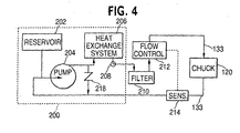
- Fig. 4 shows a block diagram of the liquid cooling and recirculating system 170.
- the liquid cooling and recirculating system 170 includes a chiller system 200, a filter 210, and a flow control 212.
- the chiller system comprises a pressurized coolant reservoir 202, a pump 204, a heat exchange (heating/cooling) system 206, a temperature sensor 208, and a pressure relief valve 218. Fluid passes from the chiller system 200, via the temperature sensor 208, through the filter 210 to the flow control 212 and on to the chuck 120. Fluid then returns from the chuck 120 and through a flow sensor 214 to be pumped around the liquid cooling and recirculating system 170 again.
- the flow sensor 214 can be placed in the path of the fluid flowing into the chuck 120, such as between the flow control 212 and the chuck 120.
- the flow sensor may also be implemented as part of the liquid cooling and recirculating system 170 in an alternative embodiment.
- the pressure relief valve 218 is disposed between the pump output and pump input to avoid accidentally overpressurizing the system.
- the fluid flows into and out of the heat exchanger 216 through the fluid supply lines 133.
- the heat exchanger 216 exchanges heat between the liquid cooling and recirculating system 170 and a DUT. In other embodiments, however, the heat exchanger 216 may include the liquid or the liquid cooling and recirculating system 170.
- the cooling fluid may be, for example, HFE7100 operating between - 40°C and +40°C, water/glycol or water/methanol mixtures operating between + 10°C and + 90°C, or any other suitable fluid depending on the desired temperature and heat dissipation required.
- HFE7100 is a specialty liquid manufactured by 3M corporation, which contains ethyl nonafluorobutylether and ethyl nonafluoroisobutylether.
- the difference between the device set point temperature and the fluid temperature can be in the range of 5°C to 160°C, with device set point temperatures typically in the range of -35°C to + 170°C.
- liquid circulating through the chuck 120 is cooled below a set point temperature.
- the heating element 149 of Fig. 2B which is in thermal contact with the chuck 120 and a DUT 182, is used to maintain the temperature of the DUT 182 at the set point temperature.
- the chuck 120 acts as a heat sink by absorbing heat energy from the heating element 149 and, at times, indirectly, from the test device 182.
- Fig. 6 shows a high level block diagram of the control electronics of the system controller 160 of the temperature control system 140 shown in Fig. 3.
- Variables in the control electronics system include (i) a signal V fsst , representing a system forcing temperature T fss of the heating element 149, measured by a temperature sensor in a heating element (not shown), (ii) a signal V Ped representing a device power consumption, P ed , measured by a monitoring circuit 250, which calculates the heat generated by the device (not shown) from the power drawn by the device during the test, and (iii) a signal V sp representing a device set-point temperature T sp , which is set by the user.
- V fsst representing a system forcing temperature T fss of the heating element 149
- P ed a device power consumption
- the thermal control circuit 252 generates a temperature control signal V tcs in a manner described below with respect to Fig. 9 and provides this signal to a heat exchanger temperature control 256 on the board 254.
- the heat exchanger temperature control 256 outputs a heater power signal V hps to a power amplifier 258, which provides a heater power I h to the heating element 149.
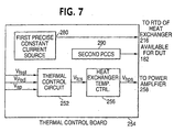
- Fig. 7 shows a more detailed block diagram of the thermal control board 254.
- the thermal control board 254 comprises, in addition to the thermal control circuit 252 and the heat exchanger temperature control 256, a first precise constant current source 280 and a second precise constant current source 290.
- the first precise constant current source 280 sends a precise constant current from the thermal control board 254 to a variable resistance device ("RTD") in the heating element 149.
- the RTD responds to the system forcing temperature and outputs a voltage representing the system forcing temperature V fsst .
- the system forcing temperature signal feeds back into the thermal control circuit 252. Separating the first precise constant current source 280 from the heater 149 allows in that the heater 149 to be replaced more easily.
- the second precise constant current source 290 is available to send a precise constant current to the DUT.
- thermal control board 254 Although only one thermal control board 254 is shown in Fig. 6, multiple boards can be provided. The use of multiple boards would allow simultaneous operation of a plurality of heating elements 149, each of which could be contained in the heat exchanger 216 and be thermally coupled to individual DUTs 182, as shown in Fig. 8A. Each separate board 254 would preferably have a separate set of inputs (V fsst , V Ped , V sp ) and the various values of V fsst would come from the plurality heating elements 149.
- Separate monitoring circuits 250 could be used to monitor the power of the individual DUTs 182, and separate power amplifiers 258 could be used for each heating element 149. It may be possible, however, for the separate power amplifiers 258 to be housed in a single device.
- Fig. 9 shows a more detailed block diagram of the thermal control circuit 252.
- Such thermal control circuit is described in more detail in commonly assigned U.S. Patent Application Serial No. 09/352,760 to Jones, et al ., titled "TEMPERATURE CONTROL OF ELECTRONIC DEVICES USING POWER FOLLOWING FEEDBACK," the disclosure of which is hereby fully incorporated as if fully set forth herein. That application discloses, among other things, a power following feedback control method.
- K theta is also derived from the general efficiency of the thermal control system when in contact with a DUT 182.
- the DUT 182 loses proportionally more heat to its surroundings, and the thermal control system must work harder to raise the DUT temperature than to lower it.
- the overall effect is the same as a lower thermal resistance between the DUT 182 and the heat exchanger 216 operating at an ambient set point.
- the DUT 182 gains heat from its surroundings, and the temperature control system 140 must work harder to lower temperature than to raise it.
- K theta is adjusted to reflect the effect of heat transfer to the DUT's surrounding environment during power excursions.
- K theta may be considered an effective or a fine-tuned thermal resistance of the medium.
- thermal resistance of different media are set out in standard chemistry reference books (such as CRC Handbook of Chemistry and Physics , 77 th Edition; David R. Lide, Editor-in-Chief)
- factors such as ambient humidity, pressure, and temperature may affect the actual thermal resistance.
- Thermal resistance may also be affected by the physical configuration of the test.
- To determine K theta one can use a calibration process to adjust the value of the anticipated thermal resistance of the medium and ascertain whether the result is an improvement.
- Another advantage of a calibration process is that it will automatically account for the "efficiency factor" of the heat transfer from the DUT 182 to the temperature control system 140 as a function of the set point temperature.
- K theta may incorporate the effects of a variety of variables into one term.
- K theta may be optimized for a given application, or type of DUT 182, and then can be used to test many different devices of the same type. Additionally, one practical effect of K theta is that in mirroring the monitored power consumption of the device with the temperature of the test device, K theta magnifies or compresses the relative magnitude of the mirroring.
- the power usage signal V Ped from the monitoring circuit 250 shown in Fig. 6 enters the thermal control circuit 252 by passing through a first amplifier 310. From there, the power usage signal passes into a multiplying circuit 320 where it is multiplied with V k-theta to create a first modified signal. The modified power usage signal then passes into a second amplifier 325 and from there into a thermal summing circuit 330. The voltage V fsst representing the system forcing temperature enters the thermal control circuit 252 by passing through a third amplifier 335. From there, V fsst passes into a subtracting circuit 340 where V IRO is subtracted from V fsst for a calibrated V fsst .
- the calibrated V fsst passes through a fourth amplifier 350 and into a divisional circuit 355 where the calibrated V fsst is divided by V alpha .
- a result representing (V fsst - V IRO )/V alpha passes through a fifth amplifier 365 and from there passes into the thermal summing circuit 330, and is summed there with the modified power usage signal to yield a summation.
- the summation passes into a differential circuit (or subtraction circuit) 375 which subtracts the summation from the set point temperature voltage, V sp , to yield a resulting signal.
- the resulting signal passes into a derivative circuit 380 which takes the derivative of the resulting signal with respect to time. This yields the temperature control signal V tcs which is amplified by a sixth amplifier 390 before being output from the thermal control circuit 252.
- test device which, among other things, allows the benefit of a heat exchanger to be applied to a wafer prober for temperature control of devices during testing.
- the present system is capable of providing a variety of other functions. Some of these additional functions include test control, temperature determination, and data acquisition.
- the preferred implementation comprises a liquid cooled heat exchanger and an electric heating element
- the exact method of providing cooling or heating can be chosen from any suitable source.
- heated liquids or gases can be used as the heating element.
- a feedback loop is used to control the operation of the heating element while the liquid cooled heat exchanger is operated as a set point heat sink.
- Other methods of control such as device power consumption monitoring or test power consumption profiling, can also be used.
- the present invention also provides a method for testing IC devices at wafer level in which the temperature of each device on the wafer is controlled independently of the other devices on the wafer during a test.
- the test can be run at high speed without the danger of heat damage to the devices.
- While the invention outlined above is discussed mainly in terms of wafer-level testing, it can also be applied to multiple singulated (that is, separated) devices. Preferably, these devices are arranged in a carrier in the same arrangement in which they were formed on the wafer. By retaining, during testing, the layout which the devices had on the wafer, production problems may be identified which depend on the position of a device on a wafer. This retention of the layout allows diagnosis of the production process and may improve yield.
Landscapes
- Engineering & Computer Science (AREA)
- Physics & Mathematics (AREA)
- Environmental & Geological Engineering (AREA)
- General Physics & Mathematics (AREA)
- Computer Hardware Design (AREA)
- Microelectronics & Electronic Packaging (AREA)
- General Engineering & Computer Science (AREA)
- Toxicology (AREA)
- Health & Medical Sciences (AREA)
- Testing Of Individual Semiconductor Devices (AREA)
- Testing Or Measuring Of Semiconductors Or The Like (AREA)
- Control Of Temperature (AREA)
- Semiconductor Integrated Circuits (AREA)
Claims (40)
- Vorrichtung für die Temperatursteuerung von integrierten Schaltkreiseinrichtungen (20) in der Prüfung, die aufweist:wobei die Temperatur von jedem der Mehrzahl von integrierten Schaltkreiseinrichtungen individuell an jeder der Mehrzahl von Regionen während der Prüfung gesteuert wird.einen Wärmetauscher (216) mit einer Oberfläche, die derart eingerichtet ist, daß sie mit jeder der Mehrzahl von integrierten Schaltkreiseinrichtungen in Kontakt tritt, wobei die Oberfläche eine Mehrzahl von Regionen hat, die jeweils einer der Mehrzahl von integrierten Schaltkreiseinrichtungen entsprechen, wobei der Wärmetauscher angepaßt ist, damit er eine gesteuerte Aufheizung und Abkühlung an diesen Regionen bereitstellt,
- Vorrichtung nach Anspruch 1, wobei der Wärmetauscher ein Chuck bzw. Futter (120) aufweist mit einer Mehrzahl von Heizelementen (149), die an jeder der Regionen angeordnet sind.
- Vorrichtung nach Anspruch 2, wobei das Futter eine Wärmesenke (10) beinhaltet, wobei jedes der Heizelemente die Temperatur eines der Bereiche bzw. einer der Regionen auf eine Temperatur oberhalb einer Temperatur, die von der Wärmesenke bestimmt wird, reguliert.
- Vorrichtung nach Anspruch 3, wobei die Wärmesenke eine Kavität (124) definiert, die derart angepaßt ist, daß sie mit einem temperaturgesteuerten Fluidstrom ausgestattet ist.
- Vorrichtung nach Anspruch 4, wobei die Temperatur des Fluids und der Heizelemente basierend auf dem Leistungsverbrauch der Mehrzahl von integrierten Schaltkreiseinrichtungen reguliert wird.
- Vorrichtung nach Anspruch 1, wobei eines der Mehrzahl von Heizelementen (149) an jeder der Mehrzahl von Regionen bereitgestellt wird.
- Vorrichtung nach Anspruch 1, wobei die Temperatur jeder Region individuell von einem Heizelement (149), das an einer Wärmesenke (10) angeordnet ist, gesteuert wird.
- Vorrichtung nach Anspruch 7, wobei jedes der Heizelemente über einer entsprechenden Wärmesenke von einer Mehrzahl von Wärmesenken angeordnet ist.
- Vorrichtung nach Anspruch 7, wobei jedes Heizelement über einer einzelnen Wärmesenke angeordnet ist.
- Vorrichtung nach einem der vorherigen Ansprüche, wobei die Temperatur von jeder der Mehrzahl von integrierten Schaltkreiseinrichtungen individuell gesteuert wird basierend auf dem Energieverbrauch der integrierten Schaltkreiseinrichtungen.
- Vorrichtung nach einem der Ansprüche 1 bis 10, wobei die Mehrzahl von integrierten Schaltkreiseinrichtungen auf einem Wafer ausgebildet ist und die Oberfläche so eingerichtet ist, daß sie den Wafer berührt, so daß die Mehrzahl von Regionen den jeweiligen Einrichtungen der Mehrzahl von integrierten Schaltkreiseinrichtungen, die auf dem Wafer gebildet sind, entspricht.
- Vorrichtung nach einem der Ansprüche 1 bis 10, wobei die Mehrzahl von integrierten Schaltkreiseinrichtungen singularisierte Einrichtungen sind und die Oberfläche derart eingerichtet ist, daß sie die singularisierten Einrichtungen kontaktiert, so daß die Mehrzahl von Regionen zu entsprechenden Einrichtungen der singularisierten Einrichtungen korrespondieren.
- Vorrichtung nach Anspruch 1, wobei der Wärmetauscher aufweist:ein Futter (120) für das Lokalisieren der Einrichtungen während der Prüfung undmehrere Temperatursteuervorrichtungen (149), um individuell die Temperatur von jeder der Mehrzahl von integrierten Schaltkreiseinrichtungen zu steuern, die in dem Futter angeordnet sind, um mit der Anordnung auf einem Wafer der zu testenden Einrichtungen zu korrespondieren.
- Vorrichtung nach Anspruch 13, wobei das Futter mit Einrichtungen für die Steuerung seiner Temperatur während des Prüfens ausgestattet ist.
- Vorrichtung nach Anspruch 14, wobei die Einrichtung für das Steuern der Futtertemperatur die Zuführung eines temperaturgesteuerten Fluids (170) beinhaltet.
- Vorrichtung nach Anspruch 14, wobei die Einrichtung für das Steuern der Futtertemperatur eine elektrische Heizeinrichtung (123) aufweist.
- Vorrichtung nach einem der Ansprüche 13 bis 16, wobei die mehreren Temperatursteuereinrichtungen Heizelemente (149) aufweisen.
- Vorrichtung nach Anspruch 17, die weiterhin zumindest eine Wärmesenke (10), die mit den Heizelementen verknüpft ist, aufweist.
- Vorrichtung nach Anspruch 18, wobei die zumindest eine Wärmesenke einen Körper aufweist, der mit einem Fluß von temperaturgesteuertem Fluid (170) ausgestattet ist.
- Vorrichtung nach Anspruch 18, wobei eine Wärmesenke für jedes Heizelement bereitgestellt wird.
- Vorrichtung nach Anspruch 18, wobei eine einzelne Wärmesenke für die mehreren Heizelemente bereitgestellt wird.
- Vorrichtung nach Anspruch 21, wobei die einzelne Wärmesenke in dem Futter aufgenommen ist.
- Vorrichtung nach Anspruch 22, wobei die Temperatur des Futters von einem temperaturgesteuerten Fluid (170) reguliert wird.
- Verfahren zum Steuern der Temperatur einer Mehrzahl von integrierten Schaltkreiseinrichtungen (20) während der Überprüfung, das aufweist:Plazieren der Mehrzahl von integrierten Schaltkreiseinrichtungen in Kontakt mit einer einer Mehrzahl von Regionen einer Oberfläche eines Wärmetauschers (216), die eingerichtet sind, um bei den Regionen ein gesteuertes Heizen und Kühlen bereitzustellen, undindividuelles Steuern der Temperatur von jeder der Mehrzahl von integrierten Schaltkreiseinrichtungen an jeder der Mehrzahl von Regionen.
- Verfahren nach Anspruch 24, wobei der Wärmetauscher ein Futter (120) mit einer Mehrzahl von Heizelementen (149), die an jeder der Regionen angeordnet sind, aufweist.
- Verfahren nach Anspruch 25, wobei das Futter eine Wärmesenke (10) aufweist und
wobei das Steuern das Regulieren der Temperatur einer entsprechenden der Regionen mit den Heizelementen bei einer Temperatur oberhalb einer Temperatur, die durch die Wärmesenke bestimmt wird, beinhaltet. - Verfahren nach Anspruch 26, wobei die Wärmesenke eine Kavität festlegt, die derart angepaßt ist, daß sie mit einem Fluß eines temperaturgesteuerten Fluids (170) ausgestattet ist.
- Verfahren nach Anspruch 24, das weiterhin aufweist:Bereitstellen von einem einer Mehrzahl von Heizelementen (149) an jeder der Mehrzahl von Regionen.
- Verfahren nach Anspruch 24, wobei die Temperatur von jeder Region einzeln von einem Heizelement (149), das auf einer Wärmesenke (10) angeordnet ist, gesteuert wird.
- Verfahren nach Anspruch 29, das weiterhin aufweist:Anordnen der Heizelemente mit einer entsprechenden der Mehrzahl von Wärmesenken.
- Verfahren nach Anspruch 29, das weiterhin aufweist:Anordnen der Heizelemente über einer einzelnen Wärmesenke.
- Verfahren nach einem der Ansprüche 24 bis 31, wobei die Mehrzahl von integrierten Schaltkreiseinrichtungen auf einem Wafer gebildet werden und die Oberfläche derart eingerichtet wird, daß sie den Wafer kontaktiert, so daß die Mehrzahl von Regionen entsprechenden Einrichtungen der Mehrzahl von integrierten Schaltkreiseinrichtungen, die auf dem Wafer ausgebildet sind, entspricht.
- Verfahren nach einem der Ansprüche 24 bis 31, wobei die Mehrzahl von integrierten Schaltkreiseinrichtungen singularisierte Einrichtungen sind und die Oberfläche derart angeordnet ist, daß sie die singularisierten Einrichtungen kontaktiert, so daß die Mehrzahl von Regionen entsprechenden Einrichtungen der singularisierten Einrichtungen entsprechen.
- Verfahren nach einem der Ansprüche 24 bis 33, wobei die Temperatur von jeder der Mehrzahl von integrierten Schaltkreiseinrichtungen individuell basierend auf dem Leistungsverbrauch der integrierten Schaltkreiseinrichtungen gesteuert wird.
- Verfahren nach Anspruch 24, wobei das Plazieren der Mehrzahl von integrierten Schaltkreiseinrichtungen aufweist:und wobei das Verfahren weiterhin aufweist:Lokalisieren der integrierten Schaltkreiseinrichtungen an einem Testort, an dem mehrere Temperatursteuereinrichtungen (149) angeordnet sind, so daß sie mit der Anordnung der integrierten Schaltkreiseinrichtungen, die getestet werden, korrespondieren,Testen einzelner der integrierten Schaltkreiseinrichtungen.
- Verfahren nach Anspruch 25, wobei die integrierten Schaltkreiseinrichtungen auf einem Wafer lokalisiert sind.
- Verfahren nach Anspruch 35, wobei die integrierten Schaltkreiseinrichtungen vor der Überprüfung singularisiert werden.
- Verfahren nach Anspruch 37, wobei die singularisierten Einrichtungen auf einem Futter in derselben Anordnung angeordnet sind, als ob sie auf einem Wafer ausgebildet wären.
- Verfahren nach einem der Ansprüche 35 bis 38, wobei das Lokalisieren der integrierten Schaltkreiseinrichtungen das Plazieren der Einrichtungen auf einem Futter (120) beinhaltet.
- Verfahren nach Anspruch 39, wobei das Futter mehrere Oberflächen hat, die zu jeder zu überprüfenden Einrichtung korrespondieren, wobei die Temperatur hiervon gesteuert wird, um die Temperatur der einzelnen Einrichtungen, die überprüft werden, zu steuern.
Applications Claiming Priority (3)
| Application Number | Priority Date | Filing Date | Title |
|---|---|---|---|
| US14393299P | 1999-07-15 | 1999-07-15 | |
| US143932P | 1999-07-15 | ||
| PCT/US2000/019161 WO2001006273A1 (en) | 1999-07-15 | 2000-07-14 | Apparatus and method for temperature control of ic device during test |
Publications (2)
| Publication Number | Publication Date |
|---|---|
| EP1196790A1 EP1196790A1 (de) | 2002-04-17 |
| EP1196790B1 true EP1196790B1 (de) | 2004-05-19 |
Family
ID=22506325
Family Applications (1)
| Application Number | Title | Priority Date | Filing Date |
|---|---|---|---|
| EP00947340A Expired - Lifetime EP1196790B1 (de) | 1999-07-15 | 2000-07-14 | Gerät und verfahren zur temperaturkontrolle von integrierten schaltungen während der prüfung |
Country Status (5)
| Country | Link |
|---|---|
| EP (1) | EP1196790B1 (de) |
| AT (1) | ATE267403T1 (de) |
| AU (1) | AU6096900A (de) |
| DE (1) | DE60010890T2 (de) |
| WO (1) | WO2001006273A1 (de) |
Cited By (1)
| Publication number | Priority date | Publication date | Assignee | Title |
|---|---|---|---|---|
| WO2023048644A3 (en) * | 2021-09-21 | 2023-05-11 | Aem Singapore Pte. Ltd. | Device and thermal tester for thermal testing dies of an integrated circuit |
Families Citing this family (9)
| Publication number | Priority date | Publication date | Assignee | Title |
|---|---|---|---|---|
| US6448992B1 (en) * | 2001-11-07 | 2002-09-10 | Advanced Micro Devices, Inc. | Voltage programmable power dissipater |
| JP4659328B2 (ja) * | 2002-10-21 | 2011-03-30 | 東京エレクトロン株式会社 | 被検査体を温度制御するプローブ装置 |
| DE102005001163B3 (de) | 2005-01-10 | 2006-05-18 | Erich Reitinger | Verfahren und Vorrichtung zum Testen von Halbleiterwafern mittels einer temperierbaren Aufspanneinrichtung |
| DE102005013926B4 (de) * | 2005-03-26 | 2011-06-22 | Jürgen Dipl.-Ing. 98693 Kröhnert | Vorrichtung und Verfahren zur Temperaturregelung eines Temperiergutes |
| US9335080B2 (en) * | 2011-10-17 | 2016-05-10 | Temptronic Corporation | Temperature system having an impurity filter |
| US20170261547A1 (en) * | 2016-03-08 | 2017-09-14 | Temptronic Corporation | Temperature Forcing System and Method with Conductive Thermal Probes |
| JP7266481B2 (ja) | 2019-07-19 | 2023-04-28 | 東京エレクトロン株式会社 | 温度制御装置、温度制御方法、および検査装置 |
| DE102021101240A1 (de) | 2021-01-21 | 2022-07-21 | TDK Europe GmbH | Testvorrichtung und Verfahren zum Betrieb der Testvorrichtung |
| CN114814543A (zh) * | 2022-04-22 | 2022-07-29 | 上海晶岳电子有限公司 | 一种电源管理芯片抗温度冲击测试系统及其测试方法 |
Family Cites Families (6)
| Publication number | Priority date | Publication date | Assignee | Title |
|---|---|---|---|---|
| US5084671A (en) * | 1987-09-02 | 1992-01-28 | Tokyo Electron Limited | Electric probing-test machine having a cooling system |
| US4870355A (en) * | 1988-01-11 | 1989-09-26 | Thermonics Incorporated | Thermal fixture for testing integrated circuits |
| US5210485A (en) * | 1991-07-26 | 1993-05-11 | International Business Machines Corporation | Probe for wafer burn-in test system |
| US5420520A (en) * | 1993-06-11 | 1995-05-30 | International Business Machines Corporation | Method and apparatus for testing of integrated circuit chips |
| DE19700839C2 (de) * | 1997-01-13 | 2000-06-08 | Siemens Ag | Chuckanordnung |
| US5911897A (en) * | 1997-01-13 | 1999-06-15 | Micro Control Company | Temperature control for high power burn-in for integrated circuits |
-
2000
- 2000-07-14 EP EP00947340A patent/EP1196790B1/de not_active Expired - Lifetime
- 2000-07-14 WO PCT/US2000/019161 patent/WO2001006273A1/en not_active Ceased
- 2000-07-14 AU AU60969/00A patent/AU6096900A/en not_active Abandoned
- 2000-07-14 AT AT00947340T patent/ATE267403T1/de not_active IP Right Cessation
- 2000-07-14 DE DE60010890T patent/DE60010890T2/de not_active Expired - Lifetime
Cited By (1)
| Publication number | Priority date | Publication date | Assignee | Title |
|---|---|---|---|---|
| WO2023048644A3 (en) * | 2021-09-21 | 2023-05-11 | Aem Singapore Pte. Ltd. | Device and thermal tester for thermal testing dies of an integrated circuit |
Also Published As
| Publication number | Publication date |
|---|---|
| DE60010890T2 (de) | 2005-05-19 |
| AU6096900A (en) | 2001-02-05 |
| ATE267403T1 (de) | 2004-06-15 |
| DE60010890D1 (de) | 2004-06-24 |
| EP1196790A1 (de) | 2002-04-17 |
| WO2001006273A1 (en) | 2001-01-25 |
| WO2001006273A9 (en) | 2002-07-11 |
Similar Documents
| Publication | Publication Date | Title |
|---|---|---|
| US6549026B1 (en) | Apparatus and method for temperature control of IC device during test | |
| CN100533165C (zh) | 执行电子器件的晶片级老化的方法 | |
| US6504392B2 (en) | Actively controlled heat sink for convective burn-in oven | |
| US7355428B2 (en) | Active thermal control system with miniature liquid-cooled temperature control device for electronic device testing | |
| KR101185536B1 (ko) | 온도가 조절될 수 있는 척 장치를 이용한 반도체 웨이퍼테스트 장치 및 방법 | |
| KR20220097269A (ko) | 장치 테스트를 위한 다중 입력 다중 구역 열 제어 | |
| US5001423A (en) | Dry interface thermal chuck temperature control system for semiconductor wafer testing | |
| TW496961B (en) | Device testing apparatus | |
| US6867611B2 (en) | Temperature-controlled thermal platform for automated testing | |
| JP6967067B2 (ja) | 個別に制御可能なヒータ素子のアレイを有する基板キャリア | |
| EP1196790B1 (de) | Gerät und verfahren zur temperaturkontrolle von integrierten schaltungen während der prüfung | |
| WO2001001460A9 (en) | Temperature controlled wafer chuck | |
| WO1999018447A1 (en) | Burn-in board with adaptable heat sink device | |
| KR20150095727A (ko) | 시험중인 장치를 위한 써멀 헤드 및 시험중인 장치의 온도를 제어하기 위한 방법 | |
| JP3611174B2 (ja) | 半導体ウェーハの温度試験装置 | |
| KR20250130649A (ko) | 검사 시스템 및 온도 제어 방법 | |
| JP3515904B2 (ja) | 半導体ウェーハの温度試験装置 | |
| O'Mathuna et al. | Test chips, test systems, and thermal test data for multichip modules in the ESPRIT-APACHIP project | |
| CN114630454A (zh) | 加热装置和led的控制方法 | |
| TW202516190A (zh) | 半導體晶圓測試裝置與半導體晶圓測試方法 | |
| JP2025144408A (ja) | 検査システム及び検査システムの温度制御方法 | |
| JP2026030402A (ja) | プローバ、及びその制御方法 | |
| TW202527146A (zh) | 多工熱控制晶圓及冷卻板 | |
| WO2025040957A1 (en) | Thermal control wafer with integrated heating-sensing elements | |
| O'Mathuna et al. | Test chips, test systems and thermal test data for multichip modules in the ESPRIT-APACHIP project |
Legal Events
| Date | Code | Title | Description |
|---|---|---|---|
| PUAI | Public reference made under article 153(3) epc to a published international application that has entered the european phase |
Free format text: ORIGINAL CODE: 0009012 |
|
| 17P | Request for examination filed |
Effective date: 20020201 |
|
| AK | Designated contracting states |
Kind code of ref document: A1 Designated state(s): AT BE CH CY DE DK ES FI FR GB GR IE IT LI LU MC NL PT SE |
|
| AX | Request for extension of the european patent |
Free format text: AL;LT;LV;MK;RO;SI |
|
| RAP1 | Party data changed (applicant data changed or rights of an application transferred) |
Owner name: DELTA DESIGN, INC. |
|
| 17Q | First examination report despatched |
Effective date: 20021118 |
|
| GRAP | Despatch of communication of intention to grant a patent |
Free format text: ORIGINAL CODE: EPIDOSNIGR1 |
|
| GRAS | Grant fee paid |
Free format text: ORIGINAL CODE: EPIDOSNIGR3 |
|
| GRAA | (expected) grant |
Free format text: ORIGINAL CODE: 0009210 |
|
| AK | Designated contracting states |
Kind code of ref document: B1 Designated state(s): AT BE CH CY DE DK ES FI FR GB GR IE IT LI LU MC NL PT SE |
|
| PG25 | Lapsed in a contracting state [announced via postgrant information from national office to epo] |
Ref country code: CY Free format text: LAPSE BECAUSE OF FAILURE TO SUBMIT A TRANSLATION OF THE DESCRIPTION OR TO PAY THE FEE WITHIN THE PRESCRIBED TIME-LIMIT Effective date: 20040519 Ref country code: BE Free format text: LAPSE BECAUSE OF FAILURE TO SUBMIT A TRANSLATION OF THE DESCRIPTION OR TO PAY THE FEE WITHIN THE PRESCRIBED TIME-LIMIT Effective date: 20040519 Ref country code: AT Free format text: LAPSE BECAUSE OF FAILURE TO SUBMIT A TRANSLATION OF THE DESCRIPTION OR TO PAY THE FEE WITHIN THE PRESCRIBED TIME-LIMIT Effective date: 20040519 Ref country code: CH Free format text: LAPSE BECAUSE OF FAILURE TO SUBMIT A TRANSLATION OF THE DESCRIPTION OR TO PAY THE FEE WITHIN THE PRESCRIBED TIME-LIMIT Effective date: 20040519 Ref country code: LI Free format text: LAPSE BECAUSE OF FAILURE TO SUBMIT A TRANSLATION OF THE DESCRIPTION OR TO PAY THE FEE WITHIN THE PRESCRIBED TIME-LIMIT Effective date: 20040519 Ref country code: NL Free format text: LAPSE BECAUSE OF FAILURE TO SUBMIT A TRANSLATION OF THE DESCRIPTION OR TO PAY THE FEE WITHIN THE PRESCRIBED TIME-LIMIT Effective date: 20040519 Ref country code: FI Free format text: LAPSE BECAUSE OF FAILURE TO SUBMIT A TRANSLATION OF THE DESCRIPTION OR TO PAY THE FEE WITHIN THE PRESCRIBED TIME-LIMIT Effective date: 20040519 Ref country code: IT Free format text: LAPSE BECAUSE OF FAILURE TO SUBMIT A TRANSLATION OF THE DESCRIPTION OR TO PAY THE FEE WITHIN THE PRESCRIBED TIME-LIMIT;WARNING: LAPSES OF ITALIAN PATENTS WITH EFFECTIVE DATE BEFORE 2007 MAY HAVE OCCURRED AT ANY TIME BEFORE 2007. THE CORRECT EFFECTIVE DATE MAY BE DIFFERENT FROM THE ONE RECORDED. Effective date: 20040519 |
|
| REG | Reference to a national code |
Ref country code: GB Ref legal event code: FG4D |
|
| REG | Reference to a national code |
Ref country code: CH Ref legal event code: EP |
|
| REG | Reference to a national code |
Ref country code: IE Ref legal event code: FG4D |
|
| REF | Corresponds to: |
Ref document number: 60010890 Country of ref document: DE Date of ref document: 20040624 Kind code of ref document: P |
|
| PG25 | Lapsed in a contracting state [announced via postgrant information from national office to epo] |
Ref country code: LU Free format text: LAPSE BECAUSE OF NON-PAYMENT OF DUE FEES Effective date: 20040714 Ref country code: IE Free format text: LAPSE BECAUSE OF NON-PAYMENT OF DUE FEES Effective date: 20040714 |
|
| PG25 | Lapsed in a contracting state [announced via postgrant information from national office to epo] |
Ref country code: MC Free format text: LAPSE BECAUSE OF NON-PAYMENT OF DUE FEES Effective date: 20040731 |
|
| PG25 | Lapsed in a contracting state [announced via postgrant information from national office to epo] |
Ref country code: SE Free format text: LAPSE BECAUSE OF FAILURE TO SUBMIT A TRANSLATION OF THE DESCRIPTION OR TO PAY THE FEE WITHIN THE PRESCRIBED TIME-LIMIT Effective date: 20040819 Ref country code: DK Free format text: LAPSE BECAUSE OF FAILURE TO SUBMIT A TRANSLATION OF THE DESCRIPTION OR TO PAY THE FEE WITHIN THE PRESCRIBED TIME-LIMIT Effective date: 20040819 Ref country code: GR Free format text: LAPSE BECAUSE OF FAILURE TO SUBMIT A TRANSLATION OF THE DESCRIPTION OR TO PAY THE FEE WITHIN THE PRESCRIBED TIME-LIMIT Effective date: 20040819 |
|
| PG25 | Lapsed in a contracting state [announced via postgrant information from national office to epo] |
Ref country code: ES Free format text: LAPSE BECAUSE OF FAILURE TO SUBMIT A TRANSLATION OF THE DESCRIPTION OR TO PAY THE FEE WITHIN THE PRESCRIBED TIME-LIMIT Effective date: 20040830 |
|
| LTIE | Lt: invalidation of european patent or patent extension |
Effective date: 20040519 |
|
| NLV1 | Nl: lapsed or annulled due to failure to fulfill the requirements of art. 29p and 29m of the patents act | ||
| REG | Reference to a national code |
Ref country code: CH Ref legal event code: PL |
|
| ET | Fr: translation filed | ||
| PLBE | No opposition filed within time limit |
Free format text: ORIGINAL CODE: 0009261 |
|
| STAA | Information on the status of an ep patent application or granted ep patent |
Free format text: STATUS: NO OPPOSITION FILED WITHIN TIME LIMIT |
|
| REG | Reference to a national code |
Ref country code: IE Ref legal event code: MM4A |
|
| 26N | No opposition filed |
Effective date: 20050222 |
|
| PG25 | Lapsed in a contracting state [announced via postgrant information from national office to epo] |
Ref country code: PT Free format text: LAPSE BECAUSE OF NON-PAYMENT OF DUE FEES Effective date: 20041019 |
|
| PGFP | Annual fee paid to national office [announced via postgrant information from national office to epo] |
Ref country code: GB Payment date: 20070720 Year of fee payment: 8 |
|
| PGFP | Annual fee paid to national office [announced via postgrant information from national office to epo] |
Ref country code: FR Payment date: 20070710 Year of fee payment: 8 |
|
| GBPC | Gb: european patent ceased through non-payment of renewal fee |
Effective date: 20080714 |
|
| REG | Reference to a national code |
Ref country code: FR Ref legal event code: ST Effective date: 20090331 |
|
| PG25 | Lapsed in a contracting state [announced via postgrant information from national office to epo] |
Ref country code: GB Free format text: LAPSE BECAUSE OF NON-PAYMENT OF DUE FEES Effective date: 20080714 |
|
| PG25 | Lapsed in a contracting state [announced via postgrant information from national office to epo] |
Ref country code: FR Free format text: LAPSE BECAUSE OF NON-PAYMENT OF DUE FEES Effective date: 20080731 |
|
| PGFP | Annual fee paid to national office [announced via postgrant information from national office to epo] |
Ref country code: DE Payment date: 20100723 Year of fee payment: 11 |
|
| PG25 | Lapsed in a contracting state [announced via postgrant information from national office to epo] |
Ref country code: DE Free format text: LAPSE BECAUSE OF NON-PAYMENT OF DUE FEES Effective date: 20120201 |
|
| REG | Reference to a national code |
Ref country code: DE Ref legal event code: R119 Ref document number: 60010890 Country of ref document: DE Effective date: 20120201 |