EP1202345A2 - Leistungshalbleiterelement-Wärmeleitplatte, Leitplatte dafür, Kühlkörpermaterial und Lotmaterial - Google Patents
Leistungshalbleiterelement-Wärmeleitplatte, Leitplatte dafür, Kühlkörpermaterial und Lotmaterial Download PDFInfo
- Publication number
- EP1202345A2 EP1202345A2 EP01125817A EP01125817A EP1202345A2 EP 1202345 A2 EP1202345 A2 EP 1202345A2 EP 01125817 A EP01125817 A EP 01125817A EP 01125817 A EP01125817 A EP 01125817A EP 1202345 A2 EP1202345 A2 EP 1202345A2
- Authority
- EP
- European Patent Office
- Prior art keywords
- plate
- heat sink
- aluminum
- alloy
- solder
- Prior art date
- Legal status (The legal status is an assumption and is not a legal conclusion. Google has not performed a legal analysis and makes no representation as to the accuracy of the status listed.)
- Withdrawn
Links
Images


Classifications
-
- H—ELECTRICITY
- H10—SEMICONDUCTOR DEVICES; ELECTRIC SOLID-STATE DEVICES NOT OTHERWISE PROVIDED FOR
- H10W—GENERIC PACKAGES, INTERCONNECTIONS, CONNECTORS OR OTHER CONSTRUCTIONAL DETAILS OF DEVICES COVERED BY CLASS H10
- H10W72/00—Interconnections or connectors in packages
- H10W72/30—Die-attach connectors
-
- H—ELECTRICITY
- H10—SEMICONDUCTOR DEVICES; ELECTRIC SOLID-STATE DEVICES NOT OTHERWISE PROVIDED FOR
- H10W—GENERIC PACKAGES, INTERCONNECTIONS, CONNECTORS OR OTHER CONSTRUCTIONAL DETAILS OF DEVICES COVERED BY CLASS H10
- H10W40/00—Arrangements for thermal protection or thermal control
- H10W40/20—Arrangements for cooling
- H10W40/25—Arrangements for cooling characterised by their materials
- H10W40/255—Arrangements for cooling characterised by their materials having a laminate or multilayered structure, e.g. direct bond copper [DBC] ceramic substrates
-
- H—ELECTRICITY
- H05—ELECTRIC TECHNIQUES NOT OTHERWISE PROVIDED FOR
- H05K—PRINTED CIRCUITS; CASINGS OR CONSTRUCTIONAL DETAILS OF ELECTRIC APPARATUS; MANUFACTURE OF ASSEMBLAGES OF ELECTRICAL COMPONENTS
- H05K1/00—Printed circuits
- H05K1/02—Details
- H05K1/03—Use of materials for the substrate
- H05K1/0306—Inorganic insulating substrates, e.g. ceramic, glass
-
- H—ELECTRICITY
- H05—ELECTRIC TECHNIQUES NOT OTHERWISE PROVIDED FOR
- H05K—PRINTED CIRCUITS; CASINGS OR CONSTRUCTIONAL DETAILS OF ELECTRIC APPARATUS; MANUFACTURE OF ASSEMBLAGES OF ELECTRICAL COMPONENTS
- H05K3/00—Apparatus or processes for manufacturing printed circuits
- H05K3/0058—Laminating printed circuit boards onto other substrates, e.g. metallic substrates
-
- H—ELECTRICITY
- H05—ELECTRIC TECHNIQUES NOT OTHERWISE PROVIDED FOR
- H05K—PRINTED CIRCUITS; CASINGS OR CONSTRUCTIONAL DETAILS OF ELECTRIC APPARATUS; MANUFACTURE OF ASSEMBLAGES OF ELECTRICAL COMPONENTS
- H05K3/00—Apparatus or processes for manufacturing printed circuits
- H05K3/38—Improvement of the adhesion between the insulating substrate and the metal
-
- H—ELECTRICITY
- H10—SEMICONDUCTOR DEVICES; ELECTRIC SOLID-STATE DEVICES NOT OTHERWISE PROVIDED FOR
- H10W—GENERIC PACKAGES, INTERCONNECTIONS, CONNECTORS OR OTHER CONSTRUCTIONAL DETAILS OF DEVICES COVERED BY CLASS H10
- H10W70/00—Package substrates; Interposers; Redistribution layers [RDL]
- H10W70/60—Insulating or insulated package substrates; Interposers; Redistribution layers
- H10W70/67—Insulating or insulated package substrates; Interposers; Redistribution layers characterised by their insulating layers or insulating parts
- H10W70/68—Shapes or dispositions thereof
- H10W70/685—Shapes or dispositions thereof comprising multiple insulating layers
-
- H—ELECTRICITY
- H10—SEMICONDUCTOR DEVICES; ELECTRIC SOLID-STATE DEVICES NOT OTHERWISE PROVIDED FOR
- H10W—GENERIC PACKAGES, INTERCONNECTIONS, CONNECTORS OR OTHER CONSTRUCTIONAL DETAILS OF DEVICES COVERED BY CLASS H10
- H10W72/00—Interconnections or connectors in packages
- H10W72/071—Connecting or disconnecting
- H10W72/073—Connecting or disconnecting of die-attach connectors
-
- H—ELECTRICITY
- H10—SEMICONDUCTOR DEVICES; ELECTRIC SOLID-STATE DEVICES NOT OTHERWISE PROVIDED FOR
- H10W—GENERIC PACKAGES, INTERCONNECTIONS, CONNECTORS OR OTHER CONSTRUCTIONAL DETAILS OF DEVICES COVERED BY CLASS H10
- H10W72/00—Interconnections or connectors in packages
- H10W72/30—Die-attach connectors
- H10W72/321—Structures or relative sizes of die-attach connectors
- H10W72/325—Die-attach connectors having a filler embedded in a matrix
-
- H—ELECTRICITY
- H10—SEMICONDUCTOR DEVICES; ELECTRIC SOLID-STATE DEVICES NOT OTHERWISE PROVIDED FOR
- H10W—GENERIC PACKAGES, INTERCONNECTIONS, CONNECTORS OR OTHER CONSTRUCTIONAL DETAILS OF DEVICES COVERED BY CLASS H10
- H10W72/00—Interconnections or connectors in packages
- H10W72/30—Die-attach connectors
- H10W72/351—Materials of die-attach connectors
- H10W72/352—Materials of die-attach connectors comprising metals or metalloids, e.g. solders
-
- H—ELECTRICITY
- H10—SEMICONDUCTOR DEVICES; ELECTRIC SOLID-STATE DEVICES NOT OTHERWISE PROVIDED FOR
- H10W—GENERIC PACKAGES, INTERCONNECTIONS, CONNECTORS OR OTHER CONSTRUCTIONAL DETAILS OF DEVICES COVERED BY CLASS H10
- H10W72/00—Interconnections or connectors in packages
- H10W72/30—Die-attach connectors
- H10W72/381—Auxiliary members
Definitions
- the present invention relates to a novel power module mounting semiconductor power elements, and to a novel heat dissipation board used for the power module, and to a conductor plate and a heat sink and a solder material and a composite plate used for the heat dissipation board.
- Heat dissipation boards for semiconductor power element having a structure of laminating a conductor plate, a ceramic plate and a heat sink plate have been known.
- Various kinds of materials are used for the conductor plate, the ceramic plate and the heat sink plate, and various methods are used for bonding between the conductor plate and the ceramic plate and between the ceramic plate and the heat sink plate.
- heat dissipation boards using an aluminum alloy group solder for bonding are disclosed in Japanese Patent Application Laid-Open No.3-125463, Japanese Patent Application Laid-Open No.4-12554, Japanese Patent Application Laid-Open No.9-27572, Japanese Patent Application Laid-Open No.10-65075, Japanese Patent Application Laid-Open No.11-220073 and Japanese Patent Application Laid-Open No.2000-119071.
- the conventional heat dissipation boards for semiconductor power element have had the significant problems relating to the productivity and the reliability.
- An object of the present invention is to provide a semiconductor power element heat dissipation board which has a high bonding strength without voids in the bonding portion, and prevents forming of a brittle Al/Cu intermetallic chemical compound, and has high reliability, and of which the manufacturing method is simple, and to provide a conductor plate and a heat sink plate and a solder used for the semiconductor power element heat dissipation board, and to provide a power module and a composite plate using the semiconductor power element heat dissipation board.
- the semiconductor power element heat dissipation board in accordance with the present invention has no void in the bonding portion and has a high bonding strength of at least 10 MPa or larger through bonding capable of suppressing aluminum diffusion by employing any one of or combination of providing a diffusion suppression member for suppressing diffusion of aluminum; using a low melting point aluminum alloy group solder; using an aluminum alloy group solder provided onto a core member or the conductor plate made of aluminum or an aluminum alloy; and pressing by adding a load at bonding.
- the above-mentioned conductor plate is made of any one of copper, a copper alloy, a laminated member of copper and aluminum, aluminum, an aluminum alloy, and a laminated member of a copper alloy and an aluminum alloy. It is also preferable that the above-mentioned ceramic plate is made of any one of alumina, aluminum nitride and silicon nitride, and the above-mentioned conductor plate is made of any one of copper, a copper alloy, aluminum, an aluminum alloy, an Al-SiC composite material, and a composite material of copper and cuprous oxide.
- the above-mentioned aluminum alloy group solder portion between the ceramic plate and the heat sink plate is projected by at least 1 millimeter or more from the end portion of the ceramic plate or is depressed by at least 1 millimeter or more; and that the conductor plate, the ceramic plate and the heat sink plate are successively laminated, and then these plate are bonded using the aluminum alloy group solder under a vacuum atmosphere or an inert atmosphere; and that the conductor plate, the ceramic plate and the heat sink plate are bonded using the aluminum alloy group solder by heating the laminated body under a vacuum atmosphere or an inert atmosphere while a load is being added to the laminated body.
- the present invention is characterized by that the aluminum alloy group solder portion is formed by pre-cladding the aluminum alloy group solder on one surface or both surfaces of a core material portion made of aluminum or an aluminum alloy, and a surface of at least any one of the conductor plate and the heat sink plate opposite to the aluminum alloy group solder portion is coated with a diffusion suppression member for suppressing diffusion between the conductor plate or the heat sink plate and aluminum in the solder; or by that the conductor plate is integrated with the diffusion suppression member for suppressing diffusion between the conductor plate and aluminum in the solder to form a one-piece structure; or by that the solder material portion is formed of a clad member which is bonded to the conductor plate through the diffusion suppression member for suppressing diffusion between
- the present invention is characterized by that a diffusion suppression member for suppressing diffusion between the conductor plate made of copper or a copper alloy and aluminum in the solder is provided between the conductor plate made of copper or a copper alloy and the conductor plate made of aluminum or an aluminum alloy or between the conductor plate made of copper or a copper alloy and the core member, or by that nickel is plated on a surface of the conductor plate opposite to a surface of the conductor
- the present invention is characterized by that a diffusion suppression member for suppressing diffusion of aluminum in the solder to the heat sink plate is provided on a bonding side surface of the ceramic plate.
- the present invention is characterized by that the aluminum alloy group solder has a melting point lower than 500 °C, and working temperature at bonding is low temperature of 400 °C class; or by that the aluminum alloy group solder has a melting point lower than 500 °C, and working temperature at bonding is low temperature of 400 °C class, and the aluminum alloy group solder portion is pre-cladded on one surface or on the both surfaces of a core material portion made of aluminum or an aluminum alloy.
- the productivity of the semiconductor power element heat dissipation board and the conductor plate could be improved, and at the same time, a high bonding strength without voids can be obtained. Accordingly, the troubles such as separation of the bonding portion caused by thermal stress produced in the bonding portion can be eliminated even if the semiconductor power element heat dissipation board is used under a very severe environment having a very large number of thermal shocks.
- Embodiments 1 to 10 relating to aluminum alloy group solders of which the melting point is about 580 °C and the working temperature at bonding is 500 °C or higher.
- FIG. 1 is a cross-sectional view showing an embodiment of a semiconductor power element heat dissipation board in accordance with the present invention.
- the semiconductor power element heat dissipation board has the structure that a conductor plate 6, a ceramic plate 3 and a heat sink plate 1 are laminated, and then these plates are bonded together using aluminum alloy group solder portions 2 and 4.
- the conductor plate 6 has a nickel plated film 7 (the thickness is several to 10 ⁇ m) on a surface opposite to a surface in contact with the ceramic plate 3, and also has a diffusion suppression member 5 for preventing a component of the conductor plate 6 from diffusing to aluminum in the aluminum alloy group solder 4 or for suppressing the effect of diffusion to aluminum on the surface in contact with the ceramic plate 3.
- the diffusion suppression member 5 is made of at least one kind of material selected from the group consisting of pure Ni, pure Cr, pure Ti, pure W, an Ni alloy, a Cr alloy, a Ti alloy and a W alloy, and the thickness is at least 5 ⁇ m or thicker in the case of pure nickel, and around several ⁇ m in the cases of the other materials.
- Materials generally used for the heat sink plate 1 are copper, a copper alloy, aluminum and an aluminum alloy. In the case of using aluminum or an aluminum alloy, the aluminum in the heat sink plate only diffuses mutually with the aluminum in the aluminum alloy group solder 2. Therefore, the diffusion suppression member for preventing diffusing to aluminum or suppressing the effect of diffusion to aluminum is not necessary.
- the solder portions of the aluminum alloy group solder portions 2 and 4 are made of an Al-Si alloy, an Al-Si-Mg alloy, am Al-Ge alloy or an Al-Si-Ge alloy.
- the eutectic temperature (melting temperature) is about 580 °C.
- a load adding jig (not shown in the figure) made of ceramic such as alumina, not react with nickel, was brought in contact with the nickel plated film 7 formed on the surface of the conductor plate 6, and then these laminated plates were heated up to 580 °C to 610 °C under a vacuum atmosphere or an inert atmosphere and under a bonding condition of adding a load of 0.1 to 10 MPa per unit area.
- a high reliable semiconductor power element heat dissipation board could be obtained.
- FIG. 2 is an exploded cross-sectional view showing the semiconductor power element heat dissipation board of FIG. 1 before bonding.
- the conductor plate 6 having the nickel plated film 7 formed on one surface and a film of the diffusion suppression member formed on the other surface is indicated by a conductor plate portion assembly 100.
- the plates After laminating the aluminum alloy group solder 2, the ceramic plate 3, the aluminum alloy group solder 4, the conductor plate portion assembly 100 on the heat sink plate 1 in this order, the plates are bonded under the above-mentioned condition.
- the manufacturing method is good in the productivity because the aluminum alloy group solder portions 2 and 4 are films but not printed parts.
- FIG. 3 is detailed cross-sectional views showing the aluminum alloy group solder portions 2 and 4.
- FIG. 3 (a) is a cross-sectional view showing a composite solder portion which is formed by pre-cladding thin films of aluminum alloy group solder portions 9 and 10 on the both surfaces of a core portion 8 made of aluminum or an aluminum alloy through rolling.
- the clad member composed of laminated pieces of the solder portion 9/- the core material portion 8/ the solder portion 10 is a film having a total thickness of hundred to hundreds micrometers, and the thickness of the solder portions 9 and 10 is about 10 % as thin as the thickness of the core material portion 8.
- the solder portions 9, 10 are made of an Al-Si alloy, Al-Si-Mg alloy, an Al-Ge alloy or an Al-Si-Ge alloy.
- the eutectic temperature (melting temperature) of the solder portions is about 580 °C which is lower than the aluminum melting temperature of 660 °C of the core material portion.
- the core material portion may have the aluminum alloy group solder portion 9 or 10.
- the core material portion 8 made of an aluminum alloy is in the solid phase under the melting temperature of the aluminum alloy group solder portions 9 and 10, and is in the solid phase at the bonding temperature, and has the melting temperature higher than the bonding temperature. Further, when the same element is added to these aluminum alloys, the content in the aluminum alloy of the core material portion 8 is smaller than the content in the aluminum alloy of the aluminum alloy group solder portions 9, 10. When the other element is added, the content is adjusted depending the purpose.
- the laminated body is heated up to a high temperature of 580 °C to 610 °C under a vacuum atmosphere or an inert atmosphere after forming the laminated body by laminating the conductor plate 6, the ceramic plate 3 and the heat sink plate 1, only the solder portions are melted but the core material portion is not melted.
- the solder portions 9 and 10 could be prevented from flowing out from the bonding portions to the external because the thickness of the solder portions 9 and 10 was about 10 % as thin as the thickness of the core material portion 8 even under the bonding condition of adding a load of 0.1 to 10 MPa per unit area.
- the clad member composed of laminated pieces of the solder portion/ the core material portion/ the solder portion had a very small amount of voids produced in the bonding portion and had no troubles such as incapability of bonding, the clad member was very effective as an aluminum alloy group solder member for materializing a high reliable semiconductor power element heat dissipation board capable of obtaining a bonding strength higher than several tens MPa.
- FIG. 3 (b) shows an aluminum alloy group solder portion 2 or 4 without any core material portion.
- the solder portion 11 is totally made of a solder material which melts at a temperature under the bonding condition.
- the bonding strength could be secured without the core material portion when the thickness of the solder portion 11 was thinner than several tens micrometer though a small amount of voids were produced.
- the bonding load per unit area was required to be decreased as low as possible.
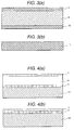
- FIG. 4 is a cross-sectional view showing other embodiments of conductor plate portion assemblies 100 of the conductor plate 6.
- the conductor plate portion assembly 100 of FIG. 4 (a) is constructed by forming a nickel plated film 7 on one surface of the conductor plate 6 made of copper or a copper alloy, and by forming a film of the diffusion suppression member 5 for preventing copper from diffusing to the aluminum conductor plate 12 or for suppressing the effect of the copper diffusion to the aluminum conductor plate 12 on the other surface through plating or sputtering.
- the conductor plate portion assembly 100 in this figure can be obtained by forming the film of the diffusion suppression member 5 on the conductor plate 6, and then by forming a nickel film 7 through plating on a clad member having the aluminum conductor plate 12 firmly bonded to the conductor plate through rolling. Otherwise, the conductor plate portion assembly 100 in this figure can be obtained by bonding the tree layer materials of a film to be formed in the conductor plate 6, the diffusion suppression member 5 and the aluminum conductor plate 12 through rolling at a time, and then by forming the nickel film 7 through plating. Therein, the thickness of the conductor plate 6 made of copper or a copper alloy and the thickness of the aluminum conductor plate 12 are nearly equal to each other and 150 to 250 ⁇ m, respectively.
- the conductor plate portion assembly 100 of FIG. 4 (b) is constructed by forming a film of the diffusion suppression member 5 on the surface of the aluminum conductor plate having a thickness of 300 to 500 ⁇ m, and then forming the nickel film 7 on the surface of the diffusion suppression member 5 through plating.
- the role of the diffusion suppression member 5 in this figure is to prevent diffusion of nickel in the nickel film 7 to the aluminum conductor 12 or to suppress the effect of the diffusion to the aluminum conductor 12. Therein, when the thickness of the nickel film 7 was thicker than 10 ⁇ m, it was experimentally found that the diffusion suppression member 5 might be eliminated.
- the aluminum conductor plate 12 on FIG. 4 (b) may be formed of an aluminum alloy as well as pure aluminum.
- the ill influence of the thermal stress due to the thermal expansion difference between the conductor plate portion assembly 100 and the ceramic plate 3 to the bonding portion between them could be reduced compared to the case where the conductor plate 6 of FIG. 1 was formed of the major material of copper or a copper alloy.
- the high reliability could be secured even if the semiconductor power element heat dissipation board was used under a severe environment having a large number of thermal shocks.
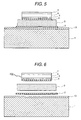
- FIG. 5 is a cross-sectional view showing another embodiment of a semiconductor power element heat dissipation board in accordance with the present invention.
- the semiconductor power element heat dissipation board in this figure is different from the heat dissipation board shown in FIG. 1 in the following two points.
- the first different points are that copper, a copper alloy or a copper composite material is used as the material for the heat sink plate 1, and a film of the diffusion suppression member 13 for preventing copper from diffusing to aluminum in the aluminum alloy group solder 2 or for suppressing the effect of diffusion to aluminum is formed on the surface of the ceramic plate 3.
- the diffusion suppression member 13 is made of at least one kind of material selected from the group consisting of pure Ni, pure Cr, pure Ti, pure W, an Ni alloy, a Cr alloy, a Ti alloy and a W alloy, and the thickness is at least 5 ⁇ m or thicker in the case of pure nickel, and around several micrometers in the cases of the other materials.
- the second different points are that before bonding the conductor plate 6 to the ceramic plate 3, a clad member formed in advance by inserting the diffusion suppression member 5 between the conductor plate 6 and the aluminum alloy group solder 4 and then bonding these plates through rolling. After that, a nickel plated film 7 is formed on one surface of the conductor plate 6, and then the clad member is formed in a desired dimension through punching work using a press and laminated on the ceramic plate 3 to be bonded.
- FIG. 6 is an exploded cross-sectional view showing the semiconductor power element heat dissipation board of FIG. 5 before bonding.
- the laminated body of the nickel film 7, the conductor plate 6, the diffusion suppression member 5 and the aluminum alloy group solder 4 is indicated by a conductor plate portion assembly 200.
- the conductor plate portion assembly 200 is formed in a desired dimension through punching work using the press after forming the nickel plated film 7 on one surface of the clad member.
- the problem of displacement at laminating can be completely eliminated, and number of the laminating processes can be decreased compared to the case of FIG. 1. Accordingly, it is possible to realize the manufacturing method capable of securing a high bonding strength, suitable for the mass production and having a high yield.
- the heat sink plate 1 is made of copper or a copper alloy, and integrated with the diffusion suppression member 5 attached in the bonding side by the aluminum alloy group solder 4 in a one-piece structure.
- the aluminum alloy group solder member 4 can employ those shown in FIG. 3 (a) and (b), similarly to Embodiment 1.
- FIG. 7 is a cross-sectional view showing other embodiments of the conductor plate portion assemblies 200.
- the conductor plate portion assembly 200 in FIG. 7 (a) is a clad member formed by inserting the diffusion suppression member 5 between the conductor plate 6 made of copper or a copper alloy and the aluminum alloy group solder member having a solder portion 10 formed on one surface of the core material portion 8 made of aluminum or an aluminum alloy, and firmly bonding the conductor plate 6, the diffusion suppression member 5 and the solder member, and then forming the nickel plated film 7 on the surface of the conductor plate 6.
- the conductor plate portion assembly shown in the figure can be obtained by forming the clad member into a desired dimension by punching work using a press.
- the diffusion suppression member 5 is formed of the same material as the above-mentioned material preventing diffusion of copper to aluminum of the core material portion 8 or suppressing the effect of diffusion to the aluminum, and the thickness is at least 5 ⁇ m or thicker in the case of pure nickel, and above several ⁇ m in the cases of the other materials.
- the thickness of the conductor plate 6 is several hundreds ⁇ m which is several times as thick as the thickness of the core material portion 8.
- the conductor plate portion assembly 200 in FIG. 7 (b) is different from that shown in FIG. 7 (a) in the following point. That is, the clad member is formed by replacing the core material portion 8 by the aluminum conductor plate 12 made of aluminum or an aluminum alloy, and the nickel plated film 7, the conductor plate 6 made of copper or a copper alloy, the diffusion suppression member 5, the aluminum conductor plate 12 made of aluminum or an aluminum alloy and the aluminum alloy group solder 10 are successively laminated.
- the thickness of the conductor plate 6 made of copper or a copper alloy and the thickness of the aluminum conductor plate 12 in the figure are nearly equal to each other and nearly 150 to 250 ⁇ m, respectively.
- the conductor plate portion assembly 200 in FIG. 7 (c) is different from that shown in FIG. 7 (b) in the following point. That is, the clad member is formed by removing the conductor plate 6 from the clad member of FIG. 7 (b), and the nickel plated film 7, the diffusion suppression member 5, the aluminum conductor plate 12 made of aluminum or an aluminum alloy and the aluminum alloy group solder 10 are successively laminated. The thickness of the aluminum conductor plate 12 in the figure is nearly equal to each other and nearly 300 to 500 ⁇ m.
- the main current flow paths of FIG. 7 (a), FIG. 7 (b) and FIG. 7 (c) are the conductor plate 6, the conductor plate 6/ the aluminum conductor plate 12, and the aluminum plate 12, respectively. In this embodiment, a high bonding strength can be also obtained.
- FIG. 8 is a cross-sectional view showing another embodiment of a semiconductor power element heat dissipation board in accordance with the present invention.
- the semiconductor power element heat dissipation board in this figure is different from the heat dissipation board shown in FIG. 5 in the following point. That is, the board is that grooves 14 are formed in the heat sink plate 1 made of copper or a copper alloy to form many fins 15 on the surface.
- the present invention can be applied to the semiconductor power element heat dissipation board which has a further increased heat dissipation efficiency by providing the fins and a high bonding strength similarly to the aforementioned board.
- the aluminum alloy group solder members 2 and 4 can employ that shown in FIG. 3 (a), similarly to Embodiment 1.
- FIG. 9 is a cross-sectional view showing another embodiment of a semiconductor power element heat dissipation board in accordance with the present invention.
- the semiconductor power element heat dissipation board in this figure is different from the heat dissipation board shown in FIG. 5 in the following point. That is, the different point is that a second heat sink plate 18 having fins 15 by forming grooves 14is bonded to a first heat sink plate 1 by the solder 17.
- the heat sink plate 1 is formed of a copper composite material member made of a copper group material.
- the diffusion suppression member 16 formed on the surface of the heat sink plate 1 is formed of the same material as the above-mentioned material preventing diffusion of copper in the heat sink plate 1 to the aluminum alloy group solder 17 or suppressing the effect of diffusion to the aluminum, and the thickness is at least 5 ⁇ m or thicker in the case of pure nickel, and above several ⁇ m in the cases of the other materials.
- the heat sink plate 1 is made of a copper composite material (Cu/Cu 2 O) in which cuprous oxide (Cu 2 O) is dispersed in copper (Cu), and the thermal expansion coefficient is about 10 ppm/°C when the content of cuprous oxide is 50 volume %.
- the thermal stress in each of the bonding portions becomes small because the heat sink plate 1 made of the copper composite material has the thermal expansion coefficient of which the magnitude is between those of the ceramic plate 3 and the second heat sink plate 18.
- the troubles such as separation of the bonding portion due to the thermal stress produced in the bonding portion can be solved even if the semiconductor power element heat dissipation board is used under a severe environment having a large number of thermal shocks, and a high bonding strength can be obtained similarly to the cases described above.
- the aluminum alloy group solder members 2, 4 and 17 can employ that shown in FIG. 3 (a), similarly to Embodiment 1.
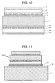
- FIG. 10 is a cross-sectional view showing another embodiment of a semiconductor power element heat dissipation board in accordance with the present invention.
- the board is formed by bonding the conductor plate 6 having the nickel plated film 7 formed on one surface and the diffusion suppression member 5 on the other surface and the heat sink plate 6a having the nickel plated film 7a formed on one surface and the diffusion suppression member 5a on the other surface onto both surfaces of the ceramic plate 1 using the aluminum alloy group solder members 4 and 4a, respectively.
- the conductor plate 6 and the heat sink plate 6a are formed of copper or a copper alloy, and the diffusion suppression member 5 and the diffusion suppression member 5a are formed of the same material as the above-mentioned material preventing diffusion of copper in the conductor plate 6 and in the heat sink plate 6a to aluminum in the aluminum alloy group solder members 4 and 4a or suppressing the effect of diffusion to the aluminum.
- the thickness of each of the diffusion suppression members is at least 5 ⁇ m or thicker in the case of pure nickel, and above several ⁇ m in the cases of the other materials.
- the thickness of the conductor plate 6 and the thickness of the heat sink plate 6a are nearly equal to each other and about several hundreds ⁇ m, respectively. In this embodiment, a high bonding strength can be also obtained, similarly to the cases described above.
- the aluminum alloy group solder members 4 and 4a can employ that shown in FIG. 3 (a), similarly to Embodiment 1.
- FIG. 11 is a cross-sectional view showing another embodiment of a semiconductor power element heat dissipation board in accordance with the present invention.
- the semiconductor power element heat dissipation board is formed by bonding the heat dissipation board portion assembly 300 onto the heat sink plate 1 having the nickel plated film 19 using the solder 20.
- the conductor plate 6 and the heat sink plate 6a in this figure are bonded by the aluminum alloy group solder members (the bonding temperature is as low as 580 to 610 °C), and accordingly, the thermal stress in the bonding portions is small compared to that of the conventional direct bonding method (the bonding temperature is above 1000 °C) of oxidizing the copper surface utilizing the eutectic of copper suboxide and copper or the conventional active metal solder method (the bonding temperature is about 850 °C).
- the bonding temperature is about 850 °C.
- FIG. 12 is an exploded cross-sectional view showing another embodiment of a semiconductor power element heat dissipation board in accordance with the present invention.
- a heat dissipation board portion assembly 400 is defined by an assembly which is formed by bonding the conductor plate 21 and the heat sink plate 22 each made of copper or an copper alloy on the both surfaces of the ceramic substrate 3 by the direct bonding method or the active metal solder method of the prior art, and then forming the nickel plated films 23, 24 on the surfaces of the conductor plate 21 and the heat sink plate 22, respectively.
- the semiconductor power element heat dissipation board is formed by bonding the heat dissipation board portion assembly 400 onto the heat sink plate 1 having a film of the diffusion suppression member 13 using the aluminum alloy group solder 2.
- the thickness of the conductor plate 21 and the thickness of the heat sink plate 22 are several hundreds ⁇ m, respectively. In this embodiment, a high bonding strength can be also obtained by the bonding using the aluminum alloy group solder, similarly to the cases described above. Further, the aluminum alloy group solder member 2 can employ that shown in FIG. 3 (a), similarly to Embodiment 1.
- FIG. 13 is a cross-sectional view showing another embodiment of a semiconductor power element heat dissipation board in accordance with the present invention.
- the semiconductor power element heat dissipation board is a board which is formed by bonding the conductor plate 6 having the nickel plated film 7 formed on one surface and the nickel plated film 27 on the other surface and the heat sink plate 1 having the nickel plated film 25 formed on one surface and the nickel plated film 26 on the other surface onto both surfaces of the ceramic plate 3 using the composite solder members having the aluminum alloy group solder portions 9 and 10 formed on the both surfaces of the core material portion 8 made of aluminum or an aluminum alloy.
- the aluminum alloy group solder portion (corresponds to the part indicated by the reference character 4 or 2 in FIG.
- the conductor plate 6 is made of a copper group material of copper or an copper alloy
- the heat sink plate 1 is made of a copper composite material.
- the thickness of the nickel plated films 27 and 25 was thicker than 10 ⁇ m and the time exposing high temperature at bonding was not a long period, these nickel plated films sufficiently functioned as the material for preventing copper in the conductor plate 6 and the heat sink plate 1 from diffusing into aluminum in the aluminum alloy group solder members 9 and 10 or for suppressing the effect of diffusion to the aluminum.
- the laminated body of the conductor plate 6, the ceramic plate 3 and the heat sink plate 1 was heated up to 610 °C and added with a load of 1 MPa through a pressing jig made of ceramic under a vacuum atmosphere or an inert atmosphere.
- the temperature was kept at610 °C for 10 minutes while the load was being added to the laminated body, and then the temperature was lowered, and the load was released at the time when the temperature of the laminated body became 300 °C.
- a 1000-cycle thermal shock endurance test of 40 to 150 °C was conducted using a semiconductor power element heat dissipation board manufactured under the above-mentioned bonding condition using the aluminum alloy group solder member having the total thickness (the total thickness of the solder portion 9/ the core material portion 8/ the solder portion 10) of 160 ⁇ m. As the result of the test, any trouble such as separation of the bonding portion did not occur.
- Test pieces were formed by bonding a copper plate or an aluminum plate to a ceramic (alumina, aluminum nitride or silicon nitride) plate using Al-12%Si alloy solder and adding a load of 1 MPa through the method described in this embodiment. As the result of test using the test pieces, bonding strengths above several tens MPa were obtained, and void (unbonded portion) in the bonding portions was nearly 0 %.
- the heat sink plate 1 made of the copper composite material of composite material (Cu/Cu 2 O) of copper (Cu) and cuprous oxide (Cu 2 O) has a property that cuprous oxide (Cu 2 O) in the material is likely reduced to copper (Cu) under a reducing atmosphere.
- the aluminum alloy group solders capable of bonding under a vacuum atmosphere or an inert atmosphere are bonding materials suitable for the copper composite material.
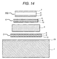
- FIG. 14 is an exploded cross-sectional view showing the semiconductor power element heat dissipation board of FIG. 13 before bonding.
- the conductor plate 6 having the nickel plated film 7 formed on one surface and the nickel plated film 27 formed on the other surface is indicated by the conductor plate portion assembly 500
- the aluminum alloy group solder members made of the laminated clad members of the solder portion 9/ the core material portion 8/ the solder portion 10 is indicated by the reference characters 4 and 2.
- the semiconductor power element heat dissipation board for example, shown in FIG. 13 is manufactured, the conductor plate portion assembly 500, the aluminum alloy group solder member 4, the ceramic plate 3, the aluminum alloy group solder member 2 and the heat sink plate 1 are laminated, and the laminated body is put between a jig 30 and a jig 29, as shown in FIG. 15, and then a load of 0.1 to 10 MPa is added to the laminated body under a high temperature of 580 to 610 °C.
- the amount of melted solder flowing out from the bonding portion is very small when the aluminum alloy group solder is formed in the clad member.
- the flatness of the conductor plate portion assembly 500 or the heat sink plate 1 is not so good or when an extraneous object exists in the laminating portion of the laminated body, there occurs a rare case that melted solder locally flows out to form a bridge 28 of the solder material shown in FIG. 15 between the conductor plate portion assembly 500 and the heat sink plate 1. In that case, a trouble of electric short circuit occurs between the conductor plate portion assembly 500 and the heat sink plate 1.
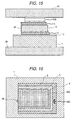
- FIG. 16 is a plan view showing a semiconductor power element heat dissipation board.
- the plane shape of the bridge of solder is indicated by the reference character 28.
- the short circuit trouble does not occur. If the melted solder locally flows out from a position between the ceramic plate 3 and the heat sink plate 1, the flowing-out melted solder flows along the surface of the aluminum alloy solder member 2. Therefore, the flowing-out melted solder does not form the vertical bridge which causes a short circuit between the conductor plate portion assembly 500 and the heat sink plate 1.
- a feature of the melted solder flow along the surface direction is schematically illustrated by arrows 600.
- a high bonding strength can be also obtained by using the aluminum alloy group solder members, similarly to the above-described embodiments.
- the present inventions described in FIG. 1 to FIG. 16 are the embodiments in the cases where the melting temperature of the aluminum alloy group solder material is about 580 °C, and the work temperature at bonding is as high as at least 500 °C or higher. Description will be made below on the present invention in the case where the melting temperature of the aluminum alloy group solder material is 400 °C, and the work temperature at bonding is as low as at least 500 °C or lower.
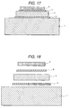
- FIG. 17 shows an embodiment of a semiconductor power element heat dissipation board in accordance with the present invention which uses the low temperature aluminum alloy group solder materials described above.
- the semiconductor power element heat dissipation board is formed by laminating the conductor plate 6 made of copper or a copper alloy, the ceramic plate 3 and the heat sink plate 1 made of copper or a copper alloy, and then bonding these plates using the aluminum alloy group solder material member 4 and 2. Even if a copper group material such as copper or a copper alloy or a copper composite material was employed for the conductor plate 6 and the heat sink plate 1 though there was no need to say the case of employing aluminum or an aluminum alloy, it was unnecessary to form the film of the diffusion suppression member for preventing diffusion of copper to aluminum in the aluminum alloy group solder or for suppressing the effect of diffusion to the aluminum.
- the work temperature at bonding is lower than the eutectic temperature (melting temperature) of aluminum and copper of 548 °C, the thickness of produced aluminum chemical compound (Al/Cu) can be made very thin even if the film of the diffusion suppression member is not formed. Further, since the work temperature at bonding is low temperature of 400 °C class, the productivity is improved and the residual thermal stress produced in the bonding portion is decreased to a very small value. Furthermore, by employing the laminated clad member of the solder portion/- the core material portion/ the solder portion to the aluminum alloy group solder material, a highly reliable semiconductor power element heat dissipation board without void in the bonding portion and having a high bonding strength could be obtained. In addition, the bonding strength and the state of void formation in this embodiment were similar to those in the above-mentioned embodiments.
- FIG. 18 is an exploded cross-sectional view showing the semiconductor power element heat dissipation board of FIG. 17 before bonding.
- a heat dissipation board having a very simple structure can be obtained.
- the semiconductor power element heat dissipation board according to the present invention When the semiconductor power element heat dissipation board according to the present invention is applied to a power module, the semiconductor power element is bonded onto the conductor plate 6 or 20 by solder though this has not been illustrated in the figure.
- the present invention there is the remarkable effect of obtaining a semiconductor power element heat dissipation board which has a high bonding strength without voids in the bonding portion, and has high reliability without forming a thick brittle Al/Cu intermetallic chemical compound, and of which the manufacturing method is simple, and to provide a conductor plate and a heat sink plate and a solder used for the semiconductor power element heat dissipation board, and to provide a power module and a composite plate using the semiconductor power element heat dissipation board.
Landscapes
- Cooling Or The Like Of Semiconductors Or Solid State Devices (AREA)
Applications Claiming Priority (4)
| Application Number | Priority Date | Filing Date | Title |
|---|---|---|---|
| JP2000332347 | 2000-10-31 | ||
| JP2000332347 | 2000-10-31 | ||
| JP2001033342A JP2002203932A (ja) | 2000-10-31 | 2001-02-09 | 半導体パワー素子用放熱基板とその導体板及びヒートシンク材並びにロー材 |
| JP2001033342 | 2001-02-09 |
Publications (1)
| Publication Number | Publication Date |
|---|---|
| EP1202345A2 true EP1202345A2 (de) | 2002-05-02 |
Family
ID=26603122
Family Applications (1)
| Application Number | Title | Priority Date | Filing Date |
|---|---|---|---|
| EP01125817A Withdrawn EP1202345A2 (de) | 2000-10-31 | 2001-10-29 | Leistungshalbleiterelement-Wärmeleitplatte, Leitplatte dafür, Kühlkörpermaterial und Lotmaterial |
Country Status (3)
| Country | Link |
|---|---|
| US (2) | US20020089828A1 (de) |
| EP (1) | EP1202345A2 (de) |
| JP (1) | JP2002203932A (de) |
Cited By (6)
| Publication number | Priority date | Publication date | Assignee | Title |
|---|---|---|---|---|
| EP1416533A2 (de) | 2002-10-29 | 2004-05-06 | Ixys Corporation | Leistungshalbleiter und Aluminium-direktgebondetes Substrat dafür |
| WO2008083853A1 (de) * | 2007-01-10 | 2008-07-17 | Osram Gesellschaft mit beschränkter Haftung | Elektronisches bauelementmodul und verfahren zu dessen herstellung |
| DE102009042518A1 (de) * | 2009-09-16 | 2011-03-24 | Esw Gmbh | Vorrichtung zur Kühlung von Halbleitern |
| CN106165087A (zh) * | 2014-04-25 | 2016-11-23 | 三菱综合材料株式会社 | 功率模块用基板、带散热片的功率模块用基板及带散热片的功率模块 |
| CN111357100A (zh) * | 2017-11-18 | 2020-06-30 | Jfe精密株式会社 | 散热板及其制造方法 |
| US20220362891A1 (en) * | 2019-10-08 | 2022-11-17 | Rogers Germany Gmbh | Method for producing a metal-ceramic substrate, solder system, and metal-ceramic substrate produced using such a method |
Families Citing this family (40)
| Publication number | Priority date | Publication date | Assignee | Title |
|---|---|---|---|---|
| WO2002067324A1 (en) * | 2001-02-22 | 2002-08-29 | Ngk Insulators, Ltd. | Member for electronic circuit, method for manufacturing the member, and electronic part |
| US7069645B2 (en) * | 2001-03-29 | 2006-07-04 | Ngk Insulators, Ltd. | Method for producing a circuit board |
| JP2003198116A (ja) * | 2001-12-28 | 2003-07-11 | Matsushita Electric Ind Co Ltd | はんだ付け方法および接合構造体 |
| US6905060B2 (en) * | 2003-10-24 | 2005-06-14 | The Boeing Company | Method and sealant for weld joints |
| US7532481B2 (en) * | 2004-04-05 | 2009-05-12 | Mitsubishi Materials Corporation | Al/AlN joint material, base plate for power module, power module, and manufacturing method of Al/AlN joint material |
| NL1027632C2 (nl) * | 2004-12-01 | 2006-06-02 | Electrische App Nfabriek Capax | Drager voor elektrische componenten met aangesoldeerd koellichaam. |
| US7521789B1 (en) * | 2004-12-18 | 2009-04-21 | Rinehart Motion Systems, Llc | Electrical assembly having heat sink protrusions |
| US7732033B2 (en) * | 2005-08-26 | 2010-06-08 | The Curators Of The University Of Missouri | Sealants for structural member joints and methods of using same |
| JP5128951B2 (ja) * | 2005-09-28 | 2013-01-23 | 日本碍子株式会社 | ヒートシンクモジュール及びその製造方法 |
| JP4916737B2 (ja) * | 2006-03-14 | 2012-04-18 | 三菱マテリアル株式会社 | 冷却器 |
| FR2899763B1 (fr) * | 2006-04-06 | 2008-07-04 | Valeo Electronique Sys Liaison | Support, notamment pour composant electronique de puissance, module de puissance comprenant ce support, ensemble comprenant le module et organe electrique pilote par ce module |
| EP2034520B1 (de) * | 2006-06-08 | 2013-04-03 | International Business Machines Corporation | Hochwärmeleitfähiges flexibles blatt |
| JP4748074B2 (ja) * | 2007-02-01 | 2011-08-17 | 三菱マテリアル株式会社 | パワーモジュール用基板、その製造方法、パワーモジュール |
| JP4964009B2 (ja) * | 2007-04-17 | 2012-06-27 | 株式会社豊田中央研究所 | パワー半導体モジュール |
| JP5070014B2 (ja) * | 2007-11-21 | 2012-11-07 | 株式会社豊田自動織機 | 放熱装置 |
| JP2009130060A (ja) * | 2007-11-21 | 2009-06-11 | Toyota Industries Corp | 放熱装置 |
| DE102008054415A1 (de) * | 2008-12-09 | 2010-06-10 | Robert Bosch Gmbh | Anordnung zweier Substrate mit einer SLID-Bondverbindung und Verfahren zur Herstellung einer solchen Anordnung |
| JP2010177413A (ja) * | 2009-01-29 | 2010-08-12 | Sumitomo Light Metal Ind Ltd | 発熱部品冷却装置用アルミニウム・クラッド材の製造方法 |
| JP2010177414A (ja) * | 2009-01-29 | 2010-08-12 | Sumitomo Light Metal Ind Ltd | 発熱部品冷却装置用アルミニウム・クラッド材 |
| JP5546889B2 (ja) * | 2010-02-09 | 2014-07-09 | 日本電産エレシス株式会社 | 電子部品ユニット及びその製造方法 |
| JP5466578B2 (ja) * | 2010-05-27 | 2014-04-09 | 株式会社神戸製鋼所 | ダイヤモンド・アルミニウム接合体及びその製造方法 |
| JP5832731B2 (ja) * | 2010-08-10 | 2015-12-16 | 株式会社東芝 | 半導体素子 |
| JP5705506B2 (ja) * | 2010-11-08 | 2015-04-22 | 昭和電工株式会社 | 絶縁基板用クラッド材 |
| US9735126B2 (en) * | 2011-06-07 | 2017-08-15 | Infineon Technologies Ag | Solder alloys and arrangements |
| JP5675525B2 (ja) * | 2011-07-28 | 2015-02-25 | 日産自動車株式会社 | 半導体装置の製造方法及び半導体装置 |
| JP5917903B2 (ja) * | 2011-12-19 | 2016-05-18 | 昭和電工株式会社 | ろう付用クラッド材 |
| JP5918008B2 (ja) * | 2012-05-08 | 2016-05-18 | 昭和電工株式会社 | 冷却器の製造方法 |
| JP5686128B2 (ja) * | 2012-11-29 | 2015-03-18 | トヨタ自動車株式会社 | 半導体装置 |
| CN103500787A (zh) * | 2013-10-16 | 2014-01-08 | 北京大学东莞光电研究院 | 一种底部可直接焊接于散热器的陶瓷cob封装led光源 |
| DE102014213490C5 (de) * | 2014-07-10 | 2020-06-18 | Continental Automotive Gmbh | Kühlvorrichtung, Verfahren zur Herstellung einer Kühlvorrichtung und Leistungsschaltung |
| EP3208839B1 (de) | 2014-10-16 | 2021-07-28 | Mitsubishi Materials Corporation | Substrat mit kühler für leistungsmodule und verfahren zur herstellung davon |
| JP6409621B2 (ja) * | 2015-03-03 | 2018-10-24 | 三菱マテリアル株式会社 | セラミックス基板とアルミニウム板との接合体の製造方法 |
| JP6531644B2 (ja) * | 2015-12-28 | 2019-06-19 | 三菱マテリアル株式会社 | 接合体の製造方法、ヒートシンク付パワーモジュール用基板の製造方法、接合体及びヒートシンク付パワーモジュール用基板 |
| CZ306788B6 (cs) * | 2016-07-14 | 2017-07-07 | Západočeská Univerzita V Plzni | Mezivrstva pro pájené spojení |
| JP6769169B2 (ja) * | 2016-08-22 | 2020-10-14 | 三菱マテリアル株式会社 | セラミックス基板とアルミニウム含浸炭化珪素多孔質体との接合体の製造方法 |
| JP6658400B2 (ja) * | 2016-08-24 | 2020-03-04 | 三菱マテリアル株式会社 | セラミックス/Al−SiC複合材料接合体の製造方法、及びヒートシンク付パワーモジュール用基板の製造方法 |
| CN108323137A (zh) * | 2017-01-18 | 2018-07-24 | 台达电子工业股份有限公司 | 均热板 |
| US11524359B2 (en) * | 2017-08-23 | 2022-12-13 | Georgia Tech Research Corporation | Low temperature direct bonding of aluminum nitride to AlSiC substrates |
| EP3753912A4 (de) * | 2018-02-14 | 2021-10-13 | Mitsubishi Materials Corporation | Verfahren zur herstellung eines verbundkörpers aus keramik/al-sic-verbundmaterial und verfahren zur herstellung eines mit einem kühlkörper ausgestatteten substrats für leistungsmodul |
| US11610861B2 (en) * | 2020-09-14 | 2023-03-21 | Infineon Technologies Austria Ag | Diffusion soldering with contaminant protection |
-
2001
- 2001-02-09 JP JP2001033342A patent/JP2002203932A/ja active Pending
- 2001-10-29 EP EP01125817A patent/EP1202345A2/de not_active Withdrawn
- 2001-10-31 US US09/984,974 patent/US20020089828A1/en not_active Abandoned
-
2002
- 2002-07-30 US US10/207,070 patent/US20020191378A1/en not_active Abandoned
Cited By (13)
| Publication number | Priority date | Publication date | Assignee | Title |
|---|---|---|---|---|
| EP1416533B1 (de) * | 2002-10-29 | 2016-04-27 | Ixys Corporation | Leistungshalbleiter und Aluminium-direktgebondetes Substrat dafür |
| EP1416533A2 (de) | 2002-10-29 | 2004-05-06 | Ixys Corporation | Leistungshalbleiter und Aluminium-direktgebondetes Substrat dafür |
| EP2317549A3 (de) * | 2002-10-29 | 2011-09-14 | Ixys Corporation | Direktgebondetes Substrat für Leistungshalbleiterbaulelement. |
| WO2008083853A1 (de) * | 2007-01-10 | 2008-07-17 | Osram Gesellschaft mit beschränkter Haftung | Elektronisches bauelementmodul und verfahren zu dessen herstellung |
| CN101548379B (zh) * | 2007-01-10 | 2011-01-12 | 奥斯兰姆有限公司 | 电子器件模块及其制造方法 |
| US8164177B2 (en) | 2007-01-10 | 2012-04-24 | Osram Ag | Electronic component module and method for production thereof |
| DE102009042518A1 (de) * | 2009-09-16 | 2011-03-24 | Esw Gmbh | Vorrichtung zur Kühlung von Halbleitern |
| CN106165087A (zh) * | 2014-04-25 | 2016-11-23 | 三菱综合材料株式会社 | 功率模块用基板、带散热片的功率模块用基板及带散热片的功率模块 |
| CN111357100A (zh) * | 2017-11-18 | 2020-06-30 | Jfe精密株式会社 | 散热板及其制造方法 |
| US11646243B2 (en) | 2017-11-18 | 2023-05-09 | Jfe Precision Corporation | Heat sink and method for manufacturing same |
| CN111357100B (zh) * | 2017-11-18 | 2023-09-01 | Jfe精密株式会社 | 散热板及其制造方法 |
| US20220362891A1 (en) * | 2019-10-08 | 2022-11-17 | Rogers Germany Gmbh | Method for producing a metal-ceramic substrate, solder system, and metal-ceramic substrate produced using such a method |
| US11945054B2 (en) * | 2019-10-08 | 2024-04-02 | Rogers Germany Gmbh | Method for producing a metal-ceramic substrate, solder system, and metal-ceramic substrate produced using such a method |
Also Published As
| Publication number | Publication date |
|---|---|
| JP2002203932A (ja) | 2002-07-19 |
| US20020089828A1 (en) | 2002-07-11 |
| US20020191378A1 (en) | 2002-12-19 |
Similar Documents
| Publication | Publication Date | Title |
|---|---|---|
| EP1202345A2 (de) | Leistungshalbleiterelement-Wärmeleitplatte, Leitplatte dafür, Kühlkörpermaterial und Lotmaterial | |
| CA2547358C (en) | Thermal interface material and solder preforms | |
| US7663242B2 (en) | Thermal interface material and solder preforms | |
| KR102224535B1 (ko) | 파워 모듈용 기판의 제조 방법 | |
| US6294828B1 (en) | Semiconductor chip package | |
| EP3041042B1 (de) | Verfahren zur herstellung eines verbundkörpers und verfahren zur herstellung eines strommodulsubstrats | |
| US5050040A (en) | Composite material, a heat-dissipating member using the material in a circuit system, the circuit system | |
| EP2234155B1 (de) | Verfahren zur Herstellung einer Halbleitervorrichtung | |
| US7355853B2 (en) | Module structure and module comprising it | |
| CN109755208B (zh) | 一种接合材料、半导体装置及其制造方法 | |
| WO2011027820A1 (ja) | 鉛フリーはんだ合金、接合用部材及びその製造法、並びに電子部品 | |
| JP4104253B2 (ja) | 基板一体型構造体 | |
| US7083759B2 (en) | Method of producing a heat dissipation substrate of molybdenum powder impregnated with copper with rolling in primary and secondary directions | |
| EP0365275B1 (de) | Kühlelement aus Verbundmaterial für ein Halbleiterbauelement und Herstellungsverfahren dafür | |
| JP2005503926A (ja) | 高温無鉛はんだに適した改良された組成物、方法およびデバイス | |
| JP2005032834A (ja) | 半導体チップと基板との接合方法 | |
| JPH06268117A (ja) | 半導体装置用放熱基板およびその製造方法 | |
| JP2002359425A (ja) | サブマウントおよび半導体装置 | |
| EP1553627A1 (de) | Material für eine wärmeabführende Platte, auf der ein Halbleiter montiert ist, und hieraus produziertes keramisches Gehäuse | |
| WO2011036829A1 (ja) | 半導体装置及びその製造方法 | |
| US20250391743A1 (en) | Multilayer assembly, semiconductor device using same, and method for manufacturing same | |
| US20050089700A1 (en) | Solder film manufacturing method, heat sink furnished with solder film, and semiconductor-device-and-heat-sink junction | |
| JPH0786444A (ja) | 半導体用複合放熱基板の製造方法 | |
| JP7267522B1 (ja) | 接合部材および半導体装置 | |
| KR20250078980A (ko) | 전자 부품 및 전자 부품의 제조 방법 |
Legal Events
| Date | Code | Title | Description |
|---|---|---|---|
| PUAI | Public reference made under article 153(3) epc to a published international application that has entered the european phase |
Free format text: ORIGINAL CODE: 0009012 |
|
| AK | Designated contracting states |
Kind code of ref document: A2 Designated state(s): AT BE CH CY DE DK ES FI FR GB GR IE IT LI LU MC NL PT SE TR |
|
| AX | Request for extension of the european patent |
Free format text: AL;LT;LV;MK;RO;SI |
|
| STAA | Information on the status of an ep patent application or granted ep patent |
Free format text: STATUS: THE APPLICATION HAS BEEN WITHDRAWN |
|
| 18W | Application withdrawn |
Effective date: 20040415 |