EP1416533B1 - Leistungshalbleiter und Aluminium-direktgebondetes Substrat dafür - Google Patents
Leistungshalbleiter und Aluminium-direktgebondetes Substrat dafür Download PDFInfo
- Publication number
- EP1416533B1 EP1416533B1 EP03011536.4A EP03011536A EP1416533B1 EP 1416533 B1 EP1416533 B1 EP 1416533B1 EP 03011536 A EP03011536 A EP 03011536A EP 1416533 B1 EP1416533 B1 EP 1416533B1
- Authority
- EP
- European Patent Office
- Prior art keywords
- substrate
- aluminum
- layer
- dab
- substrates
- Prior art date
- Legal status (The legal status is an assumption and is not a legal conclusion. Google has not performed a legal analysis and makes no representation as to the accuracy of the status listed.)
- Expired - Lifetime
Links
Images


Classifications
-
- H—ELECTRICITY
- H10—SEMICONDUCTOR DEVICES; ELECTRIC SOLID-STATE DEVICES NOT OTHERWISE PROVIDED FOR
- H10W—GENERIC PACKAGES, INTERCONNECTIONS, CONNECTORS OR OTHER CONSTRUCTIONAL DETAILS OF DEVICES COVERED BY CLASS H10
- H10W40/00—Arrangements for thermal protection or thermal control
- H10W40/20—Arrangements for cooling
- H10W40/25—Arrangements for cooling characterised by their materials
- H10W40/255—Arrangements for cooling characterised by their materials having a laminate or multilayered structure, e.g. direct bond copper [DBC] ceramic substrates
-
- H—ELECTRICITY
- H10—SEMICONDUCTOR DEVICES; ELECTRIC SOLID-STATE DEVICES NOT OTHERWISE PROVIDED FOR
- H10W—GENERIC PACKAGES, INTERCONNECTIONS, CONNECTORS OR OTHER CONSTRUCTIONAL DETAILS OF DEVICES COVERED BY CLASS H10
- H10W70/00—Package substrates; Interposers; Redistribution layers [RDL]
- H10W70/40—Leadframes
- H10W70/411—Chip-supporting parts, e.g. die pads
- H10W70/413—Insulating or insulated substrates serving as die pads
-
- H—ELECTRICITY
- H10—SEMICONDUCTOR DEVICES; ELECTRIC SOLID-STATE DEVICES NOT OTHERWISE PROVIDED FOR
- H10W—GENERIC PACKAGES, INTERCONNECTIONS, CONNECTORS OR OTHER CONSTRUCTIONAL DETAILS OF DEVICES COVERED BY CLASS H10
- H10W70/00—Package substrates; Interposers; Redistribution layers [RDL]
- H10W70/40—Leadframes
- H10W70/481—Leadframes for devices being provided for in groups H10D8/00 - H10D48/00
-
- H—ELECTRICITY
- H10—SEMICONDUCTOR DEVICES; ELECTRIC SOLID-STATE DEVICES NOT OTHERWISE PROVIDED FOR
- H10W—GENERIC PACKAGES, INTERCONNECTIONS, CONNECTORS OR OTHER CONSTRUCTIONAL DETAILS OF DEVICES COVERED BY CLASS H10
- H10W70/00—Package substrates; Interposers; Redistribution layers [RDL]
- H10W70/60—Insulating or insulated package substrates; Interposers; Redistribution layers
- H10W70/62—Insulating or insulated package substrates; Interposers; Redistribution layers characterised by their interconnections
- H10W70/65—Shapes or dispositions of interconnections
- H10W70/658—Shapes or dispositions of interconnections for devices provided for in groups H10D8/00 - H10D48/00
-
- H—ELECTRICITY
- H10—SEMICONDUCTOR DEVICES; ELECTRIC SOLID-STATE DEVICES NOT OTHERWISE PROVIDED FOR
- H10W—GENERIC PACKAGES, INTERCONNECTIONS, CONNECTORS OR OTHER CONSTRUCTIONAL DETAILS OF DEVICES COVERED BY CLASS H10
- H10W70/00—Package substrates; Interposers; Redistribution layers [RDL]
- H10W70/60—Insulating or insulated package substrates; Interposers; Redistribution layers
- H10W70/67—Insulating or insulated package substrates; Interposers; Redistribution layers characterised by their insulating layers or insulating parts
- H10W70/68—Shapes or dispositions thereof
- H10W70/685—Shapes or dispositions thereof comprising multiple insulating layers
-
- H—ELECTRICITY
- H10—SEMICONDUCTOR DEVICES; ELECTRIC SOLID-STATE DEVICES NOT OTHERWISE PROVIDED FOR
- H10W—GENERIC PACKAGES, INTERCONNECTIONS, CONNECTORS OR OTHER CONSTRUCTIONAL DETAILS OF DEVICES COVERED BY CLASS H10
- H10W72/00—Interconnections or connectors in packages
- H10W72/50—Bond wires
- H10W72/541—Dispositions of bond wires
- H10W72/5449—Dispositions of bond wires not being orthogonal to a side surface of the chip, e.g. fan-out arrangements
-
- H—ELECTRICITY
- H10—SEMICONDUCTOR DEVICES; ELECTRIC SOLID-STATE DEVICES NOT OTHERWISE PROVIDED FOR
- H10W—GENERIC PACKAGES, INTERCONNECTIONS, CONNECTORS OR OTHER CONSTRUCTIONAL DETAILS OF DEVICES COVERED BY CLASS H10
- H10W72/00—Interconnections or connectors in packages
- H10W72/50—Bond wires
- H10W72/541—Dispositions of bond wires
- H10W72/547—Dispositions of multiple bond wires
- H10W72/5475—Dispositions of multiple bond wires multiple bond wires connected to common bond pads at both ends of the wires
-
- H—ELECTRICITY
- H10—SEMICONDUCTOR DEVICES; ELECTRIC SOLID-STATE DEVICES NOT OTHERWISE PROVIDED FOR
- H10W—GENERIC PACKAGES, INTERCONNECTIONS, CONNECTORS OR OTHER CONSTRUCTIONAL DETAILS OF DEVICES COVERED BY CLASS H10
- H10W72/00—Interconnections or connectors in packages
- H10W72/50—Bond wires
- H10W72/551—Materials of bond wires
- H10W72/552—Materials of bond wires comprising metals or metalloids, e.g. silver
- H10W72/5524—Materials of bond wires comprising metals or metalloids, e.g. silver comprising aluminium [Al]
-
- H—ELECTRICITY
- H10—SEMICONDUCTOR DEVICES; ELECTRIC SOLID-STATE DEVICES NOT OTHERWISE PROVIDED FOR
- H10W—GENERIC PACKAGES, INTERCONNECTIONS, CONNECTORS OR OTHER CONSTRUCTIONAL DETAILS OF DEVICES COVERED BY CLASS H10
- H10W74/00—Encapsulations, e.g. protective coatings
-
- H—ELECTRICITY
- H10—SEMICONDUCTOR DEVICES; ELECTRIC SOLID-STATE DEVICES NOT OTHERWISE PROVIDED FOR
- H10W—GENERIC PACKAGES, INTERCONNECTIONS, CONNECTORS OR OTHER CONSTRUCTIONAL DETAILS OF DEVICES COVERED BY CLASS H10
- H10W90/00—Package configurations
- H10W90/701—Package configurations characterised by the relative positions of pads or connectors relative to package parts
- H10W90/751—Package configurations characterised by the relative positions of pads or connectors relative to package parts of bond wires
- H10W90/756—Package configurations characterised by the relative positions of pads or connectors relative to package parts of bond wires between a chip and a stacked lead frame, conducting package substrate or heat sink
Definitions
- This invention relates to electronic devices and components thereof, and more particularly to packaged power semiconductor devices and direct-bonded metal substrates thereof.
- Power semiconductor devices or power devices are designed to operate at relatively high voltages, typically 30-1,000 volts or higher.
- Many power devices such as, silicon-controlled rectifiers (“SCRs”), power transistors, insulated-gate bipolar transistors (“IGBTs”), metal-oxide-semiconductor field-effect transistors (“MOSFETs”), power rectifier, power regulators, or combinations thereof, are assembled in packages that are not electrically isolated. That is, a metal tab, which typically forms the backside of the packaged device, is electrically coupled, e.g. soldered, to the semiconductor die within the packaged device. This places the backside of the package at the same electrical potential as the semiconductor die.
- Heatsinking is important for power semiconductor devices because of the power dissipated by some devices during operation, and also because of the environment that the device may have to operate in. Power semiconductor devices are often used in applications that may get relatively hot, such as in an engine compartment or in a factory. Thus, it is especially important to minimize the thermal resistance between the active device, which may be generating several Watts or even several kilowatts of power, and the environment, which may be at an elevated temperature. Accordingly, a power semiconductor device preferably should have good thermal conductivity and reliable electrical isolation between the backside of the packaged power device and the semiconductor.
- One method used to provide such a power device is to manufacture a power device on a substrate having two conductive layers separated by a dielectric layer.
- EP 0 422 558 A2 discloses a ceramic substrate for an electric or electronic circuit.
- the ceramic substrate comprises a ceramic plate formed of a substance mainly composed of aluminum nitride, and conductive islands formed of aluminum or an aluminum alloy and bonded to one surface of said ceramic plate for providing conductive paths to circuit components connected thereto, wherein the aluminum or aluminum-alloy islands decrease the total weight of the ceramic substrate and enhance a resistance against repetition of a thermal stress.
- US 4 483 810 A discloses a method for the direct joining of metal pieces which have a surface metal oxide layer, to oxide ceramic substrates by heating the ceramic substrates covered with the metal pieces in an oxygen-containing atmosphere to a temperature above the eutectic temperature of the metal and the metal oxide, but below the melting temperature of the metal.
- US 6 404 065 B1 discloses a direct-bonded copper ("DBC") substrate to provide electrical isolation and good thermal transfer from the device to a heatsink.
- a power semiconductor die is soldered or otherwise mounted to a first metal layer of the DBC substrate.
- the first metal layer spreads heat generated by the semiconductor die.
- US 5 527 620 A discloses a metal coated substrate.
- a metal layer is attached to an insulating layer having a thickness of 0.2 mm. The metal layer is formed in a border area and is weakened by openings disposed in two rows.
- DE 4 004 844 C1 discloses a ceramic substrate with a structured Cu metallization.
- the ceramic substrate is produced by a process in which a Cu foil is bonded directly to the whole surface of the substrate and is then masked and etched. From the document JP 1 059 986 A a method for producing a ceramic circuit board which has an improved reliability for thermal hysteresis is known.
- the ceramic circuit board is produced by a DBC method wherein copper plates with required shapes are provided and bonded to the ceramic board and thin parts are formed along the ends of the copper plates.
- EP 1 202 345 A2 discloses a semiconductor power element heat dissipation board which has a high bonding strength without voids in the bonding portion without forming a thick brittle Al/Cu intermetallic chemical compound.
- EP 1 089 334 A2 provides a ceramic circuit board comprising: a ceramic substrate and a metal circuit plate bonded to the ceramic substrate through a brazing material layer; wherein the brazing material layer is composed of Al-Si group brazing material and an amount of Si contained in the brazing material is 7 wt% or less.
- a method for manufacturing a power semiconductor device comprises inserting a substrate assembly into a furnace having a plurality of process zones.
- the substrate assembly includes a first aluminum layer and a second aluminum layer that are electrically isolated from each other by a dielectric layer.
- the method further comprises providing the substrate assembly successively into each of the plurality of process zones to bond the first and second aluminum layers to the dielectric layer and obtain a direct bonded aluminum (DAB) substrate.
- DAB direct bonded aluminum
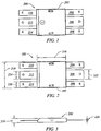
- the device includes three types of leads, all having blade-like shapes in one embodiment of the present invention.
- the leads of first type the leads 204, 208, 210, and 214, are coupled to source regions of the semiconductor die (not shown) within the package 202. Each lead has a width 220 ranging from about 0.1 to 0.17 inch (2.54 to 4.32 mm).
- the lead of second type, the lead 206 is coupled to a drain region and has a width 222 ranging from about 0.125 to 0.346 inch (3.175 to 8.79 mm).
- the lead of third type, the lead 212 is coupled to a gate and has a width 224 ranging from about 0.085 to 0.306 inch (2.16 to 7.77 mm).
- These leads 204-214 generally have a thickness 226 ranging from about 0.001 to 0.015 inch (0.025 to 0.38 mm). It one embodiment, the leads 204, 208, 210, and 214 have the width 220 of about 0.162 inch (4.115 mm). The lead 206 has the width 222 of about 0.346 inch (8.79 mm). The lead 212 has the width 224 of about 0.306 inch (7.77 mm). All of these leads have substantially the same thickness 226 of about 0.006 inch (0.152 mm). Accordingly, in this embodiment, the ratio of width to thickness for the leads 204, 208, 210, and 214 with the smallest width is 27, i.e., the width is 27 times greater than the thickness.
- the ratio of width to thickness is greater (e.g., 30, 35, or 40) or smaller (e.g., 20, 15, or 10) than 27.
- Fig. 4A depicts a top plan view of the device 200 with the plastic package 202 delayered as indicated by the dotted line.
- Fig. 4B depicts a cross sectional view of the device 200 with the plastic package 202 delayered as indicated by the dotted line. As shown, in Fig. 4B , the backside of the package 202 is flush with the backside of a DAB substrate.
- Fig. 5 depicts a top plan view of a direct bonded aluminum (DAB) substrate 228 of the device 200
- Fig. 6 depicts a cross sectional view of the DAB substrate 228.
- DAB direct bonded aluminum
- Various conductive regions are electrically coupled to the leads via wires 268 extending from the die to the leads.
- the wires 268 are aluminum wires but other conductive wires may be used. Bonding the leads to the blocks of the first aluminum layer 230, as shown in Fig. 4 , facilitates manufacturing of a plurality of the devices 200 in a single assembly process.
- the power device 200 with a DAB substrate 228 tends to provide greater structural integrity.
- the substrate or pad, on which the semiconductor die is provided, is less likely to crack because the composite DAB structure provides support for the ceramic layer.
- the power device 200 includes a direct bonded copper (DCB) substrate rather than a direct bonded aluminum substrate.
- DCB substrate generally is provided with an aluminum-based ceramic as the dielectric layer that is bonded to two conductive (or copper) layers in a controlled oxidizing ambient
- the DCB substrate has good thermal conductivity, good voltage isolation between the metal layers, good thermal ruggedness (the material keeps its properties over a wider temperature range than polymer based or glued metallic substrates like PCB and IMS), and similar thermal expansion coefficient as that of silicon or other semiconductor materials.
- thermal cycling a power semiconductor is subjected to cycles repeated between a low temperature state to a high temperature state without powering the device on.
- the said power device In power cycling the said power device is powered on and off, and its thermal excursion between these states is due to its self-heating.
- a combined thermal and power cycling is performed on the devices to test their reliability in accelerated testing.
- the power devices are subjected to such cycles in any combinations.
- the temperature operating range can be from -55C to +150C. In some other applications the temperature range can be even more severe while power is being applied to the device. Under such extreme circumstances, the power devices having DCB substrates have demonstrated structural failures.
- a variety of cracks start to form in the bonded areas between the copper and the ceramic layers, which propagate with each successive power cycle or thennal cycle, or both. At times micro-cracks are formed on the DCB substrate even during its manufacturing process, e.g., during a cooling period of the DCB substrate after a high temperature manufacturing step. These cracks lead to the structural and eventual electrical failure of such power devices in said applications.
- One solution to the above crack formation problem is to use a different bonded substrate technology, e.g., using an aluminum layer rather than a copper layer.
- the manufacturing process of the DAB substrate has to be customized due to the unique metallurgical and surface qualities of aluminum (A1).
- One process method used for manufacturing the DAB substrate involves performing the bonding a vacuum environment, requiring a two-step bonding process.
- the upper and lower aluminum layers are bonded to the dielectric layer in separate bonding steps. These two steps require at least two operations of breaking the vacuum in a suitable vacuum oven and then re-establishing the vacuum, before exposing the material for bonding in a high temperature process. Accordingly, the production output per hour is thus reduced when compared to a belt furnace operation, which provides a continuous bonding process.
- More detailed descriptions of the belt furnace operation used in manufacturing a direct bonded metal substrate can be found in, for example, EP 422,558 , and U.S. Patent No. 4,483,810 . Referring to Figs.
- the Al plate has a layer of an Al-Si alloy on one of its sides that is to be bonded to the ceramic or dielectric substrate.
- the Al-Si alloy has a Si concentration of less than about 15%, preferably less than about 11.7%, and more preferably less than about 8%. In one embodiment, the Si concentration is about 7.5% or 6.5%.
- the Al-Si layer has a lower melting point than pure Al, thereby enabling the bonding process to be conducted in a lower temperature.
- the thickness of the Al-Si alloy layer, provided on the Al "carrier" plate is preferably less than about 70 ⁇ m, or preferably less than about 50 ⁇ m according to one embodiment of the present invention.
- the total thickness of the aluminum plate including the Al-Si alloy is between about 150 ⁇ m and about 700 ⁇ m, or preferably between about 200 ⁇ m and about 500 ⁇ m.
- Fig. 10 shows an exemplary aluminum plate 612 having an Al-Si alloy layer 614 that is described above.
- the aluminum and ceramic substrates travels along one or more heating zones to be bonded. Generally, there are at least three heating zones in the furnace: (1) a preheating zone to gradually ramp up the temperature of the substrate assembly, (2) a primary heating zone to bring the substrate assembly to a temperature between eutectic and melting temperature of aluminum, and (3) a cooling zone to gradually cool the substrate assembly and solidify the eutectic melt.
- the solidification of the eutectic melt does not occur instantaneously, and the bonding process is not completed until the temperature drops well below the eutectic temperature.
- the cooling process generally may involve two or more steps to gradually ramp down the temperature during a period of about 15 minutes or more. Accordingly, the cooling zone may include two or more sub-zones. Other heating zones may include two or more sub-zones as well.
- An inert gas e.g., nitrogen
- gases are not present or are ⁇ 1 ppm.
- the belt furnace provides a continuous flow process where the substrate assembly travels on a metal conveyer belt of the furnace from one heating zone to another. In such a process, each substrate experiences the same heating zone and same temperature profile in contrast to a process involving separate bonding steps for the upper and lower aluminum layers. Accordingly, the belt furnace process provides a high throughput and requires less manufacturing cost.
- one or more weights are used to facilitate the bonding between the aluminum and ceramic substrates. Two weights are used, a top boat 602 and a bottom boat 604 ( Fig. 11 ), together they comprise the carrier 600 described above.
- the top boat 602 is placed on the upper aluminum substrate to apply a pressure to facilitate bonding, and the bottom boat 604 is placed below the lower aluminum substrate to isolate the bottom aluminum substrate from the metal belt of the furnace.
- the bottom boat is made of graphite that has relatively good thermal conductivity, relatively low mass and low thermal capacity.
- the top and bottom boats are made of graphite which does not easily interact chemically with the aluminum substrate or the metal alloys of the furnace belt. Referring back to Fig. 9 , the top boat 602 and the bottom boat 604 have substantially the same width a and length b according to one embodiment of the present invention.
- the width a is 14.22 cm (5.6 ") and the length b is 19.56 cm (7.7 ") in order to fit on ceramic and corresponding Al-AlSi plates of same or similar size.
- the top boat 602 weighs more than the bottom boat 604.
- the top boat 602 weighs more than the bottom boat 604.
- the top boat weighs 490 g and has a thickness of about 10 mm
- the bottom boat 604 weighs 245 g and has a thickness of about 5 mm.
- Fig. 13 illustrates the substrate assembly as it is aligned and conveyed on the belt through the furnace for bonding.
- graphite as a material for the boats is its ability to "getter” any traces of oxygen in the ambient above and around said belt in the furnace, especially through its "hot zones", and thus preventing the oxidation of the Al and AlSi alloy. Any such oxidation hinders proper bonding of the Al-AlSi substrate to the ceramic substrate.
- the top and bottom graphite boats act also as good heat spreaders spreading the heat in the furnace evenly over the surfaces of the substrate assembly due to graphite's superior thermal conductivity.
- the etch process is performed using the base of FeCl 3 chemistry or CuCl 2 chemistry that are used in an etch process for patterning a direct bonded copper (DCB) substrate.
- This type of etch process is used in order to combine the manufacturing of DCB and DAB substrates in the same production line, so that the need for re-tooling the equipment for DAB etch process is avoided.
- Residues of AlSi alloy remaining on the aluminum substrates after the etch or patterning step is removed by an nitric acid etchant (containing hydrofluoric and acetic acid), which has a high AlSi alloy etch selectivity, i.e., Al is not easily etched.
- the DAB substrate under goes a preferably selective electroless Ni- or Ni-/Au-plating process to prepare the DAB substrate or the bonded substrate assembly to adapt it to be suitably solderable (step 310).
- the plating is performed in the present embodiment because Al generally does not effectively wet conventional soft solders. Good solderability facilitates the use of the DAB substrate in electronic devices.
- the plating process is performed after zincate pre-treatment of the surface of the aluminum substrate.
- the phosphorous content of the nickel layer is about 6% to about 10%, preferably about 8%.
- the thickness of the nickel layer formed has about 3 ⁇ m to about 8 ⁇ m, preferably about 5 ⁇ m.
- the nickel layer is sufficiently thick enough to prevent solder penetration to the Ni-Al interface during the soldering process. Otherwise, the solder may not probably wet the contacting Al surface.
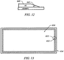
- the stress relief technique involves shaping the geometry of the edges of the aluminum layer to be bonded to the ceramic layer. Alternatively, the shaping may be performed during the patterning step after the bonding step, as with other stress relief techniques described herein.
- the edges of the metal layer 640 are provided with a grading slope 643 of degrees " ⁇ " ( Fig. 12 ) that is smaller than 90 degrees.
- the slope 643 has a degree between about 30 degrees to about 60 degrees.
- the metal layer is etched to provide a plurality of notches, holes, grooves, or bays at the edges of a metal substrate.
- Fig. 13 shows a metal substrate 650 including a plurality of notches 652 at edges thereof and a ceramic substrate 654 provided therebeneath.
- Fig. 14 shows an enlarged view of an edge portion 653 of the metal substrate 650 wherein the notches 652 are provided.
- the notches 652 have a pitch of 0.8 mm, a width of 0.2 mm, and a depth of 0.25 mm. Referring to Fig.
- the edge portion 653 includes a combination of variously-shaped notches along the edges of the metal layer 650 and having a sloping edge.
- a plurality of holes 656 of various shapes and diameters are etched in the metal layer for stress relief, i.e., to enhance stress-handling characteristics.
- the holes will cover the edge area up to a distance d (typically up to about 1 mm, depending on metal thickness) from the area of the edge with said notches.
- the combination of circular holes and notches as an example of one of many possibilities in achieving the desired stress relief pattern.
- the present stress relief techniques may be applied to various metal layers or substrates (e.g., aluminum or copper) used in forming a direct bonded metal substrates.
- stress relief techniques which do not relate to DAB substrates, do not form part of the present invention. While the invention has been particularly shown and described with reference to a specific embodiment thereof, it will be understood by those skilled in the art that the foregoing and other changes in the form and details may be made therein.
Landscapes
- Cooling Or The Like Of Semiconductors Or Solid State Devices (AREA)
- Internal Circuitry In Semiconductor Integrated Circuit Devices (AREA)
Claims (8)
- Verfahren zum Ausbilden eines direkt gebondeten Aluminiumsubstrats zur Verwendung in einem Leistungshalbleiterbauelement (200), wobei das Verfahren umfasst:Einsetzen einer Substratanordnung in einen Ofen mit einer Vielzahl von Prozesszonen, wobei die Substratanordnung ein erstes Aluminiumsubstrat und ein zweites Aluminiumsubstrat umfasst, die durch ein dielektrisches Substrat elektrisch voneinander isoliert sind, wobei das erste Aluminiumsubstrat und das zweite Aluminiumsubstrat jeweils mit einer Al-Si-Legierung oder einer Al-Mg-Legierung gegenüber dem dielektrischen Substrat beschichtet sind, wobei ein oberes Schiffchen (602) auf dem oberen Aluminiumsubstrat angeordnet wird undein unteres Schiffchen (604) unter dem unteren Aluminiumsubstrat angeordnet wird,wobei das obere Schiffchen (602) mehr wiegt als das untere Schiffchen (604) und wobei das obere Schiffchen (602) und das untere Schiffchen (604) aus Graphit bestehen, undZuführen der Substratanordnung nacheinander in jede der Vielzahl von Prozesszonen, um das erste und das zweite Aluminiumsubstrat an das dielektrische Substrat gleichzeitig zu bonden, wodurch ein direkt gebondetes Aluminium- (DAB) Substrat erhalten wird,wobei die Vielzahl von Prozesszonen umfasst:- eine Vorheizzone, um die Temperatur der Substratanordnung allmählich zu erhöhen,- eine primäre Heizzone, um die Substratanordnung auf eine Temperatur zwischen einer eutektischen Temperatur der Al-Si- oder Al-Mg-Legierung und der Schmelztemperatur von Aluminium zu bringen, und- eine Kühlzone, um die Substratanordnung allmählich zu kühlen und die eutektische Schmelze zu verfestigen,wobei ein Inertgas in die primäre Heiz- und die Kühlzone des Ofens geleitet wird, um das Bonden der Aluminiumsubstrate an das dielektrische Substrat zu erleichtern, ohne eine Vakuumumgebung bereitzustellen.
- Verfahren nach Anspruch 1, das ferner umfasst:Formen einer Kante von mindestens einem der Aluminiumsubstrate, um die Spannungshandhabungseigenschaften des DAB-Substrats zu verbessern.
- Verfahren nach Anspruch 2, wobei der Formungsschritt vor dem Bonden der Aluminiumsubstrate an das dielektrische Substrat durchgeführt wird.
- Verfahren nach Anspruch 2 oder 3, wobei das Formen an allen Außenkanten des einen der Aluminiumsubstrate durchgeführt wird.
- Verfahren nach einem der Ansprüche 2 bis 4, wobei der Formungsschritt umfasst:Vorsehen einer Neigung (643) an der Kante des mindestens einen der Aluminiumsubstrate, wobei die Neigung (643) einen Winkel von etwa 30 Grad bis etwa 60 Grad aufweist; undAusbilden einer Vielzahl von Kerben (652), Löchern (656) oder Nuten an der Kante des mindestens einen der Aluminiumsubstrate.
- Verfahren nach einem der vorangehenden Ansprüche,
wobei das erste und das zweite Aluminiumsubstrat eine erste und eine zweite Aluminiumschicht (230, 234) sind und das dielektrische Substrat eine dielektrische Schicht (232) ist. - Verfahren zur Herstellung eines Leistungshalbleiterbauelements, das umfasst:Ausbilden eines direkt gebondeten Aluminium- (DAB) Substrats, wie in Anspruch 6 definiert;Befestigen eines Halbleiterchips (266) an der ersten Aluminiumschicht (230) des DAB-Substrats; undAusbilden einer Umhüllung um den Halbleiterchip (266) und das DAB-Substrat, während ein beträchtlicher Abschnitt der zweiten Aluminiumschicht (234) für eine verstärkte Wärmeableitung freigelegt wird.
- Verfahren nach Anspruch 7, wobei die zweite Aluminiumschicht (234) mit einer Rückseite der Umhüllung bündig ist.
Priority Applications (1)
| Application Number | Priority Date | Filing Date | Title |
|---|---|---|---|
| EP10184009A EP2317549A3 (de) | 2002-10-29 | 2003-05-21 | Direktgebondetes Substrat für Leistungshalbleiterbaulelement. |
Applications Claiming Priority (2)
| Application Number | Priority Date | Filing Date | Title |
|---|---|---|---|
| US283829 | 2002-10-29 | ||
| US10/283,829 US6670216B2 (en) | 2001-10-31 | 2002-10-29 | Method for manufacturing a power semiconductor device and direct bonded substrate thereof |
Related Child Applications (1)
| Application Number | Title | Priority Date | Filing Date |
|---|---|---|---|
| EP10184009A Division-Into EP2317549A3 (de) | 2002-10-29 | 2003-05-21 | Direktgebondetes Substrat für Leistungshalbleiterbaulelement. |
Publications (3)
| Publication Number | Publication Date |
|---|---|
| EP1416533A2 EP1416533A2 (de) | 2004-05-06 |
| EP1416533A3 EP1416533A3 (de) | 2005-12-28 |
| EP1416533B1 true EP1416533B1 (de) | 2016-04-27 |
Family
ID=32093510
Family Applications (2)
| Application Number | Title | Priority Date | Filing Date |
|---|---|---|---|
| EP10184009A Ceased EP2317549A3 (de) | 2002-10-29 | 2003-05-21 | Direktgebondetes Substrat für Leistungshalbleiterbaulelement. |
| EP03011536.4A Expired - Lifetime EP1416533B1 (de) | 2002-10-29 | 2003-05-21 | Leistungshalbleiter und Aluminium-direktgebondetes Substrat dafür |
Family Applications Before (1)
| Application Number | Title | Priority Date | Filing Date |
|---|---|---|---|
| EP10184009A Ceased EP2317549A3 (de) | 2002-10-29 | 2003-05-21 | Direktgebondetes Substrat für Leistungshalbleiterbaulelement. |
Country Status (2)
| Country | Link |
|---|---|
| US (2) | US6670216B2 (de) |
| EP (2) | EP2317549A3 (de) |
Families Citing this family (31)
| Publication number | Priority date | Publication date | Assignee | Title |
|---|---|---|---|---|
| US20040094828A1 (en) * | 2002-01-16 | 2004-05-20 | Delphi Technologies, Inc. | Double-sided multi-chip circuit component |
| US6812553B2 (en) * | 2002-01-16 | 2004-11-02 | Delphi Technologies, Inc. | Electrically isolated and thermally conductive double-sided pre-packaged component |
| JP3935037B2 (ja) * | 2002-09-30 | 2007-06-20 | Dowaホールディングス株式会社 | アルミニウム−セラミックス接合基板の製造方法 |
| JP2005197688A (ja) * | 2003-12-29 | 2005-07-21 | Siemens Ag | 電子ユニット |
| JP4543279B2 (ja) * | 2004-03-31 | 2010-09-15 | Dowaメタルテック株式会社 | アルミニウム接合部材の製造方法 |
| US7045885B1 (en) | 2004-12-09 | 2006-05-16 | Hewlett-Packard Development Company, L.P. | Placement of absorbing material in a semiconductor device |
| EP1858078A4 (de) | 2005-01-20 | 2009-03-04 | Almt Corp | Element für ein halbleiterbauteil und herstellungsverfahren dafür |
| US7229855B2 (en) * | 2005-02-23 | 2007-06-12 | Delphi Technologies, Inc. | Process for assembling a double-sided circuit component |
| JP2006278913A (ja) * | 2005-03-30 | 2006-10-12 | Toyota Motor Corp | 回路装置とその製造方法 |
| US7745930B2 (en) * | 2005-04-25 | 2010-06-29 | International Rectifier Corporation | Semiconductor device packages with substrates for redistributing semiconductor device electrodes |
| CA2612866A1 (en) * | 2005-05-11 | 2006-11-23 | Corium International, Inc. | Permeabilization of biological membranes |
| US20070152321A1 (en) * | 2005-12-29 | 2007-07-05 | Wei Shi | Fluxless heat spreader bonding with cold form solder |
| US8435802B2 (en) * | 2006-05-22 | 2013-05-07 | Taiwan Semiconductor Manufacturing Co., Ltd. | Conductor layout technique to reduce stress-induced void formations |
| DE102009008637B4 (de) * | 2009-02-12 | 2022-05-12 | Ledvance Gmbh | Leuchtvorrichtung |
| US8034666B2 (en) * | 2009-11-15 | 2011-10-11 | Microsemi Corporation | Multi-layer thick-film RF package |
| US8841540B2 (en) | 2011-08-03 | 2014-09-23 | Marlow Industries, Inc. | High temperature thermoelectrics |
| TWI502709B (zh) | 2011-08-26 | 2015-10-01 | 光頡科技股份有限公司 | Metallographic Ceramic Plate Method |
| US20130139866A1 (en) * | 2011-12-01 | 2013-06-06 | Marlow Industries, Inc. | Ceramic Plate |
| WO2013136895A1 (ja) | 2012-03-15 | 2013-09-19 | 富士電機株式会社 | 半導体装置 |
| US8716864B2 (en) | 2012-06-07 | 2014-05-06 | Ixys Corporation | Solderless die attach to a direct bonded aluminum substrate |
| US8586480B1 (en) * | 2012-07-31 | 2013-11-19 | Ixys Corporation | Power MOSFET having selectively silvered pads for clip and bond wire attach |
| US8575767B1 (en) | 2012-10-06 | 2013-11-05 | Ixys Corporation | Reflow of thermoplastic sheet for passivation of power integrated circuits |
| JP6099453B2 (ja) * | 2012-11-28 | 2017-03-22 | Dowaメタルテック株式会社 | 電子部品搭載基板およびその製造方法 |
| US9496214B2 (en) * | 2013-05-22 | 2016-11-15 | Toyota Motor Engineering & Manufacturing North American, Inc. | Power electronics devices having thermal stress reduction elements |
| DE102014216845A1 (de) * | 2014-08-25 | 2016-02-25 | Conti Temic Microelectronic Gmbh | Schaltungsträger, Verfahren zur Herstellung eines Schaltungsträgers und Verwendung des Schaltungsträgers |
| DE102014220650A1 (de) | 2014-10-13 | 2016-04-14 | Heraeus Deutschland GmbH & Co. KG | Optimiertes Leiterbahndesign von metallischen Materialien auf keramischen Substanzen |
| US9443792B1 (en) | 2015-10-31 | 2016-09-13 | Ixys Corporation | Bridging DMB structure for wire bonding in a power semiconductor device module |
| US10000423B1 (en) | 2016-03-31 | 2018-06-19 | Ixys, Llc | Direct metal bonding on carbon-covered ceramic contact projections of a ceramic carrier |
| CN110556349B (zh) * | 2019-09-29 | 2024-09-24 | 全球能源互联网研究院有限公司 | 功率型半导体器件封装结构 |
| DE102022129493A1 (de) * | 2022-11-08 | 2024-05-08 | Rogers Germany Gmbh | Metall-Keramik-Substrat und Verfahren zur Herstellung von Metall-Keramik-Substraten |
| CN116180079B (zh) * | 2023-03-15 | 2024-01-23 | 江苏富乐华半导体科技股份有限公司 | 一种解决覆铜陶瓷载板高温下瓷片裂纹的方法 |
Citations (2)
| Publication number | Priority date | Publication date | Assignee | Title |
|---|---|---|---|---|
| EP1089334A2 (de) * | 1999-09-28 | 2001-04-04 | Kabushiki Kaisha Toshiba | Keramikleiterplatte |
| EP1202345A2 (de) * | 2000-10-31 | 2002-05-02 | Hitachi, Ltd. | Leistungshalbleiterelement-Wärmeleitplatte, Leitplatte dafür, Kühlkörpermaterial und Lotmaterial |
Family Cites Families (9)
| Publication number | Priority date | Publication date | Assignee | Title |
|---|---|---|---|---|
| DE3204167A1 (de) * | 1982-02-06 | 1983-08-11 | Brown, Boveri & Cie Ag, 6800 Mannheim | Verfahren zum direkten verbinden von metallstuecken mit oxidkeramiksubstraten |
| JPS6459986A (en) * | 1987-08-31 | 1989-03-07 | Toshiba Corp | Ceramic circuit board |
| KR0173782B1 (ko) * | 1989-10-09 | 1999-02-01 | 나가노 다께시 | 전기 또는 전자회로의 성형에 사용되는 세라믹기판 |
| US5030889A (en) * | 1989-12-21 | 1991-07-09 | General Electric Company | Lamp ballast configuration |
| DE4004844C1 (de) * | 1990-02-16 | 1991-01-03 | Abb Ixys Semiconductor Gmbh | Verfahren zur Herstellung einer strukturierten Kupfermetallisierung auf einem Keramiksubstrat |
| DE4318241C2 (de) * | 1993-06-02 | 1995-06-29 | Schulz Harder Juergen | Metallbeschichtetes Substrat mit verbesserter Widerstandsfähigkeit gegen Temperaturwechselbeanspruchung |
| US5917157A (en) * | 1994-12-12 | 1999-06-29 | Remsburg; Ralph | Multilayer wiring board laminate with enhanced thermal dissipation to dielectric substrate laminate |
| FR2765067B1 (fr) * | 1997-06-19 | 1999-07-16 | Alsthom Cge Alcatel | Module d'electronique de puissance et un dispositif d'electronique de puissance pourvu de tels modules |
| US6404065B1 (en) * | 1998-07-31 | 2002-06-11 | I-Xys Corporation | Electrically isolated power semiconductor package |
-
2002
- 2002-10-29 US US10/283,829 patent/US6670216B2/en not_active Expired - Lifetime
-
2003
- 2003-04-01 US US10/405,442 patent/US6798060B2/en not_active Expired - Lifetime
- 2003-05-21 EP EP10184009A patent/EP2317549A3/de not_active Ceased
- 2003-05-21 EP EP03011536.4A patent/EP1416533B1/de not_active Expired - Lifetime
Patent Citations (2)
| Publication number | Priority date | Publication date | Assignee | Title |
|---|---|---|---|---|
| EP1089334A2 (de) * | 1999-09-28 | 2001-04-04 | Kabushiki Kaisha Toshiba | Keramikleiterplatte |
| EP1202345A2 (de) * | 2000-10-31 | 2002-05-02 | Hitachi, Ltd. | Leistungshalbleiterelement-Wärmeleitplatte, Leitplatte dafür, Kühlkörpermaterial und Lotmaterial |
Also Published As
| Publication number | Publication date |
|---|---|
| US20040014267A1 (en) | 2004-01-22 |
| EP1416533A3 (de) | 2005-12-28 |
| EP2317549A3 (de) | 2011-09-14 |
| US6798060B2 (en) | 2004-09-28 |
| EP1416533A2 (de) | 2004-05-06 |
| US6670216B2 (en) | 2003-12-30 |
| EP2317549A2 (de) | 2011-05-04 |
| US20030096450A1 (en) | 2003-05-22 |
Similar Documents
| Publication | Publication Date | Title |
|---|---|---|
| EP1416533B1 (de) | Leistungshalbleiter und Aluminium-direktgebondetes Substrat dafür | |
| CN100573859C (zh) | 半导体装置和模块以及连接半导体芯片到陶瓷基板的方法 | |
| JP2023040253A (ja) | パワー半導体装置およびその製造方法 | |
| US6579623B2 (en) | Composite material member for semiconductor device and insulated and non-insulated semiconductor devices using composite material member | |
| CN115101498B (zh) | 功率模块、电源系统、车辆及光伏系统 | |
| JP6433590B2 (ja) | 電力用半導体装置の製造方法および電力用半導体装置 | |
| EP4145495A1 (de) | Verfahren zur herstellung einer elektrischen schnittstelle für eine halbleitervorrichtung sowie der entsprechenden vorrichtung mit derselben | |
| US4793543A (en) | Solder joint | |
| JP5916651B2 (ja) | 電力用半導体装置の製造方法 | |
| JP2004022973A (ja) | セラミック回路基板および半導体モジュール | |
| EP1729343B1 (de) | Leistungshalbleiterbauteil | |
| CN115136297A (zh) | 功率模块及其制造方法 | |
| US12249554B2 (en) | Power electronic device assemblies having an electrically insulating S-cell | |
| JP2005050886A (ja) | 複合基板及びその製造方法 | |
| JP4514598B2 (ja) | 電子部品収納用パッケージおよび電子装置 | |
| JP3583019B2 (ja) | 放熱配線基板の接合構造 | |
| JP2001118970A (ja) | セラミックス層と金属導体層の接合体 | |
| US20250372496A1 (en) | Semiconductor device and method for manufacturing semiconductor device | |
| Barlow et al. | High-temperature high-power packaging techniques for HEV traction applications | |
| US12087660B2 (en) | Metal-ceramic substrate with a foil formed for direct cooling as substrate bottom | |
| JP4485893B2 (ja) | 電子部品収納用パッケージおよび電子装置 | |
| US20230298984A1 (en) | Semiconductor device and method for manufacturing semiconductor device | |
| US7601560B2 (en) | Method for producing an electronic circuit | |
| JP5151837B2 (ja) | 半導体装置の製造方法 | |
| CN119092512A (zh) | 一种碳化硅功率模块的封装结构及封装方法 |
Legal Events
| Date | Code | Title | Description |
|---|---|---|---|
| PUAI | Public reference made under article 153(3) epc to a published international application that has entered the european phase |
Free format text: ORIGINAL CODE: 0009012 |
|
| AK | Designated contracting states |
Kind code of ref document: A2 Designated state(s): AT BE BG CH CY CZ DE DK EE ES FI FR GB GR HU IE IT LI LU MC NL PT RO SE SI SK TR |
|
| AX | Request for extension of the european patent |
Extension state: AL LT LV MK |
|
| PUAL | Search report despatched |
Free format text: ORIGINAL CODE: 0009013 |
|
| AK | Designated contracting states |
Kind code of ref document: A3 Designated state(s): AT BE BG CH CY CZ DE DK EE ES FI FR GB GR HU IE IT LI LU MC NL PT RO SE SI SK TR |
|
| AX | Request for extension of the european patent |
Extension state: AL LT LV MK |
|
| 17P | Request for examination filed |
Effective date: 20060503 |
|
| AKX | Designation fees paid |
Designated state(s): AT BE BG CH CY CZ DE DK EE ES FI FR GB GR HU IE IT LI LU MC NL PT RO SE SI SK TR |
|
| 17Q | First examination report despatched |
Effective date: 20071213 |
|
| REG | Reference to a national code |
Ref country code: DE Ref legal event code: R079 Ref document number: 60348863 Country of ref document: DE Free format text: PREVIOUS MAIN CLASS: H01L0023373000 Ipc: H01L0023498000 |
|
| GRAP | Despatch of communication of intention to grant a patent |
Free format text: ORIGINAL CODE: EPIDOSNIGR1 |
|
| RIC1 | Information provided on ipc code assigned before grant |
Ipc: H01L 23/498 20060101AFI20141014BHEP Ipc: H01L 23/373 20060101ALI20141014BHEP |
|
| INTG | Intention to grant announced |
Effective date: 20141118 |
|
| GRAC | Information related to communication of intention to grant a patent modified |
Free format text: ORIGINAL CODE: EPIDOSCIGR1 |
|
| INTG | Intention to grant announced |
Effective date: 20141117 |
|
| GRAJ | Information related to disapproval of communication of intention to grant by the applicant or resumption of examination proceedings by the epo deleted |
Free format text: ORIGINAL CODE: EPIDOSDIGR1 |
|
| GRAP | Despatch of communication of intention to grant a patent |
Free format text: ORIGINAL CODE: EPIDOSNIGR1 |
|
| INTG | Intention to grant announced |
Effective date: 20150608 |
|
| INTG | Intention to grant announced |
Effective date: 20151127 |
|
| GRAS | Grant fee paid |
Free format text: ORIGINAL CODE: EPIDOSNIGR3 |
|
| GRAA | (expected) grant |
Free format text: ORIGINAL CODE: 0009210 |
|
| AK | Designated contracting states |
Kind code of ref document: B1 Designated state(s): AT BE BG CH CY CZ DE DK EE ES FI FR GB GR HU IE IT LI LU MC NL PT RO SE SI SK TR |
|
| REG | Reference to a national code |
Ref country code: GB Ref legal event code: FG4D |
|
| REG | Reference to a national code |
Ref country code: CH Ref legal event code: EP |
|
| REG | Reference to a national code |
Ref country code: DE Ref legal event code: R081 Ref document number: 60348863 Country of ref document: DE Owner name: LITTELFUSE, INC., CHICAGO, US Free format text: FORMER OWNER: IXYS CORP., SANTA CLARA, CALIF., US |
|
| REG | Reference to a national code |
Ref country code: AT Ref legal event code: REF Ref document number: 795639 Country of ref document: AT Kind code of ref document: T Effective date: 20160515 |
|
| REG | Reference to a national code |
Ref country code: IE Ref legal event code: FG4D |
|
| REG | Reference to a national code |
Ref country code: DE Ref legal event code: R096 Ref document number: 60348863 Country of ref document: DE |
|
| REG | Reference to a national code |
Ref country code: FR Ref legal event code: PLFP Year of fee payment: 14 |
|
| PG25 | Lapsed in a contracting state [announced via postgrant information from national office to epo] |
Ref country code: BE Free format text: LAPSE BECAUSE OF NON-PAYMENT OF DUE FEES Effective date: 20160531 |
|
| REG | Reference to a national code |
Ref country code: NL Ref legal event code: MP Effective date: 20160427 |
|
| REG | Reference to a national code |
Ref country code: AT Ref legal event code: MK05 Ref document number: 795639 Country of ref document: AT Kind code of ref document: T Effective date: 20160427 |
|
| PG25 | Lapsed in a contracting state [announced via postgrant information from national office to epo] |
Ref country code: NL Free format text: LAPSE BECAUSE OF FAILURE TO SUBMIT A TRANSLATION OF THE DESCRIPTION OR TO PAY THE FEE WITHIN THE PRESCRIBED TIME-LIMIT Effective date: 20160427 |
|
| PG25 | Lapsed in a contracting state [announced via postgrant information from national office to epo] |
Ref country code: FI Free format text: LAPSE BECAUSE OF FAILURE TO SUBMIT A TRANSLATION OF THE DESCRIPTION OR TO PAY THE FEE WITHIN THE PRESCRIBED TIME-LIMIT Effective date: 20160427 |
|
| PG25 | Lapsed in a contracting state [announced via postgrant information from national office to epo] |
Ref country code: GR Free format text: LAPSE BECAUSE OF FAILURE TO SUBMIT A TRANSLATION OF THE DESCRIPTION OR TO PAY THE FEE WITHIN THE PRESCRIBED TIME-LIMIT Effective date: 20160728 Ref country code: AT Free format text: LAPSE BECAUSE OF FAILURE TO SUBMIT A TRANSLATION OF THE DESCRIPTION OR TO PAY THE FEE WITHIN THE PRESCRIBED TIME-LIMIT Effective date: 20160427 Ref country code: PT Free format text: LAPSE BECAUSE OF FAILURE TO SUBMIT A TRANSLATION OF THE DESCRIPTION OR TO PAY THE FEE WITHIN THE PRESCRIBED TIME-LIMIT Effective date: 20160829 Ref country code: SE Free format text: LAPSE BECAUSE OF FAILURE TO SUBMIT A TRANSLATION OF THE DESCRIPTION OR TO PAY THE FEE WITHIN THE PRESCRIBED TIME-LIMIT Effective date: 20160427 Ref country code: ES Free format text: LAPSE BECAUSE OF FAILURE TO SUBMIT A TRANSLATION OF THE DESCRIPTION OR TO PAY THE FEE WITHIN THE PRESCRIBED TIME-LIMIT Effective date: 20160427 |
|
| PG25 | Lapsed in a contracting state [announced via postgrant information from national office to epo] |
Ref country code: IT Free format text: LAPSE BECAUSE OF FAILURE TO SUBMIT A TRANSLATION OF THE DESCRIPTION OR TO PAY THE FEE WITHIN THE PRESCRIBED TIME-LIMIT Effective date: 20160427 Ref country code: BE Free format text: LAPSE BECAUSE OF FAILURE TO SUBMIT A TRANSLATION OF THE DESCRIPTION OR TO PAY THE FEE WITHIN THE PRESCRIBED TIME-LIMIT Effective date: 20160427 |
|
| REG | Reference to a national code |
Ref country code: CH Ref legal event code: PL |
|
| REG | Reference to a national code |
Ref country code: DE Ref legal event code: R097 Ref document number: 60348863 Country of ref document: DE |
|
| PG25 | Lapsed in a contracting state [announced via postgrant information from national office to epo] |
Ref country code: SK Free format text: LAPSE BECAUSE OF FAILURE TO SUBMIT A TRANSLATION OF THE DESCRIPTION OR TO PAY THE FEE WITHIN THE PRESCRIBED TIME-LIMIT Effective date: 20160427 Ref country code: RO Free format text: LAPSE BECAUSE OF FAILURE TO SUBMIT A TRANSLATION OF THE DESCRIPTION OR TO PAY THE FEE WITHIN THE PRESCRIBED TIME-LIMIT Effective date: 20160427 Ref country code: LI Free format text: LAPSE BECAUSE OF NON-PAYMENT OF DUE FEES Effective date: 20160531 Ref country code: EE Free format text: LAPSE BECAUSE OF FAILURE TO SUBMIT A TRANSLATION OF THE DESCRIPTION OR TO PAY THE FEE WITHIN THE PRESCRIBED TIME-LIMIT Effective date: 20160427 Ref country code: DK Free format text: LAPSE BECAUSE OF FAILURE TO SUBMIT A TRANSLATION OF THE DESCRIPTION OR TO PAY THE FEE WITHIN THE PRESCRIBED TIME-LIMIT Effective date: 20160427 Ref country code: CZ Free format text: LAPSE BECAUSE OF FAILURE TO SUBMIT A TRANSLATION OF THE DESCRIPTION OR TO PAY THE FEE WITHIN THE PRESCRIBED TIME-LIMIT Effective date: 20160427 Ref country code: MC Free format text: LAPSE BECAUSE OF FAILURE TO SUBMIT A TRANSLATION OF THE DESCRIPTION OR TO PAY THE FEE WITHIN THE PRESCRIBED TIME-LIMIT Effective date: 20160427 Ref country code: CH Free format text: LAPSE BECAUSE OF NON-PAYMENT OF DUE FEES Effective date: 20160531 |
|
| REG | Reference to a national code |
Ref country code: IE Ref legal event code: MM4A |
|
| PLBE | No opposition filed within time limit |
Free format text: ORIGINAL CODE: 0009261 |
|
| STAA | Information on the status of an ep patent application or granted ep patent |
Free format text: STATUS: NO OPPOSITION FILED WITHIN TIME LIMIT |
|
| 26N | No opposition filed |
Effective date: 20170130 |
|
| REG | Reference to a national code |
Ref country code: FR Ref legal event code: PLFP Year of fee payment: 15 |
|
| PG25 | Lapsed in a contracting state [announced via postgrant information from national office to epo] |
Ref country code: SI Free format text: LAPSE BECAUSE OF FAILURE TO SUBMIT A TRANSLATION OF THE DESCRIPTION OR TO PAY THE FEE WITHIN THE PRESCRIBED TIME-LIMIT Effective date: 20160427 Ref country code: IE Free format text: LAPSE BECAUSE OF NON-PAYMENT OF DUE FEES Effective date: 20160521 |
|
| REG | Reference to a national code |
Ref country code: FR Ref legal event code: PLFP Year of fee payment: 16 |
|
| PG25 | Lapsed in a contracting state [announced via postgrant information from national office to epo] |
Ref country code: CY Free format text: LAPSE BECAUSE OF FAILURE TO SUBMIT A TRANSLATION OF THE DESCRIPTION OR TO PAY THE FEE WITHIN THE PRESCRIBED TIME-LIMIT Effective date: 20160427 Ref country code: HU Free format text: LAPSE BECAUSE OF FAILURE TO SUBMIT A TRANSLATION OF THE DESCRIPTION OR TO PAY THE FEE WITHIN THE PRESCRIBED TIME-LIMIT; INVALID AB INITIO Effective date: 20030521 |
|
| PG25 | Lapsed in a contracting state [announced via postgrant information from national office to epo] |
Ref country code: LU Free format text: LAPSE BECAUSE OF NON-PAYMENT OF DUE FEES Effective date: 20160521 Ref country code: TR Free format text: LAPSE BECAUSE OF FAILURE TO SUBMIT A TRANSLATION OF THE DESCRIPTION OR TO PAY THE FEE WITHIN THE PRESCRIBED TIME-LIMIT Effective date: 20160427 |
|
| PG25 | Lapsed in a contracting state [announced via postgrant information from national office to epo] |
Ref country code: BG Free format text: LAPSE BECAUSE OF FAILURE TO SUBMIT A TRANSLATION OF THE DESCRIPTION OR TO PAY THE FEE WITHIN THE PRESCRIBED TIME-LIMIT Effective date: 20160427 |
|
| REG | Reference to a national code |
Ref country code: DE Ref legal event code: R082 Ref document number: 60348863 Country of ref document: DE Representative=s name: HOFSTETTER, SCHURACK & PARTNER PATENT- UND REC, DE Ref country code: DE Ref legal event code: R081 Ref document number: 60348863 Country of ref document: DE Owner name: LITTELFUSE, INC., CHICAGO, US Free format text: FORMER OWNER: IXYS CORP., SANTA CLARA, CALIF., US Ref country code: DE Ref legal event code: R082 Ref document number: 60348863 Country of ref document: DE Representative=s name: HOFSTETTER, SCHURACK & PARTNER - PATENT- UND R, DE |
|
| REG | Reference to a national code |
Ref country code: GB Ref legal event code: 732E Free format text: REGISTERED BETWEEN 20200402 AND 20200408 |
|
| PGFP | Annual fee paid to national office [announced via postgrant information from national office to epo] |
Ref country code: GB Payment date: 20220401 Year of fee payment: 20 Ref country code: FR Payment date: 20220408 Year of fee payment: 20 Ref country code: DE Payment date: 20220329 Year of fee payment: 20 |
|
| REG | Reference to a national code |
Ref country code: DE Ref legal event code: R071 Ref document number: 60348863 Country of ref document: DE |
|
| REG | Reference to a national code |
Ref country code: GB Ref legal event code: PE20 Expiry date: 20230520 |
|
| P01 | Opt-out of the competence of the unified patent court (upc) registered |
Effective date: 20230607 |
|
| PG25 | Lapsed in a contracting state [announced via postgrant information from national office to epo] |
Ref country code: GB Free format text: LAPSE BECAUSE OF EXPIRATION OF PROTECTION Effective date: 20230520 |