EP1204136B1 - Verfahren zur Herstellung einer verpackten Halbleiteranordnung - Google Patents
Verfahren zur Herstellung einer verpackten Halbleiteranordnung Download PDFInfo
- Publication number
- EP1204136B1 EP1204136B1 EP00944429A EP00944429A EP1204136B1 EP 1204136 B1 EP1204136 B1 EP 1204136B1 EP 00944429 A EP00944429 A EP 00944429A EP 00944429 A EP00944429 A EP 00944429A EP 1204136 B1 EP1204136 B1 EP 1204136B1
- Authority
- EP
- European Patent Office
- Prior art keywords
- thermoplastic resin
- semiconductor device
- bump
- resin sheet
- semiconductor
- Prior art date
- Legal status (The legal status is an assumption and is not a legal conclusion. Google has not performed a legal analysis and makes no representation as to the accuracy of the status listed.)
- Expired - Lifetime
Links
Images










Classifications
-
- H—ELECTRICITY
- H10—SEMICONDUCTOR DEVICES; ELECTRIC SOLID-STATE DEVICES NOT OTHERWISE PROVIDED FOR
- H10W—GENERIC PACKAGES, INTERCONNECTIONS, CONNECTORS OR OTHER CONSTRUCTIONAL DETAILS OF DEVICES COVERED BY CLASS H10
- H10W70/00—Package substrates; Interposers; Redistribution layers [RDL]
- H10W70/01—Manufacture or treatment
- H10W70/05—Manufacture or treatment of insulating or insulated package substrates, or of interposers, or of redistribution layers
- H10W70/093—Connecting or disconnecting other interconnections thereto or therefrom, e.g. connecting bond wires or bumps
-
- G—PHYSICS
- G06—COMPUTING OR CALCULATING; COUNTING
- G06K—GRAPHICAL DATA READING; PRESENTATION OF DATA; RECORD CARRIERS; HANDLING RECORD CARRIERS
- G06K19/00—Record carriers for use with machines and with at least a part designed to carry digital markings
- G06K19/06—Record carriers for use with machines and with at least a part designed to carry digital markings characterised by the kind of the digital marking, e.g. shape, nature, code
- G06K19/067—Record carriers with conductive marks, printed circuits or semiconductor circuit elements, e.g. credit or identity cards also with resonating or responding marks without active components
- G06K19/07—Record carriers with conductive marks, printed circuits or semiconductor circuit elements, e.g. credit or identity cards also with resonating or responding marks without active components with integrated circuit chips
- G06K19/077—Constructional details, e.g. mounting of circuits in the carrier
- G06K19/07745—Mounting details of integrated circuit chips
-
- H—ELECTRICITY
- H10—SEMICONDUCTOR DEVICES; ELECTRIC SOLID-STATE DEVICES NOT OTHERWISE PROVIDED FOR
- H10W—GENERIC PACKAGES, INTERCONNECTIONS, CONNECTORS OR OTHER CONSTRUCTIONAL DETAILS OF DEVICES COVERED BY CLASS H10
- H10W70/00—Package substrates; Interposers; Redistribution layers [RDL]
- H10W70/01—Manufacture or treatment
- H10W70/05—Manufacture or treatment of insulating or insulated package substrates, or of interposers, or of redistribution layers
- H10W70/08—Manufacture or treatment of insulating or insulated package substrates, or of interposers, or of redistribution layers by depositing layers on the chip or wafer, e.g. "chip-first" RDLs
- H10W70/09—Manufacture or treatment of insulating or insulated package substrates, or of interposers, or of redistribution layers by depositing layers on the chip or wafer, e.g. "chip-first" RDLs extending onto an encapsulation that laterally surrounds the chip or wafer, e.g. fan-out wafer level package [FOWLP] RDLs
-
- H—ELECTRICITY
- H10—SEMICONDUCTOR DEVICES; ELECTRIC SOLID-STATE DEVICES NOT OTHERWISE PROVIDED FOR
- H10W—GENERIC PACKAGES, INTERCONNECTIONS, CONNECTORS OR OTHER CONSTRUCTIONAL DETAILS OF DEVICES COVERED BY CLASS H10
- H10W70/00—Package substrates; Interposers; Redistribution layers [RDL]
- H10W70/60—Insulating or insulated package substrates; Interposers; Redistribution layers
- H10W70/699—Insulating or insulated package substrates; Interposers; Redistribution layers for flat cards, e.g. credit cards
-
- H—ELECTRICITY
- H10—SEMICONDUCTOR DEVICES; ELECTRIC SOLID-STATE DEVICES NOT OTHERWISE PROVIDED FOR
- H10W—GENERIC PACKAGES, INTERCONNECTIONS, CONNECTORS OR OTHER CONSTRUCTIONAL DETAILS OF DEVICES COVERED BY CLASS H10
- H10W72/00—Interconnections or connectors in packages
- H10W72/01—Manufacture or treatment
- H10W72/0198—Manufacture or treatment batch processes
-
- H—ELECTRICITY
- H10—SEMICONDUCTOR DEVICES; ELECTRIC SOLID-STATE DEVICES NOT OTHERWISE PROVIDED FOR
- H10W—GENERIC PACKAGES, INTERCONNECTIONS, CONNECTORS OR OTHER CONSTRUCTIONAL DETAILS OF DEVICES COVERED BY CLASS H10
- H10W72/00—Interconnections or connectors in packages
- H10W72/30—Die-attach connectors
-
- H—ELECTRICITY
- H10—SEMICONDUCTOR DEVICES; ELECTRIC SOLID-STATE DEVICES NOT OTHERWISE PROVIDED FOR
- H10W—GENERIC PACKAGES, INTERCONNECTIONS, CONNECTORS OR OTHER CONSTRUCTIONAL DETAILS OF DEVICES COVERED BY CLASS H10
- H10W74/00—Encapsulations, e.g. protective coatings
- H10W74/01—Manufacture or treatment
-
- H—ELECTRICITY
- H10—SEMICONDUCTOR DEVICES; ELECTRIC SOLID-STATE DEVICES NOT OTHERWISE PROVIDED FOR
- H10W—GENERIC PACKAGES, INTERCONNECTIONS, CONNECTORS OR OTHER CONSTRUCTIONAL DETAILS OF DEVICES COVERED BY CLASS H10
- H10W74/00—Encapsulations, e.g. protective coatings
- H10W74/01—Manufacture or treatment
- H10W74/012—Manufacture or treatment of encapsulations on active surfaces of flip-chip devices, e.g. forming underfills
-
- H—ELECTRICITY
- H10—SEMICONDUCTOR DEVICES; ELECTRIC SOLID-STATE DEVICES NOT OTHERWISE PROVIDED FOR
- H10W—GENERIC PACKAGES, INTERCONNECTIONS, CONNECTORS OR OTHER CONSTRUCTIONAL DETAILS OF DEVICES COVERED BY CLASS H10
- H10W74/00—Encapsulations, e.g. protective coatings
- H10W74/01—Manufacture or treatment
- H10W74/014—Manufacture or treatment using batch processing
-
- H—ELECTRICITY
- H10—SEMICONDUCTOR DEVICES; ELECTRIC SOLID-STATE DEVICES NOT OTHERWISE PROVIDED FOR
- H10W—GENERIC PACKAGES, INTERCONNECTIONS, CONNECTORS OR OTHER CONSTRUCTIONAL DETAILS OF DEVICES COVERED BY CLASS H10
- H10W74/00—Encapsulations, e.g. protective coatings
- H10W74/10—Encapsulations, e.g. protective coatings characterised by their shape or disposition
- H10W74/111—Encapsulations, e.g. protective coatings characterised by their shape or disposition the semiconductor body being completely enclosed
-
- H—ELECTRICITY
- H10—SEMICONDUCTOR DEVICES; ELECTRIC SOLID-STATE DEVICES NOT OTHERWISE PROVIDED FOR
- H10W—GENERIC PACKAGES, INTERCONNECTIONS, CONNECTORS OR OTHER CONSTRUCTIONAL DETAILS OF DEVICES COVERED BY CLASS H10
- H10W74/00—Encapsulations, e.g. protective coatings
- H10W74/10—Encapsulations, e.g. protective coatings characterised by their shape or disposition
- H10W74/15—Encapsulations, e.g. protective coatings characterised by their shape or disposition on active surfaces of flip-chip devices, e.g. underfills
-
- H—ELECTRICITY
- H10—SEMICONDUCTOR DEVICES; ELECTRIC SOLID-STATE DEVICES NOT OTHERWISE PROVIDED FOR
- H10W—GENERIC PACKAGES, INTERCONNECTIONS, CONNECTORS OR OTHER CONSTRUCTIONAL DETAILS OF DEVICES COVERED BY CLASS H10
- H10W70/00—Package substrates; Interposers; Redistribution layers [RDL]
- H10W70/60—Insulating or insulated package substrates; Interposers; Redistribution layers
-
- H—ELECTRICITY
- H10—SEMICONDUCTOR DEVICES; ELECTRIC SOLID-STATE DEVICES NOT OTHERWISE PROVIDED FOR
- H10W—GENERIC PACKAGES, INTERCONNECTIONS, CONNECTORS OR OTHER CONSTRUCTIONAL DETAILS OF DEVICES COVERED BY CLASS H10
- H10W72/00—Interconnections or connectors in packages
- H10W72/01—Manufacture or treatment
- H10W72/012—Manufacture or treatment of bump connectors, dummy bumps or thermal bumps
- H10W72/01215—Manufacture or treatment of bump connectors, dummy bumps or thermal bumps forming coatings
-
- H—ELECTRICITY
- H10—SEMICONDUCTOR DEVICES; ELECTRIC SOLID-STATE DEVICES NOT OTHERWISE PROVIDED FOR
- H10W—GENERIC PACKAGES, INTERCONNECTIONS, CONNECTORS OR OTHER CONSTRUCTIONAL DETAILS OF DEVICES COVERED BY CLASS H10
- H10W72/00—Interconnections or connectors in packages
- H10W72/01—Manufacture or treatment
- H10W72/012—Manufacture or treatment of bump connectors, dummy bumps or thermal bumps
- H10W72/01221—Manufacture or treatment of bump connectors, dummy bumps or thermal bumps using local deposition
- H10W72/01225—Manufacture or treatment of bump connectors, dummy bumps or thermal bumps using local deposition in solid form, e.g. by using a powder or by stud bumping
-
- H—ELECTRICITY
- H10—SEMICONDUCTOR DEVICES; ELECTRIC SOLID-STATE DEVICES NOT OTHERWISE PROVIDED FOR
- H10W—GENERIC PACKAGES, INTERCONNECTIONS, CONNECTORS OR OTHER CONSTRUCTIONAL DETAILS OF DEVICES COVERED BY CLASS H10
- H10W72/00—Interconnections or connectors in packages
- H10W72/01—Manufacture or treatment
- H10W72/013—Manufacture or treatment of die-attach connectors
- H10W72/01331—Manufacture or treatment of die-attach connectors using blanket deposition
-
- H—ELECTRICITY
- H10—SEMICONDUCTOR DEVICES; ELECTRIC SOLID-STATE DEVICES NOT OTHERWISE PROVIDED FOR
- H10W—GENERIC PACKAGES, INTERCONNECTIONS, CONNECTORS OR OTHER CONSTRUCTIONAL DETAILS OF DEVICES COVERED BY CLASS H10
- H10W72/00—Interconnections or connectors in packages
- H10W72/071—Connecting or disconnecting
- H10W72/072—Connecting or disconnecting of bump connectors
-
- H—ELECTRICITY
- H10—SEMICONDUCTOR DEVICES; ELECTRIC SOLID-STATE DEVICES NOT OTHERWISE PROVIDED FOR
- H10W—GENERIC PACKAGES, INTERCONNECTIONS, CONNECTORS OR OTHER CONSTRUCTIONAL DETAILS OF DEVICES COVERED BY CLASS H10
- H10W72/00—Interconnections or connectors in packages
- H10W72/071—Connecting or disconnecting
- H10W72/073—Connecting or disconnecting of die-attach connectors
-
- H—ELECTRICITY
- H10—SEMICONDUCTOR DEVICES; ELECTRIC SOLID-STATE DEVICES NOT OTHERWISE PROVIDED FOR
- H10W—GENERIC PACKAGES, INTERCONNECTIONS, CONNECTORS OR OTHER CONSTRUCTIONAL DETAILS OF DEVICES COVERED BY CLASS H10
- H10W72/00—Interconnections or connectors in packages
- H10W72/20—Bump connectors, e.g. solder bumps or copper pillars; Dummy bumps; Thermal bumps
- H10W72/251—Materials
- H10W72/252—Materials comprising solid metals or solid metalloids, e.g. PbSn, Ag or Cu
-
- H—ELECTRICITY
- H10—SEMICONDUCTOR DEVICES; ELECTRIC SOLID-STATE DEVICES NOT OTHERWISE PROVIDED FOR
- H10W—GENERIC PACKAGES, INTERCONNECTIONS, CONNECTORS OR OTHER CONSTRUCTIONAL DETAILS OF DEVICES COVERED BY CLASS H10
- H10W72/00—Interconnections or connectors in packages
- H10W72/851—Dispositions of multiple connectors or interconnections
- H10W72/853—On the same surface
- H10W72/856—Bump connectors and die-attach connectors
-
- H—ELECTRICITY
- H10—SEMICONDUCTOR DEVICES; ELECTRIC SOLID-STATE DEVICES NOT OTHERWISE PROVIDED FOR
- H10W—GENERIC PACKAGES, INTERCONNECTIONS, CONNECTORS OR OTHER CONSTRUCTIONAL DETAILS OF DEVICES COVERED BY CLASS H10
- H10W72/00—Interconnections or connectors in packages
- H10W72/90—Bond pads, in general
-
- H—ELECTRICITY
- H10—SEMICONDUCTOR DEVICES; ELECTRIC SOLID-STATE DEVICES NOT OTHERWISE PROVIDED FOR
- H10W—GENERIC PACKAGES, INTERCONNECTIONS, CONNECTORS OR OTHER CONSTRUCTIONAL DETAILS OF DEVICES COVERED BY CLASS H10
- H10W72/00—Interconnections or connectors in packages
- H10W72/90—Bond pads, in general
- H10W72/941—Dispositions of bond pads
- H10W72/9413—Dispositions of bond pads on encapsulations
-
- H—ELECTRICITY
- H10—SEMICONDUCTOR DEVICES; ELECTRIC SOLID-STATE DEVICES NOT OTHERWISE PROVIDED FOR
- H10W—GENERIC PACKAGES, INTERCONNECTIONS, CONNECTORS OR OTHER CONSTRUCTIONAL DETAILS OF DEVICES COVERED BY CLASS H10
- H10W74/00—Encapsulations, e.g. protective coatings
- H10W74/01—Manufacture or treatment
- H10W74/019—Manufacture or treatment using temporary auxiliary substrates
-
- H—ELECTRICITY
- H10—SEMICONDUCTOR DEVICES; ELECTRIC SOLID-STATE DEVICES NOT OTHERWISE PROVIDED FOR
- H10W—GENERIC PACKAGES, INTERCONNECTIONS, CONNECTORS OR OTHER CONSTRUCTIONAL DETAILS OF DEVICES COVERED BY CLASS H10
- H10W74/00—Encapsulations, e.g. protective coatings
- H10W74/10—Encapsulations, e.g. protective coatings characterised by their shape or disposition
- H10W74/131—Encapsulations, e.g. protective coatings characterised by their shape or disposition the semiconductor body being only partially enclosed
- H10W74/142—Encapsulations, e.g. protective coatings characterised by their shape or disposition the semiconductor body being only partially enclosed the encapsulations exposing the passive side of the semiconductor body
-
- H—ELECTRICITY
- H10—SEMICONDUCTOR DEVICES; ELECTRIC SOLID-STATE DEVICES NOT OTHERWISE PROVIDED FOR
- H10W—GENERIC PACKAGES, INTERCONNECTIONS, CONNECTORS OR OTHER CONSTRUCTIONAL DETAILS OF DEVICES COVERED BY CLASS H10
- H10W90/00—Package configurations
- H10W90/701—Package configurations characterised by the relative positions of pads or connectors relative to package parts
- H10W90/721—Package configurations characterised by the relative positions of pads or connectors relative to package parts of bump connectors
- H10W90/724—Package configurations characterised by the relative positions of pads or connectors relative to package parts of bump connectors between a chip and a stacked insulating package substrate, interposer or RDL
-
- H—ELECTRICITY
- H10—SEMICONDUCTOR DEVICES; ELECTRIC SOLID-STATE DEVICES NOT OTHERWISE PROVIDED FOR
- H10W—GENERIC PACKAGES, INTERCONNECTIONS, CONNECTORS OR OTHER CONSTRUCTIONAL DETAILS OF DEVICES COVERED BY CLASS H10
- H10W90/00—Package configurations
- H10W90/701—Package configurations characterised by the relative positions of pads or connectors relative to package parts
- H10W90/731—Package configurations characterised by the relative positions of pads or connectors relative to package parts of die-attach connectors
- H10W90/734—Package configurations characterised by the relative positions of pads or connectors relative to package parts of die-attach connectors between a chip and a stacked insulating package substrate, interposer or RDL
Definitions
- the present invention relates to a semiconductor device package manufacturing method capable of mounting a semiconductor device with high density, a small thickness, high productivity, and high reliability, an electronic component module manufacturing method, a noncontact IC card manufacturing method, utilizing the method, a semiconductor device package manufactured by the semiconductor device package manufacturing method, a method for manufacturing a semiconductor device-mounted component such as a semiconductor device package and an electronic component module, a method for manufacturing a semiconductor device-mounted finished-product utilizing the semiconductor device-mounted component manufacturing method and a semiconductor device-mounted finished-product manufactured by the semiconductor device-mounted finished-product manufacturing method.
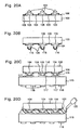
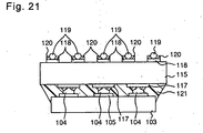
- Fig. 20A, Fig. 20B, Fig. 20C, Fig. 20D and Fig. 21 show the manufacturing method process by process.
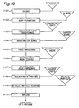
- Fig. 19 shows a process chart.
- step S101 of Fig. 19 dicing of a wafer is performed, and thereafter, a bump 104 is formed by the wire bonding method on each element electrode 105 of a semiconductor device 103 in step S102 as shown in Fig. 20A .
- the reference numeral 106 denotes a passivation film for protecting the active surface of the semiconductor device 103.
- a conductive adhesive 116. is formed on the bump 104 by a transfer method.
- an epoxy-based adhesive which include particles of Ag, Cu, or the like as a filler, is principally employed.
- step S104 as shown in Fig. 20C , the semiconductor device 103 is mounted so that the bumps 104 of the semiconductor device 103 are electrically connected to the electrodes 117 of a circuit board 115 formed of ceramic, glass epoxy, or the like, and the conductive adhesive 116 is thermally hardened in step S105.
- the standard hardening conditions of the conductive adhesive 116 are 140°C for 20 minutes.
- thermosetting is performed in step S107.
- the average conditions of the thermosetting are 140°C for four hours.
- step S108 as shown in Fig. 21 , a solder paste 120 is printed on electrodes 118 formed on the side that belongs to the circuit board 115 and are opposite from the mounting surface of the semiconductor device 103, and thereafter, metallic particles 119 of Au, Cu, Ag, or the like are mounted in step S109 and made to pass through a reflow furnace in step S110, obtaining a semiconductor device package as shown in Fig. 18 .
- step S101 to step S110 The semiconductor device package shown in Fig. 18 is thus completed through the processes of step S101 to step S110.
- the circuit board 115 has a thickness of about 0.5 mm, and a total thickness of the semiconductor package becomes about 1 mm including the thickness of the semiconductor device 103.
- This structure has had difficulties in being reduced in thickness and the issue that the package cannot be applied to a commodity, which is restricted to a thickness of not greater than 0.76 mm as in, for example, a noncontact IC card.
- the object of the present invention is to solve the aforementioned issues and provide a thin type semiconductor device package manufacturing method with high quality and high productivity, an electronic component module manufacturing method, a noncontact IC card manufacturing method, utilizing the semiconductor device package manufacturing method, a semiconductor device package manufactured by the semiconductor device package manufacturing method, a method for manufacturing a semiconductor device-mounted component such as a semiconductor device package and an electronic component module, a method for manufacturing a semiconductor device-mounted finished-product utilizing the semiconductor device-mounted component manufacturing method and a semiconductor device-mounted finished-product manufactured by the semiconductor device-mounted finished-product manufacturing method.
- JP 10270497 discloses a method for fixing semiconductor elements. In order to reduce the time, which is necessary for connecting a semiconductor element with a circuit board, and in order to obtain excellent electric characteristics and humidity resistance reliability, it is suggested to fix a semiconductor element via a thermoplastic insulating adhesive film, when bump electrodes of a semiconductor element are directly connected with a circuit board.
- US 4,625,102 discloses a method of manufacturing a memory card including the steps of taking an electronic module, which includes an insulating substrate and an integrated circuit and locally raising the temperature of the plastic material of the card to its softening point. The module is then applied with pressure, on one side of the card at its softened location to embed the module in the plastic material.
- a method and a device for mounting electronic components on a circuit board is disclosed.
- a bump is formed on an electrode on the IC chip, and the bump and an electrode of the circuit board are aligned with each other, while an insulating thermosetting resin free of conductive particles is provided between the electrode of the circuit board and the bump.
- the resin provided between the IC chip and the circuit board is hardened. Accordingly, the IC chip and the circuit board are joined with each other.
- Fig. 1A and Fig. 1B are partial sectional views showing the schematic constructions of semiconductor device packages according to the first illustrative example and the second illustrative example useful to explain the present invention.
- the semiconductor device package of the first embodiment is constructed of a semiconductor device 3 in which a bump 4 is formed on each element electrode 5 by the wire bonding method and a thermoplastic resin portion 7 that covers the periphery of the semiconductor device 3.
- the end surface 9 of each bump 4 is exposed on the surface of the thermoplastic resin portion 7, providing a structure for enabling electrical connection to the outside.
- the reference numeral 6 denotes a passivation film for protecting the active surface of the semiconductor device 3.
- end surfaces of the side portions of the semiconductor device 3 are structured so as to be covered with the thermoplastic resin portion 7 as indicated by the encircled number 1 (1) in Fig. 1A , it is acceptable to adopt a structure in which the end surfaces of the side portions of the semiconductor device 3 are exposed as indicated by the encircled number 2 (2) in Fig. 1B .
- Fig. 2 is a process chart showing the semiconductor device package manufacturing method of the first illustrative example.
- Fig. 3A, Fig. 3B, Fig. 3C, Fig. 3D and Fig. 3E are partial sectional views for explaining the semiconductor device package manufacturing method of the first embodiment of Fig. 2 .
- Fig. 4A and Fig. 4B are partial sectional views for explaining the semiconductor device package manufacturing method of the first embodiment of Fig. 2 , continued from Fig. 3E .
- Fig. 5A, Fig. 5B and Fig. 5C are partial sectional views for explaining the external appearance of the bumps' on the semiconductor device electrode of the first illustrative example.
- reference numeral 1 denotes a semiconductor wafer and 2 denotes a dicing saw.
- step S1 of Fig. 2 the semiconductor wafer 1 is diced to be divided into each piece of the semiconductor device 3.
- step S2 as shown in Fig. 3B , a bump 4 is formed on each element electrode 5 of the semiconductor device 3 divided into each individual piece by the wire bonding method using a metallic wire formed of Au, Cu, solder, or the like.
- thermoplastic resin sheet 7a formed of a thermoplastic resin of polyethylene terephthalate, vinyl chloride, polycarbonate, acrylonitrile butadiene styrene, or the like.
- the thickness of the thermoplastic resin sheet 7a is preferably basically not greater than a total thickness of the thickness of the semiconductor device 3 and the height of the bump 4. For example, when the thickness of the semiconductor device 3 is 0.18 mm and the height of the bump 4 is 0.04 mm, there is employed a thermoplastic resin sheet 7a of a thickness of 0.2 mm.
- step S4 by placing the thermoplastic resin sheet 7a on a hot pressing plate 8B arranged opposite to a hot pressing plate 8A, holding the thermoplastic resin sheet 7a on which the semiconductor device 3 is mounted between the hot pressing plates 8A and 8B, and pressurizing the hot pressing plate 8A against the hot pressing plate 8B relatively to each other, hot pressing is carried out to melt the thermoplastic resin sheet 7a, with which the surface of the semiconductor device 3 except for the upper surface is covered and the side surfaces of the bumps 4 of the semiconductor device 3 are covered, exposing only the end surfaces 9 of the bumps.
- the melted thermoplastic resin sheet 7a is cooled to constitute the thermoplastic resin portion 7.
- the hot pressing conditions when, for example, polyethylene terephthalate is employed for the thermoplastic resin sheet 7a, the conditions include a pressure of 30 kg/cm 2 (about 30 ⁇ 10 5 Pa), a temperature of 120°C, and a pressing time of one minute. It is to be noted that the temperature and the pressure are varied depending on the material of the thermoplastic resin sheet 7a.
- Fig. 3E is a sectional view showing a state after the hot pressing.
- step S5 the thermoplastic resin portion 7 is cut in specified positions A shown in Fig. 4A .
- a distance from the end surface of the side portion of the semiconductor device 3 to the cutting position A is not particularly specified.
- a semiconductor device package of the first illustrative example is completed in step S7 as shown in Fig. 4B .
- the bump 4 formed on the electrode 5 of the semiconductor device 3 may be a bump 4 of the shape shown in Fig. 5A (generally called the ton-off bump) or a bump 4A of the shape shown in Fig. 5B (generally called the two-step projection bump).
- the two-step projection bump 4A that has a small height variation dimension B is more desirable because the area C of the end surface 9 of the bump 4 exposed from the surface of the thermoplastic resin portion 7 after the hot pressing is more stabilized as shown in Fig. 5C .
- the semiconductor device package which has the total thickness of those of the semiconductor device 3 and the thermoplastic resin portion 7 as shown in step S7 of Fig. 2 , can be remarkably reduced in thickness, dissimilar to the semiconductor device package shown in the prior art example of Fig. 21 . Moreover, because of the absence of the conductive adhesive 16 and the encapsulant 21 shown in Fig. 21 and because of no time required for the hardening of the conductive adhesive and the encapsulant, the productivity can be remarkably improved.
- Fig. 6 is a process chart showing the semiconductor device package manufacturing method of the second illustrative example of the present invention.
- the semiconductor device package manufacturing method of the second illustrative example differs from the first illustrative example in that bumps 4 are formed in the state of the semiconductor wafer 1 in step S11 of Fig. 6 and thereafter dicing is performed in step S12 for the division into each individual piece of the semiconductor device 3.
- This second illustrative example is similar to the steps S3, S4 and S5 of the first illustrative example in the points of the mounting on the thermoplastic resin sheet 7a in step S13, the hot pressing performed in step S14, and the cutting of the thermoplastic resin portion 7 in step S15, respectively.
- the semiconductor device package which has the total thickness of those of the semiconductor device 3 and the thermoplastic resin portion 7, can be remarkably reduced in thickness, dissimilar to the semiconductor device package shown in the prior art example of Fig. 21 .
- the productivity can be remarkably improved.
- FIG. 7 is a process chart showing the semiconductor device package manufacturing method of the third illustrative example.
- Fig. 8A, Fig. 8B and Fig. 8C are explanatory views for explaining the semiconductor device package manufacturing method of the third illustrative example of Fig. 7 .
- Fig. 9A, Fig. 9B and Fig. 9C are partial sectional views for explaining the semiconductor device package manufacturing method of the third illustrative example of Fig. 7 , continued from Fig. 8C .
- a bump 4 is formed on each electrode element of a semiconductor wafer 1 by the wire bonding method.
- the reference numeral 61 denotes a capillary that is provided for a wire bonding device and holds a metallic wire formed of Au, Cu, solder, or the like, while the reference numeral 60 denotes a horn that belongs to the wire bonding device, holds the capillary 61 and applies a pressure and a supersonic wave.
- thermoplastic resin sheet 7b formed of a thermoplastic resin of polyethylene terephthalate, vinyl chloride, polycarbonate, acrylonitrile butadiene styrene, or the like is arranged oppositely to the semiconductor wafer 1 on which the bumps 4 are formed.
- the thickness of the thermoplastic resin sheet 7b is preferably basically not greater than the height of the bump 4. For example, when the height of the bump 4 is 0.04 mm, there is employed a thermoplastic resin sheet 7b of a thickness of 0.03 mm.
- step S23 as shown in Fig. 8C , by placing the semiconductor wafer 1 on a hot pressing plate 8D arranged opposite to a hot pressing plate 8C, holding the semiconductor wafer 1 and the thermoplastic resin sheet 7b arranged opposite to the semiconductor wafer 1 between the hot pressing plates 8C and 8D, and pressurizing the hot pressing plate 8C against the hot pressing plate 8D relatively to each other, the hot pressing is carried out to melt the thermoplastic resin sheet 7b, with which the upper surface of the semiconductor wafer 1 is covered and the side surfaces of the bumps 4 of the semiconductor wafer 1 are covered, exposing only the end surfaces 9 of the bumps. The melted thermoplastic resin sheet 7b is cooled to constitute the thermoplastic resin portion 7.
- the hot pressing conditions when, for example, polyethylene terephthalate is employed for the thermoplastic resin sheet 7b, the conditions include a pressure of 30 kg/cm 2 (about 30 ⁇ 10 5 Pa), a temperature of 120°C, and a pressing time of one minute. It is to be noted that the temperature and the pressure are varied depending on the material of the thermoplastic resin sheet 7b.
- Fig. 9A is a sectional view showing a state after the hot pressing.
- step 524 as shown in Fig. 9B , the semiconductor wafer 1 with the thermoplastic resin portion 7 formed through the hot pressing of the thermoplastic resin sheet 7b is diced by the dicing saw 2 and cut into each individual piece of the semiconductor device 3.
- Fig. 9C is a sectional view showing the semiconductor device package 3 obtained after the division, and the semiconductor device 3 shown in Fig. 1B come to have a structure of 2 in which the end surfaces of the side portions thereof are exposed.
- the semiconductor device package of the third illustrative example is completed.
- the semiconductor device package which has the total thickness of those of the semiconductor device 3 and the thermoplastic resin portion 7, can be remarkably reduced in thickness, dissimilar to the semiconductor device package shown in the prior art example of Fig. 12 .
- the productivity can be remarkably improved.
- Fig. 10A and Fig. 10B are partial sectional views for explaining the semiconductor device package of the first embodiment of the present invention.
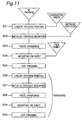
- Fig. 11 is a process chart showing the semiconductor device package manufacturing method of the first embodiment of Fig. 10A and Fig. 10B .
- the semiconductor device package of the first embodiment as shown in Fig. 10A and Fig. 10B , the semiconductor device package of the first illustrative example or/and the second illustrative example shown in Fig. 1A and Fig.
- thermoplastic resin portion 7 has a structure in which a circuit pattern is formed of a conductive paste 12 on a thermoplastic resin portion 7 on which the end surface 9 of each bump 4 is exposed, a metallic particle 11 is mounted on the conductive paste 12 is covered with a thermoplastic resin portion 7c, and the end surface of the metallic particle 11 is exposed on the surface of the thermoplastic resin portion 7c.
- a circuit pattern is formed of a conductive paste 12 on each electrode end surface side (i.e., the end surface side of each bump 4) of the semiconductor device package shown in Fig. 1A or Fig. 1B manufactured in accordance with the first illustrative example or the second illustrative example.
- the conductive paste 12 may be either the thermosetting type or the thermoplastic type.
- step S32 the metallic particles 11 are mounted in specified positions of the circuit pattern formed in the step S31, and the conductive paste 12 for forming the circuit pattern is thermally hardened in step S33.
- the metallic particle 11 is provided by Au, Cu, Ni, or the like capable of achieving electric conduction and is allowed to have a spherical or another shape in terms of shape. Its size is determined depending on the thickness of the thermoplastic resin sheet located on the covered side in step S34 and dimensioned so that the end surfaces of the metallic particles 11 are exposed from the thermoplastic resin sheet after the hot pressing in step S35 and able to achieve electric conduction to the outside. For example, when a thermoplastic resin film of a thickness of 100 ⁇ m is employed, a metallic particle 11 having a diameter of about 0.5 mm is employed.
- thermosetting conditions of the conductive paste 12 have the standard values of 140°C and about 10 minutes.
- step S34 the thermoplastic resin sheet is arranged oppositely to the surface on which the circuit pattern of the semiconductor device package is formed.
- step S35 by performing hot pressing and cutting the thermoplastic resin sheet as the occasion demands, the semiconductor device package shown in Fig. 10A is completed.
- the thermoplastic resin portion 7c is constructed of the thermoplastic resin sheet.
- step S35 By stopping the process flow after the step S35 without proceeding to step S36, the semiconductor device package shown in Fig. 10A is completed. Further, as the occasion demands, after step S35, by performing the five processes of a circuit pattern printing process of step S36 (process similar to step S31), a metallic particle mounting process of step S37 (process similar to step S32), a paste hardening process of step S38 (process similar to step S33), a mounting process onto a sheet of step S39 (process similar to step S34), and a hot pressing process of step S40 (process similar to step S35), a circuit pattern is formed of the conductive paste 12 on the end surface sides of the metallic particles 11 exposed from the thermoplastic resin portion 7c of the semiconductor package of Fig.
- thermoplastic resin portion 7d the multi-layered semiconductor package shown in Fig. 10B can be produced.
- a thermoplastic resin portion including the circuit pattern and the metallic particles 11 can further be formed in the number required on the thermoplastic resin portion 7d.
- the semiconductor device package which has the total thickness of those of the semiconductor device 3 and the thermoplastic resin portion, can be remarkably reduced in thickness, dissimilar to the semiconductor device package shown in the prior art example of Fig. 21 .
- the productivity can be remarkably improved.
- a multi-layered high-density semiconductor package can be supplied at low cost.
- Fig. 12 is a partial sectional view for explaining the semiconductor device package of the second embodiment of the present invention.
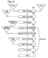
- Fig. 13 is a process chart showing the semiconductor device package manufacturing method of the second embodiment.
- the semiconductor device package described in connection with the third illustrative example has a structure in which a circuit pattern is formed of a conductive paste 12 on a thermoplastic resin portion 7 where the end surface 9 of each bump 4 is exposed, metallic particles 11 mounted on the circuit pattern are covered with a thermoplastic resin portion 7c, and the end surface of each metallic particles 11 are exposed on the surface of the thermoplastic resin portion 7c.
- Step S51 through step S53 of Fig. 13 are similar to the step S21 through step S23 of Fig. 7 of the third illustrative example, i.e., the processes of forming the bumps 4 on the semiconductor wafer 1, then making the thermoplastic resin sheet 7 oppose to the wafer, and performing the hot pressing.
- step S54 a circuit pattern is formed of the conductive paste 12 on the electrode end surface side, i.e., the bump end surface side of the semiconductor wafer 1 against which the thermoplastic resin sheet 7 is hot-pressed.
- the conductive paste 12 may be either the thermosetting type or the thermoplastic type.
- step S55 the metallic particles 11 are mounted in the specified positions of the circuit pattern, and the conductive paste 12 that forms the circuit pattern is thermally hardened in step S56.
- the metallic particle 11 is provided by Au, Cu, Ni, or the like capable of achieving electric conduction and is allowed to have a spherical or another shape. Its size is determined depending on the thickness of a new thermoplastic resin sheet other than the thermoplastic resin sheet 7 located on the covered side and dimensioned so that the end surfaces of the metallic particles 11 are exposed from the thermoplastic resin sheet after the hot pressing and able to achieve electric conduction to the outside. For example, when a thermoplastic resin sheet of a thickness of 100 ⁇ m is employed, a metallic particle 11 having a diameter of about 0.5 mm is employed.
- thermosetting conditions of the conductive paste 12 have the standard values of 140°C and about 10 minutes.
- step S57 by using hot pressing plates similar to the hot pressing plates 8C and 8D shown in Fig. 8C , placing the semiconductor wafer 1 on the other hot pressing plate opposite to one hot pressing plate, arranging the thermoplastic resin sheet oppositely to the surface which belongs to the semiconductor wafer 1 and on which the circuit pattern is formed, holding the sheet between the pair of hot pressing plates, and pressurizing one hot pressing plate against the other hot pressing plate relatively to each other, the hot pressing is carried out in step S58 to melt the thermoplastic resin sheet, with which the upper surface of the' semiconductor wafer 1- is covered and the side surface of each metallic particle 11 of the semiconductor wafer 1 is covered, exposing only the end surfaces of the particles. The melted thermoplastic resin sheet is cooled to constitute a thermoplastic resin portion 7c.
- thermoplastic resin portion 7c that includes the circuit pattern and the metallic particles 11 is formed on the thermoplastic resin portion 7.
- a thermoplastic resin portion 7d that includes the circuit pattern and the metallic particles can be formed on the thermoplastic resin portion 7c as shown in Fig. 12 , allowing the multi-layer formation to be easily performed.
- step S54 through step S58 in required times, the required number of thermoplastic resin portions that include the circuit patterns and the metallic particles can be formed on the previously formed thermoplastic resin portion.
- step S59 by dicing the semiconductor wafer 1 against which the thermoplastic resin sheet is thermally pressed, the semiconductor device package shown in Fig. 12 is completed.
- the semiconductor device package which has the total thickness of those of the semiconductor device and the thermoplastic resin portion, can be remarkably reduced in thickness, dissimilar to the semiconductor device package shown in the prior art example of Fig. 21 .
- the productivity can be remarkably improved.
- the multi-layered high-density semiconductor package can be supplied at low cost.
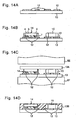
- Fig. 14A, Fig. 14B, Fig. 14C and Fig. 14D are partial sectional views for explaining the electronic component module manufacturing method of the fourth illustrative example.
- Fig. 15 is a process chart showing the electronic component module manufacturing method of the fourth illustrative example.
- the electronic component module manufacturing method of the fourth illustrative example is related to electronic component modules that employ the semiconductor device packages described in connection with the first illustrative example through the second embodiment.
- the reference numeral 13 denotes a film substrate formed of a thermoplastic resin of polyethylene terephthalate, vinyl chloride, polycarbonate, acrylonitrile butadiene styrene, or the like.
- a circuit pattern is formed of a thermosetting or thermoplastic type conductive paste 12 on the film substrate 13.
- step S62 a semiconductor package 14 and an electronic component 15 such as a passive component of a resistor, capacitor, or the like are mounted in specified positions of the circuit pattern, and thereafter, the conductive paste 12 is thermally hardened.
- thermoplastic resin sheet 13A is arranged as a cover sheet on the semiconductor package 14 and the electronic component 15 oppositely to the side on which the circuit board of the film substrate 13 is formed and held between the hot pressing plates 8E and 8F.
- the thickness of the thermoplastic resin sheet 13A is preferably not smaller than either thicker one of the semiconductor device package 14 or the electronic component 15.
- step S64 hot pressing is carried out to melt the thermoplastic resin sheet 13A by pressurizing the hot pressing plate 8E against the hot pressing plate 8F relatively to each other, so that at least the upper surfaces and the side surfaces of the semiconductor package 14 and the electronic component 15 are covered with the sheet.
- the melted thermoplastic resin sheet 13A is cooled to constitute a thermoplastic resin portion 13B.
- the electronic component module shown in Fig. 14D is completed.
- the electronic component module which has a thickness almost equal to the total thickness of those of the semiconductor device package 14 and the electronic component 15 and the thermoplastic resin portion, can be reduced in thickness, which cannot be achieved by electronic component module of the prior art example.
- the thermoplastic resin portion secures the reliability of the semiconductor device and the electronic component, there is required neither encapsulant nor a time for the hardening of the encapsulant, dissimilar to the conventional case, and this allows the productivity to be remarkably improved.
- the low material cost enables the supply of an inexpensive electronic component module.
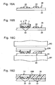
- Fig. 16A, Fig. 16B, Fig. 16C and Fig. 16D are partial sectional views for explaining the noncontact IC card manufacturing method of the fifth illustrative example of the present invention.
- Fig. 17 is a process chart showing the noncontact IC card manufacturing method of the seventh embodiment.
- the fifth illustrative example is an example of application to a noncontact IC card constructed of a semiconductor device that has a noncontact IC card-use IC chip and an antenna coil that executes transmission and reception to and from the outside.
- the reference numeral 23 denotes a film substrate as one example of a thermoplastic resin base material formed of a thermoplastic resin of polyethylene terephthalate, vinyl chloride, polycarbonate, acrylonitrile butadiene styrene, or the like.
- a circuit pattern is formed of a thermosetting or thermoplastic type conductive paste 22, and a coil 26 is formed for executing data transmission and reception to and from the outside.
- step S72 as shown in Fig. 16B , a semiconductor package 14 that has an IC chip for use in a noncontact IC card is mounted in a specified position of the circuit pattern, and thereafter, the conductive paste 22 is thermally hardened in step S73.
- step S74 as shown in Fig. 16C , the film substrate 23 is placed on a hot pressing plate 8H arranged opposite to a hot pressing plate 8G, and a thermoplastic resin sheet 23A is arranged as a cover sheet on the semiconductor package 14 oppositely to the side of the film substrate 23 on which the circuit board is formed, and the film substrate 23 and the sheet 23A is held between the hot pressing plates 8G and 8H.
- the thickness of the thermoplastic resin sheet 23A is preferably not smaller than the thickness of the semiconductor device package 14 and is able to be arbitrarily selected according to the required card thickness.
- the thickness of the film substrate 23 is set to 0.2 mm, and the thickness of the thermoplastic resin sheets 23A is set to 0.5 mm.
- step S75 by pressurizing the hot pressing plate 8G against the hot pressing plate 8H relatively to each other, hot pressing is carried out to melt the thermoplastic resin sheet 23A, then completely covering the semiconductor device package 14 and the coil 26 and the like located on the side where the circuit board of the film substrate 23 is formed.
- the melted thermoplastic resin sheet 23A is cooled to constitute a thermoplastic resin portion 23B.
- step S76 by cutting the sheet into a card size by punching or the like, the noncontact IC card of the sectional structure shown in Fig. 16D is completed.
- the casing of the noncontact IC card concurrently serves as the substrate, and therefore, a thin IC card, which has not conventionally existed, can be formed.
- the semiconductor device package can be directly mounted onto the circuit pattern paste formed of the conductive paste prior to the drying of the paste, the productivity is remarkably improved.
- the process has been complicated and the productivity has been low since the process has included the steps of drying the paste, thereafter mounting the semiconductor device via an anisotropic conductive resin sheet or anisotropic conductive particles, and then performing thermocompression bonding.
- a thin type semiconductor device package which has conventionally not existed, can be provided at low cost with high productivity.
- the electronic component module and the noncontact IC card can be provided at low cost with high productivity.
- the third embodiment of the present invention is related to a semiconductor component-mounted component manufacturing method for manufacturing a semiconductor component-mounted component by mounting on as substrate an electronic component such as an IC chip, used for a case of electrically connecting the IC chip to connection pads provided for a circuit pattern constructed of a conductive paste as in the case of manufacturing, for example, a noncontact IC card, a manufacturing method for manufacturing a semiconductor component-mounted finished-product that has a semiconductor component-mounted component manufactured by the above manufacturing method.
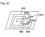
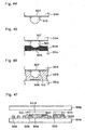
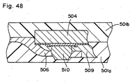
- Fig. 41 through Fig. 48 show a conventional noncontact IC card and a manufacturing method therefor.
- a coil pattern 502 is formed of a conductive paste on a first base material 501a, and a connection pad 506 provided at the outer peripheral terminal 503a of this coil pattern 502 and a connection pad 506 provided at the inner peripheral terminal 503b of the coil pattern 2 are electrically connected to the electrode portions of the IC chip 504.
- the manufacturing process thereof has the step of printing a circuit pattern including the coil pattern 502 with a conductive paste on the surface of the first base material 501a.
- a conductive paste As the above-mentioned conductive paste, silver paste is appropriately used.
- the printing of the conductive paste is performed by screen printing, offset printing, gravure printing, or the like.
- a conductive paste is printed on the first base material 501a via a mask of 165 meshes/inch and an emulsion thickness of 10 ⁇ m, thus forming a circuit pattern of a conductor thickness of about 30 ⁇ m.
- thermoplastic resin which has a thickness of about 0.1 to 0.5 mm and is made of polyethylene terephthalate, vinyl chloride, polycarbonate, acrylonitrile butadiene styrene, or the like, is used for the first base material 501a and the second base materials 502b described later.
- step S302 the conductive paste is hardened by heating the circuit pattern made of the aforementioned conductive paste formed on the first base material 501a by the printing method at a temperature of 120°C for ten minutes.
- an anisotropic conductive sheet 509 is stuck to the connection pads 506 provided at the outer peripheral terminal 503a and the inner peripheral terminal 503b of the circuit pattern.
- the anisotropic conductive sheet is a resin sheet that contains metallic particles and operates to electrically connect the metallic particles with the connection pads 506 by being heated and pressurized.
- step 304 the anisotropic conductive sheet 509 is heated at a temperature of 100°C for five seconds so as to be temporarily pressure-bonded to the connection pads 506.
- step S305 a semiconductor device 504 and components of a capacitor and the like are mounted on the temporarily pressure-bonded anisotropic conductive sheet 509.
- bumps 510 are formed on electrode pads 507 on the semiconductor device 504 as shown in Fig. 44 , and the bumps 510 and the connection pads 506 are electrically connected together via the anisotropic conductive sheet 509 as shown in Fig. 45 .
- the bump 510 is formed on the electrode pad 507 of the semiconductor device 504 by the wire bonding method or the plating method; or concretely by the plating method which uses solder, gold, silver, copper, or the like.
- step 306 the anisotropic conductive sheet is hardened by being heated at a temperature of 200°C for 30 seconds as shown in Fig. 46 , regularly pressure-bonding the semiconductor device 504.
- the mounting of the semiconductor device is completed by this step 306.
- step S307 by sticking the second base material 501b to the first base material 501a to perform a laminating process, an IC card in which the connection pads 506 and the bumps 510 are electrically connected together via the anisotropic conductive paste 509 is obtained as shown in Fig. 47 .
- the reference numeral 505 denotes a capacitor connected parallel to the coil pattern 502.
- thermoplastic resin such as polyethylene terephthalate and vinyl chloride is used for the first base material 501a and the second base material 501b.
- the conventional manufacturing process which has a high temperature of not lower than 200°C in regularly pressure-bonding the semiconductor device 504 via the anisotropic conductive sheet 509 in step S306, has the issue that the first base material 501a and the second base material 501b inferior in terms of heat resistance easily deteriorate.
- anisotropic conductive particles used in place of the anisotropic conductive sheet 509.
- the semiconductor device 504 is heated and pressurized when performing the laminating process in the step 307. Therefore, as shown in Fig. 48 , the semiconductor device 504 sinks in the first base material 501a, and the circuit pattern 506 provided by the conductive paste is disadvantageously deformed in a curve. As a result, there is high possibility of circuit pattern disconnection, and a deficiency of operation trouble occurs.
- the third embodiment of the present invention is intended to solve the above-mentioned issues and has the object of providing a manufacturing method of a semiconductor component-mounted component and a manufacturing method of a semiconductor component-mounted finished-product, which have high-quality, high-productivity, and low cost.
- the manufacturing method of the semiconductor component-mounted finished-product is the manufacturing method for manufacturing a semiconductor component-mounted finished-product that has a semiconductor component-mounted component manufactured by the manufacturing method of the semiconductor component-mounted component, while the semiconductor component-mounted finished-product has the semiconductor component-mounted component manufactured by the manufacturing method of the semiconductor component-mounted component and is manufactured by the manufacturing method of the semiconductor component-mounted finished-product. It is to be noted that the same components are denoted by the same reference numerals in each figure.
- a first thermoplastic resin base material 422 is taken as one example that fulfills the function of the aforementioned "base material” in the present eighth embodiment
- a bump 413 is taken as one example that fulfills the function of a "circuit connection portion” in the present third embodiment.
- a projecting portion 418, a rugged portion 1131, and an exposed surface 1132 are taken as one example that fulfills the function of a "contact area increasing portion” in the present eighth embodiment.
- Extension portion-forming members 450, 455 and 457, a heating device 453, and an extension portion-forming member-use pressurizing device 454 are taken as one example that fulfills the function of a "contact area increasing devices" in the present third embodiment.
- a noncontact IC card is taken as one example that fulfills the function of the "semiconductor component-mounted finished-product" in the present third embodiment, the present invention is, of course, not limited to this.
- Fig. 22 shows a noncontact IC card 401 that serves as one example of the semiconductor component-mounted finished-product provided with the semiconductor component-mounted component manufactured by the manufacturing method of the semiconductor component-mounted component of the present third embodiment.
- a semiconductor device 414 is preparatorily embedded in the first thermoplastic resin base material 422, forming the projecting portions 418 on member forming surfaces 415 that belong to the bumps 413 and are exposed to a pattern forming surface 423 of the first thermoplastic resin base material 422. Then, a circuit pattern 416 formed of a conductive paste and the projecting portions 418 directly obtain conduction without interposition of an anisotropic conductive paste or the like, dissimilar to the prior art example.
- the reference numerals 424 and 425 denote a second thermoplastic resin sheet base material and a third thermoplastic resin sheet base material for performing laminating process to protect a semiconductor component-mounted component 421 that has the semiconductor device 414 and the circuit pattern 416 and are used for the laminating process corresponding to the encapsulating operation of the semiconductor component-mounted component 421 by the encapsulating devices 426 and 427.
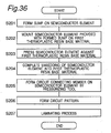
- the manufacturing procedure of the noncontact IC card 401 will be described below with reference to Fig. 23 through Fig. 29 and Fig. 36 .
- the reference numeral 417 denotes the electrode of the semiconductor devices 414 corresponding to a semiconductor component
- the reference numeral 412 denotes a passivation film for protecting the active surface of the semiconductor device 414.
- step S202 shown in Fig. 24 and Fig. 36 one or a plurality of semiconductor devices 414 on which the bumps 413 are formed are mounted on a sheet-shaped first thermoplastic resin base material 422 formed of a thermoplastic resin of polyethylene terephthalate, vinyl chloride, polycarbonate, acrylonitrile butadiene styrene, or the like, which has an electrical insulating property.
- the thickness of the first thermoplastic resin base material 422 is preferably basically greater than the thickness of the semiconductor device 414 and not greater than the total thickness of the thickness of the semiconductor device 414 and the height of the bump 413 for the reason that at least the member forming surfaces 415 of the bumps 413 are required to be exposed from the first thermoplastic resin base material 422, as described later.
- the first thermoplastic resin base material 422 preferably has a thickness of 0.2 mm.
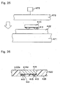
- the first thermoplastic resin base material 422 on which the semiconductor device 414 provided with the bumps 413 is mounted is held between hot pressing plates 471 and 472, and the semiconductor device 414 provided with the bumps 413 and the first thermoplastic resin base material 422 are pressurized relatively to each other by a semiconductor part pressurizing device 473 with heat applied to them, inserting the semiconductor device 414 into the first thermoplastic resin base material 422.
- the hot pressing conditions include a pressure of 30 ⁇ 10 5 Pa, a temperature of 120°C, and a pressing time of one minute. The temperature and the pressure are varied according to the material of the first thermoplastic resin base material 422.
- Fig. 26 corresponding to step 204 is a sectional view showing the state of the semiconductor device 414 and the first thermoplastic resin base material 422 obtained after the pressing.
- the semiconductor device 414 and the bumps 413 are embedded in the first thermoplastic resin base material in a state in which the end surfaces of the bumps 413, i.e., the member forming surfaces 415 that are surfaces on which the bumps 413 are brought in contact with the hot pressing plate 471 is exposed to the pattern forming surface 423 of the first thermoplastic resin base material 422 by the aforementioned pressing.
- the present eighth embodiment for decreasing its thickness, it is constructed so that a back surface 414a opposite from the active surface of the semiconductor device 414 and a back surface 422a of the first thermoplastic resin base material 422 opposite from the pattern forming surface are flush with each other as shown in the figure.
- the present invention is not limited to this. That is, depending on the semiconductor component-mounted component to be manufactured, it is acceptable to make the back surface 414a of the semiconductor device 414 project from, for example, the back surface 422a of the first thermoplastic resin base material 422 by adjusting the thickness of the first thermoplastic resin base material 422, the pressurization force of the hot pressing plates 471 and 472, or the like.
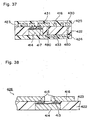
- the member forming surface 415 is one example for fulfilling the function of the electric connection surface. Moreover, in the present eighth embodiment, only the member forming surfaces 415 are exposed from the pattern forming surface 423 of the first thermoplastic resin base material 422. However, by devising the shape of, for example, the pressing plate 471, it is acceptable to expose not only the member forming surfaces 415 but also parts or the wholes of the bumps 413 from the pattern forming surface 423. If this construction is adopted, the electrical connection surface corresponds to the external surface of the portion exposed from the pattern forming surface 423. It is to be noted that Fig. 38 shows a case in which the member forming surfaces 415 of the bumps 413 and their peripheral portions are exposed from the pattern forming surface 423.
- step 205 of Fig. 27 and Fig. 36 by pressurizing the member forming surfaces 415 of the bumps 413 exposed on the pattern forming surface 423 of the first thermoplastic resin base material 422 by an extension portion-forming member 450, the projecting portions 418 are formed integrally with the bumps 413 from the bumps 413 on the member forming surfaces 415.
- a cylindrical structure that internally has a hollow portion 451 is employed as the extension portion-forming member 450.
- a heating device 453 connected to the extension portion-forming member 450 and pressurizing the tip 452 of the extension portion-forming members 450 against the member forming surfaces 415 with a load of 100g per bump by means of the extension portion-forming member-use pressurizing device 454, the member forming surfaces 415 are deformed, and parts of the bumps 413 enter a hollow portion 450a. Therefore, after the pressurization, rectangularly projecting portions 418 projecting from the member forming surfaces 415 are formed integrally with the bumps 413 on the member forming surfaces 415.
- the projecting portions 418 By forming the projecting portions 418 as described above, a contact area with the circuit pattern of a conductive paste described later is increased further than when the circuit pattern is formed on the member forming surfaces 415, and therefore, the reliability' of bonding is increased. Moreover, since the projecting portions 418 are formed by the extension portion-forming embers 450, further cost reduction can be achieved than when bumps are further formed on, for example, the bumps 413.
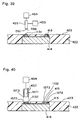
- the extension portion-forming member 450 is not limited in shape to the above-mentioned one and is also able to be provided by one whose tip 456 is preferably sharpened or preferably provided with a plurality of rugged portions 1561 as, for example, a rod-shaped extension portion-forming member 455 as shown in Fig. 39 .
- the rugged portions 1561 of the extension portion-forming member 455 as described above against the member forming surfaces 415 of the bumps 413, the rugged portions 1131 can be formed on the member forming surfaces 415, and the contact area of the circuit pattern of the conductive paste described later with the bumps 413 can be increased, allowing the reliability of bonding to be increased.
- an extension portion-forming member 457 as shown in Fig. 40 can also be employed.
- the extension portion-forming member 457 has a hollow portion 1571 that has a capacity for accommodating therein the bumps 413 and a tip portion 1573 that forms contact area increasing grooves 1572 for increasing the contact area of the circuit pattern of the conductive paste described later with the bump 413, around the bumps 413 when the tip portion of the extension portion-forming member' 457 is pressurized against the pattern forming surface 423 of the first thermoplastic resin base material 422.
- the contact area increasing grooves 1572 are formed around the bumps 413, and an exposed surface 1132 exposed from the first thermoplastic resin base material 422 is formed by the contact area increasing groove 1572. Therefore, the surface areas of the bumps 413 exposed from the pattern forming surface 423 can be increased, and the contact area of the circuit pattern of the conductive paste described later with the bumps 413 can be increased, allowing the reliability of bonding to be increased.
- the extension portion-forming member which forms the contact area increasing portion for increasing the contact area of the circuit pattern of the conductive paste described later with the bumps 413 can be used for the bumps 413.
- the projecting portion 418, the rugged portion 1131 formed on the member forming surface 415 by the rugged portion 1561, and the exposed surface 1132 exposed by the contact area increasing groove 1572 correspondingly serve as the contact area increasing portion.
- the rugged portion 1131 is formed on the bump, it is acceptable to form a rugged portion on the bump by a hot pressing plate provided with a rugged surface by utilizing the time of embedding of the semiconductor device 414 in the hot pressing plate 471 in step 203.
- the circuit pattern 416 electrically connected to the semiconductor device 414 is formed on the pattern forming surface 423 of the first thermoplastic resin base material 422 so as to make contact with the projecting portion 418 using a conductive paste of Ag, Cu, or the like or preferably so as to embed the projecting portion 418 as shown in the figure.
- the circuit pattern 416 to be electrically connected to the semiconductor device 414 is formed on the pattern forming surface 423 of the first thermoplastic resin base material 422 so as to make contact with the rugged portion 1131 and the exposed surface 1132 or preferably so as to embed them.
- the formation of the circuit pattern 416 of the conductive paste is generally performed by the screen printing, offset printing, gravure printing, or the like.
- a conductive paste is printed via a mask of 165 meshes/inch and an emulsion thickness of 10 ⁇ m, thus forming a circuit pattern 416 of a conductor thickness of about 30 ⁇ m.
- the circuit pattern 416 formed in the present eighth embodiment has the shape of an antenna coil for executing transmission and reception of information to and from the semiconductor device 414 in a wireless manner.
- the circuit pattern 416 is, of course, not limited to the aforementioned antenna coil shape and can be formed into a form corresponding to the functions of the semiconductor component-mounted component as a manufactured product.
- the semiconductor device 414 is thus mounted on the circuit pattern 416. Moreover, the constituent part in the mounted state shown in Fig. 28 is served as a semiconductor component-mounted component 421.
- step S207 of Fig. 29 and Fig. 36 the semiconductor component-mounted component 421 is sandwiched in the direction of thickness thereof between the second thermoplastic resin sheet base material 424 and the third thermoplastic resin sheet base material 425, which have a sheet-like shape and electrical insulating properties and are made of polyethylene terephthalate, vinyl chloride, polycarbonate, acrylonitrile butadiene styrene, or the like and then laminated by encapsulating devices 426 and 427, thus performing the encapsulation of the semiconductor component 421.
- the laminating process conditions include a pressure of 30 ⁇ 10 5 Pa, a temperature of 120°C, a pressing time of one minute, and a pressure retention time of one minute.
- the semiconductor component-mounted component that serves as a module on which the semiconductor device 414 is mounted as shown in Fig. 22 , and the noncontact IC card 401 corresponding to one example that fulfills the functions as a semiconductor component-mounted finished-product having the semiconductor component-mounted component as in the case of the present eighth embodiment is completed.
- the semiconductor device 414 is embedded in the first thermoplastic resin base material 422, and thereafter, they are formed into a card. Therefore, the sinking of the semiconductor device 504 into the base material 501a after the formation of a card, as in the prior art example shown in Fig. 48 , does not occur.
- circuit pattern 416 is not disconnected, and this enables the manufacturing of high-quality semiconductor component-mounted component and semiconductor component-mounted finished-product.
- a semiconductor component-mounted component 428 in which the circuit pattern 416 is formed on the pattern forming surface 423 in step 206 and thereafter, as shown in Fig. 30 , an electronic component 429 that serves as a passive component of a capacitor, a resistor, or the like is mounted in a specified position of the circuit pattern. Then, as shown in Fig. 31 , it is also possible to manufacture the noncontact IC card 402 as shown in Fig. 31 by sandwiching the semiconductor component-mounted component 428 in the direction of thickness thereof between the second thermoplastic resin base material 424 and the third thermoplastic resin base material 425 and then performing the laminating process.
- Fig. 32 shows a plan view showing the whole of the semiconductor component-mounted component 421 shown in Fig. 28 .
- Fig. 33 shows a sectional view taken along the line I-I shown in Fig. 32 .
- Fig. 34 shows a sectional view taken along the line I-I of the noncontact type IC card 401 obtained through the laminating process of the whole of the semiconductor component-mounted component 421 with the second thermoplastic resin sheet base material 424 and the third thermoplastic resin sheet base material 425.
- an insulating film 432 is provided for the circuit pattern 416 in order to jumper-connect an outer peripheral terminal 430 of the circuit pattern 416 with the corresponding portion 431 of the electrode 417 of the semiconductor device 414, and thereafter, the outer peripheral terminal 430 and the electrode corresponding portion 431 are electrically connected with each other by the printing of a conductive paste, a conductive foil 433, or the like. With this arrangement, a jumper as shown in the figure is completed. It is to be noted that the formation of the insulating film 432 is performed by the bonding of a polyester-based insulating foil or the printing of an insulating coating.
- the jumper connection of the outer peripheral terminal 430 of the circuit pattern 416 with the corresponding portion 431 of the electrode 417 of the semiconductor device 414 is not limited to the aforementioned method and is also able to be achieved by forming a circuit pattern 433 on the opposite side of the surface on which the circuit pattern 416 is formed by printing a conductive paste via a through hall 480 preparatorily provided in the first thermoplastic resin base material 422 as shown in, for example, Fig. 37 .
- the formation of the circuit pattern 433 may be performed before the embedding of the semiconductor device 414 in the first thermoplastic resin base material 422 or after the formation of the circuit pattern 416.
- the through hall 480 can be filled with the conductive paste concurrently with the printing of the circuit pattern 416 or the printing of the circuit pattern 433.
- the present invention is not limited to the construction. It is enabled to form the first thermoplastic resin base material 422 into a double-sided substrate and form the same into a form corresponding to the functions of the semiconductor component-mounted component that serves as a manufactured product.
- the semiconductor component-mounted component 421 or the semiconductor component-mounted component 428 are sandwiched between the two thermoplastic resin sheet base materials 424 and 425 when manufacturing the noncontact IC card as one example that fulfills the functions of a semiconductor component-mounted finished-product
- the present invention is not limited to the construction.
- the first thermoplastic resin base material 422 when the first thermoplastic resin base material 422 is placed on a plate and encapsulated, it is proper to employ only the third thermoplastic resin base material only 425, and it is proper to appropriately devise the use of the two thermoplastic resin base materials 424 and 425 according to the type and functions of the semiconductor component-mounted component to be manufactured.
- the present invention is not limited to this. That is, it is acceptable to expose, for example, the member forming surfaces 415 as projecting portions 418 by the extension portion-forming member 450 in the step 206 for the achievement of electrical connection to the circuit pattern 416 without exposing the member forming surfaces 415 on the pattern forming surface 423.
- the mounting is completed by forming the contact area increasing portion by the contact area increasing device on the circuit connection portion of the inserted semiconductor component after the insertion of the semiconductor component into the base material by the semiconductor component pressurizing device, and then forming the circuit pattern on the circuit connection portion that has the contact area increasing portion. Therefore, because neither the anisotropic conductive sheet nor the anisotropic conductive particles is used during mounting, remarkable improvement of the productivity and cost reduction can be achieved in comparison with the conventional case. Moreover, since the circuit pattern is formed on the semiconductor component inserted in the base material, the sinking of the semiconductor component, which has occurred in the conventional case, can be prevented. As a result, the high-quality semiconductor component-mounted component and semiconductor component-mounted finished-product free of the disconnection of the circuit pattern can stably be produced.
Landscapes
- Engineering & Computer Science (AREA)
- Computer Hardware Design (AREA)
- Microelectronics & Electronic Packaging (AREA)
- Physics & Mathematics (AREA)
- General Physics & Mathematics (AREA)
- Theoretical Computer Science (AREA)
- Encapsulation Of And Coatings For Semiconductor Or Solid State Devices (AREA)
- Wire Bonding (AREA)
Claims (11)
- Verfahren zur Herstellung einer verpackten Halbleitervorrichtung, mit den Schritten:Ausbilden von Erhebungen (4, 4a) auf Elementelektroden (5) eines Halbleiterwafers (1) mittels eines Drahtbond-Verfahrens,Positionieren eines thermoplastischen Harzbogens (7a) auf dem Halbleiterwafer (1),Ausbilden eines thermoplastischen Harzabschnitts (7) zum Bedecken eines Abschnitts der Halbleitervorrichtung (3) in einer Weise, dass die Endflächen (9) der Erhebungen (4) durch Schmelzen des thermoplastischen Harzbogens freigelegt sind, der eine Dicke aufweist, die nicht größer als die Höhe der Erhebungen (4) ist, indem der Halbleiterwafer (1) und der thermoplastische Harzbogen (7a) heißgepresst werden,Schneiden des Halbleiterwafers und des thermoplastischen Harzabschnitts, die dem Heißpressen unterzogen wurden,dadurch gekennzeichnet, dass vor dem Schneiden des Halbleiterwafers und des thermoplastischen Harzabschnitts die folgenden weiteren Schritte ausgeführt werden:Drucken eines Schaltungsmusters mit einer leitfähigen Paste (12) auf einer Elektrodenoberflächenseite des Halbleiterwafers,Härten der leitfähigen Paste, wobei ein metallisches Partikel (11) an einer bestimmten Position des Schaltungsmusters angeordnet ist,Ausbilden eines thermoplastischen Harzabschnitts (7c) zum Bedecken eines Abschnitts der Halbleitervorrichtung mit Ausnahme einer Endfläche des metallischen Partikels durch positionelles Ausrichten des Halbleiterwafers, der nach dem Härten der leitfähigen Paste erhalten wurde, mit dem thermoplastischen Harzbogen und Schmelzen des thermoplastischen Harzbogens mittels Heißpressens.
- Verfahren nach Anspruch 1, ferner mit:Erhalten einer Multischichtstruktur durch Wiederholen des Vorgangs des Ausbildens eines thermoplastischen Harzabschnitts (7c) zum Bedecken eines Abschnitts der Halbleitervorrichtung mit Ausnahme einer Endfläche des metallischen Partikels durch positionelles Ausrichten des Halbleiterwafers, der nach dem Härten der leitfähigen Paste erhalten wurde, mit dem thermoplastischen Harzbogen und des Schmelzens des thermoplastischen Harzbogens mittels Heißpressens und des nachfolgenden Schneidens des Halbleiterwafers, der das metallische Partikel aufweist und dem Heißpressen unterzogen wurde, in einer vorbestimmten Anzahl.
- Verfahren nach Anspruch 1 oder 2, ferner mit:Drucken eines Schaltungsmusters mit einer leitfähigen Paste (12) auf einen ersten thermoplastischen Harzbogen (13),Anbringen einer Halbleitervorrichtungspackung und eines elektronischen Bauteils (15) an bestimmten Positionen des Schaltungsmusters des ersten thermoplastischen Harzbogens, undAusbilden eines thermoplastischen Harzabschnitts (13B) zum Bedecken der Halbleiterpackung und des elektronischen Bauteils durch positionelles Ausrichten eines zweiten thermoplastischen Harzbogens (13A) mit dem ersten thermoplastischen Harzbogen, auf dem die Halbleitervorrichtungspackung und das elektronische Bauteil angebracht sind, und Schmelzen des zweiten thermoplastischen Harzbogens mittels Heißpressens.
- Verfahren zur Herstellung eines elektronischen Bauteilmoduls nach Anspruch 3, wobei, wenn der thermoplastische Harzabschnitt (7) gebildet wird, eine Oberfläche der Halbleitervorrichtung, auf der die Erhebung gebildet ist, mit Ausnahme der Endfläche (9) der Erhebung der Halbleitervorrichtung durch Schmelzen des thermoplastischen Harzbogens.
- Verfahren nach einem der Ansprüche 1 oder 2, ferner mit:Drucken eines Schaltungsmusters, das dazu in der Lage ist, elektrisch mit einem IC-Elektrodenabschnitt des IC-Chips oder einem Schaltungsmusters verbunden zu werden, das elektrisch mit dem IC-Elektrodenabschnitt zu verbinden ist, einschließlich eines Spulenmusters, das die Antennenspule bildet, auf einem thermoplastischen Harzbasismaterial (23) mit einer leitfähigen Paste (22),Anordnen einer Halbleitervorrichtungspackung auf dem Schaltungsmuster in einer Weise, dass der IC-Elektrodenabschnitt des IC-Chips der Halbleitervorrichtungspackung, die den IC-Chip aufweist und die durch das Verfahren zur Herstellung einer verpackten Halbleitervorrichtung nach einem der Ansprüche 1 oder 2 hergestellt ist, mit dem Schaltungsmuster verbunden ist,Härten der leitfähigen Paste,Ausbilden eines thermoplastischen Harzabschnitts (23B) zum Bedecken der Halbleitervorrichtungspackung durch positionelles Ausrichten eines thermoplastischen Harzbogens (23A) auf einer Halbleitervorrichtungspackungsanordnungsoberflächenseite des thermoplastischen Harzbasismaterials, das nach Härten der leitfähigen Paste erhalten wurde, und Schmelzen des thermoplastischen Harzbogens mittels Heißpressens, undSchneiden des thermoplastischen Harzabschnitts nach dem Heißpressen, wodurch die Karte gebildet wird.
- Verfahren nach Anspruch 1, ferner mit:Einfügen der Halbleitervorrichtung in das Basismaterial, wobei die Erhebung des Halbleitermaterials in einen freigelegten Zustand in der Nähe der Musterbildungsoberfläche gebracht wird, undAusbilden eines Kontaktbereichsvergrößerungsabschnitts (418, 1131, 1132) zum Vergrößern eines Kontaktbereichs des Schaltungsmusters mit der Erhebung auf der Erhebung, die auf der Schaltungsbildungsoberfläche freigelegt ist.
- Verfahren nach Anspruch 6, wobei
der Kontaktbereichsvergrößerungsabschnitt von einem Ausdehnungsabschnittsbildungselement (450, 455. 457) gebildet wird, das in Kontakt mit der Erhebung oder der Musterbildungsoberfläche gebracht wird, angeordnet in einer Nähe der Erhebung, wenn der Kontaktbereich vergrößert wird, und
das Ausdehnungsabschnittsbildungselement gegen die Erhebung oder gegen die Musterbildungsoberfläche gedrückt wird, die in der Nähe der Erhebung angeordnet ist. - Verfahren nach Anspruch 7, wobei, wenn das Ausdehnungsabschnittsbildungselement eine zylindrische Form aufweist, ein hervorstehender Bereich (418) als der Kontaktbereichsvergrößerungsabschnitt auf der gebildeten Erhebung durch einen Druckvorgang erzeugt wird, zum Durchführen eines Drückens mit dem Ausdehnungsabschnittsbildungselement.
- Verfahren nach Anspruch 7, wobei wenn das Ausdehnungsabschnittsbildungselement einen gezackten Abschnitt (1561) an seiner Spitze (456) aufweist, ein gezackter Bereich (1131) als der Kontaktbereichsvergrößerungsabschnitt auf der Erhebung gebildet wird, die durch den Druckvorgang zum Durchführen des Drückens mit dem Ausdehnungsabschnittsbildungselement gebildet wird.
- Verfahren nach Anspruch 7, wobei, wenn das Ausdehnungsabschnittsbildungselement eine zylindrische Form aufweist, ein Kontatkbereichsvergrößerungsgraben (1572) in der Nähe der Erhebung durch Drücken der Musterbildungsoberfläche in der Nähe der Erhebung durch einen Pressvorgang zum Durchführen des Pressens mit dem Ausdehnungsabschnittsbildungselement gebildet wird, wodurch die Erhebung von dem Basismaterial freigelegt wird.
- Verfahren nach einem der Ansprüche 6 bis 10, das zum Einkapseln eines Bauteils (421), das auf einer Halbleiteranordnung angebracht ist und das Verfahren zum Herstellen eines Bauteils, das auf einer Halbleitervorrichtung angebracht ist, hergestellt wurde, die in einem der Ansprüche 6 bis 10 beansprucht wurde.
Applications Claiming Priority (5)
| Application Number | Priority Date | Filing Date | Title |
|---|---|---|---|
| JP20284799 | 1999-07-16 | ||
| JP20284799 | 1999-07-16 | ||
| JP2000063686A JP4209574B2 (ja) | 2000-03-08 | 2000-03-08 | 半導体部品実装済部品の製造方法 |
| JP2000063686 | 2000-03-08 | ||
| PCT/JP2000/004699 WO2001006558A1 (en) | 1999-07-16 | 2000-07-13 | Package of semiconductor device and method of manufacture thereof |
Publications (3)
| Publication Number | Publication Date |
|---|---|
| EP1204136A1 EP1204136A1 (de) | 2002-05-08 |
| EP1204136A4 EP1204136A4 (de) | 2004-10-13 |
| EP1204136B1 true EP1204136B1 (de) | 2009-08-19 |
Family
ID=26513603
Family Applications (1)
| Application Number | Title | Priority Date | Filing Date |
|---|---|---|---|
| EP00944429A Expired - Lifetime EP1204136B1 (de) | 1999-07-16 | 2000-07-13 | Verfahren zur Herstellung einer verpackten Halbleiteranordnung |
Country Status (4)
| Country | Link |
|---|---|
| US (2) | US6780668B1 (de) |
| EP (1) | EP1204136B1 (de) |
| DE (1) | DE60042787D1 (de) |
| WO (1) | WO2001006558A1 (de) |
Cited By (1)
| Publication number | Priority date | Publication date | Assignee | Title |
|---|---|---|---|---|
| US10636745B2 (en) | 2017-09-27 | 2020-04-28 | Advanced Semiconductor Engineering, Inc. | Semiconductor package device and method of manufacturing the same |
Families Citing this family (40)
| Publication number | Priority date | Publication date | Assignee | Title |
|---|---|---|---|---|
| FI112288B (fi) * | 2000-01-17 | 2003-11-14 | Rafsec Oy | Menetelmä älytarrasyöttörainan valmistamiseksi |
| FI112287B (fi) * | 2000-03-31 | 2003-11-14 | Rafsec Oy | Menetelmä tuoteanturin muodostamiseksi ja tuoteanturi |
| FI111881B (fi) * | 2000-06-06 | 2003-09-30 | Rafsec Oy | Älykorttiraina ja menetelmä sen valmistamiseksi |
| FI112121B (fi) * | 2000-12-11 | 2003-10-31 | Rafsec Oy | Älytarraraina, menetelmä sen valmistamiseksi, menetelmä kantorainan valmistamiseksi ja älytarrarainan älytarran rakenneosa |
| TW511405B (en) * | 2000-12-27 | 2002-11-21 | Matsushita Electric Industrial Co Ltd | Device built-in module and manufacturing method thereof |
| FI111039B (fi) * | 2001-04-06 | 2003-05-15 | Rafsec Oy | Älykorttiraina ja menetelmä sen valmistamiseksi |
| FI112550B (fi) * | 2001-05-31 | 2003-12-15 | Rafsec Oy | Älytarra ja älytarraraina |
| FI117331B (fi) * | 2001-07-04 | 2006-09-15 | Rafsec Oy | Menetelmä ruiskuvaletun tuotteen valmistamiseksi |
| JP4392157B2 (ja) * | 2001-10-26 | 2009-12-24 | パナソニック電工株式会社 | 配線板用シート材及びその製造方法、並びに多層板及びその製造方法 |
| US7176055B2 (en) * | 2001-11-02 | 2007-02-13 | Matsushita Electric Industrial Co., Ltd. | Method and apparatus for manufacturing electronic component-mounted component, and electronic component-mounted component |
| FI119401B (fi) * | 2001-12-21 | 2008-10-31 | Upm Raflatac Oy | Älytarraraina ja menetelmä sen valmistamiseksi |
| JP3717899B2 (ja) * | 2002-04-01 | 2005-11-16 | Necエレクトロニクス株式会社 | 半導体装置及びその製造方法 |
| JP3866178B2 (ja) * | 2002-10-08 | 2007-01-10 | 株式会社ルネサステクノロジ | Icカード |
| DE10250541B9 (de) * | 2002-10-29 | 2004-09-16 | Infineon Technologies Ag | Elektronisches Bauteil mit Unterfüllstoffen aus Thermoplasten und Verfahren zu dessen Herstellung |
| JP2004152982A (ja) * | 2002-10-30 | 2004-05-27 | Matsushita Electric Ind Co Ltd | 電子部品実装済部品の製造方法、及び該電子部品実装済部品を備えた電子部品実装済完成品の製造方法、並びに電子部品実装済完成品 |
| JP4228677B2 (ja) * | 2002-12-06 | 2009-02-25 | パナソニック株式会社 | 回路基板 |
| DE10333841B4 (de) * | 2003-07-24 | 2007-05-10 | Infineon Technologies Ag | Verfahren zur Herstellung eines Nutzens mit in Zeilen und Spalten angeordneten Halbleiterbauteilpositionen und Verfahren zur Herstellung eines Halbleiterbauteils |
| DE10334576B4 (de) * | 2003-07-28 | 2007-04-05 | Infineon Technologies Ag | Verfahren zum Herstellen eines Halbleiterbauelements mit einem Kunststoffgehäuse |
| JP2005101506A (ja) * | 2003-08-21 | 2005-04-14 | Seiko Epson Corp | 電子部品実装体の製造方法、電気光学装置の製造方法、電子部品実装体、電気光学装置 |
| US7364945B2 (en) | 2005-03-31 | 2008-04-29 | Stats Chippac Ltd. | Method of mounting an integrated circuit package in an encapsulant cavity |
| US7935892B2 (en) * | 2005-04-14 | 2011-05-03 | Panasonic Corporation | Electronic circuit device and method for manufacturing same |
| US7354800B2 (en) | 2005-04-29 | 2008-04-08 | Stats Chippac Ltd. | Method of fabricating a stacked integrated circuit package system |
| US7456088B2 (en) | 2006-01-04 | 2008-11-25 | Stats Chippac Ltd. | Integrated circuit package system including stacked die |
| US7768125B2 (en) * | 2006-01-04 | 2010-08-03 | Stats Chippac Ltd. | Multi-chip package system |
| US7750482B2 (en) | 2006-02-09 | 2010-07-06 | Stats Chippac Ltd. | Integrated circuit package system including zero fillet resin |
| US8704349B2 (en) | 2006-02-14 | 2014-04-22 | Stats Chippac Ltd. | Integrated circuit package system with exposed interconnects |
| US7385299B2 (en) * | 2006-02-25 | 2008-06-10 | Stats Chippac Ltd. | Stackable integrated circuit package system with multiple interconnect interface |
| TWI292947B (en) * | 2006-06-20 | 2008-01-21 | Unimicron Technology Corp | The structure of embedded chip packaging and the fabricating method thereof |
| DE102006036728B4 (de) * | 2006-08-05 | 2017-01-19 | Fraunhofer-Gesellschaft zur Förderung der angewandten Forschung e.V. | Verfahren zur elektrischen Kontaktierung mikroelektronischer Bauelemente auf einer Leiterplatte |
| KR100871707B1 (ko) * | 2007-03-30 | 2008-12-05 | 삼성전자주식회사 | 깨짐을 억제하는 몰딩부를 갖는 웨이퍼 레벨 패키지 및 그제조방법 |
| JP5014890B2 (ja) * | 2007-06-20 | 2012-08-29 | パナソニック株式会社 | 電極芯線の接合方法 |
| JP5133342B2 (ja) * | 2007-07-17 | 2013-01-30 | 三菱電機株式会社 | 半導体装置及びその製造方法 |
| TWI339865B (en) * | 2007-08-17 | 2011-04-01 | Chipmos Technologies Inc | A dice rearrangement package method |
| JP5042297B2 (ja) * | 2009-12-10 | 2012-10-03 | 日東電工株式会社 | 半導体装置の製造方法 |
| CN102725801B (zh) * | 2010-02-04 | 2016-03-23 | 株式会社村田制作所 | 树脂电极糊料及具有利用其形成的树脂电极的电子部件 |
| DE102010039156A1 (de) * | 2010-08-10 | 2012-02-16 | Robert Bosch Gmbh | Verfahren zum Herstellen einer elektrischen Schaltung und elektrische Schaltung |
| JP2013149792A (ja) * | 2012-01-19 | 2013-08-01 | Denso Corp | 電子部品の製造方法 |
| US9627338B2 (en) * | 2013-03-06 | 2017-04-18 | STATS ChipPAC Pte. Ltd. | Semiconductor device and method of forming ultra high density embedded semiconductor die package |
| JP6354285B2 (ja) | 2014-04-22 | 2018-07-11 | オムロン株式会社 | 電子部品を埋設した樹脂構造体およびその製造方法 |
| CN106374020B (zh) * | 2016-11-02 | 2019-05-03 | 厦门市三安光电科技有限公司 | 一种薄膜芯片的制作方法及其薄膜芯片 |
Family Cites Families (22)
| Publication number | Priority date | Publication date | Assignee | Title |
|---|---|---|---|---|
| EP0128822B1 (de) * | 1983-06-09 | 1987-09-09 | Flonic S.A. | Verfahren zur Herstellung von Speicherkarten und hierdurch hergestellte Karten |
| JP2833111B2 (ja) * | 1989-03-09 | 1998-12-09 | 日立化成工業株式会社 | 回路の接続方法及びそれに用いる接着剤フィルム |
| JP3296505B2 (ja) | 1992-11-27 | 2002-07-02 | 関西日本電気株式会社 | バンプ電極形成装置 |
| DE69419219T2 (de) * | 1993-09-03 | 2000-01-05 | Kabushiki Kaisha Toshiba, Kawasaki | Leiterplatte und Verfahren zur Herstellung solcher Leiterplatten |
| JP2814477B2 (ja) | 1995-04-13 | 1998-10-22 | ソニーケミカル株式会社 | 非接触式icカード及びその製造方法 |
| JP2770821B2 (ja) * | 1995-07-27 | 1998-07-02 | 日本電気株式会社 | 半導体装置の実装方法および実装構造 |
| JP2992460B2 (ja) | 1995-08-28 | 1999-12-20 | 松下電工株式会社 | 半導体パッケージ及びその製造方法 |
| JPH09172021A (ja) | 1995-12-19 | 1997-06-30 | Sony Corp | 半導体装置、半導体装置の製造方法及び実装方法 |
| JPH10112479A (ja) | 1996-10-07 | 1998-04-28 | Fuji Xerox Co Ltd | 基板の接続方法 |
| US6981317B1 (en) * | 1996-12-27 | 2006-01-03 | Matsushita Electric Industrial Co., Ltd. | Method and device for mounting electronic component on circuit board |
| JP3065549B2 (ja) * | 1997-01-09 | 2000-07-17 | 富士通株式会社 | 半導体チップ部品の実装方法 |
| JPH10270497A (ja) * | 1997-03-27 | 1998-10-09 | Sumitomo Bakelite Co Ltd | 半導体素子固定方法 |
| EP0913268A4 (de) * | 1997-05-19 | 2004-11-17 | Hitachi Maxell | Flexibeles ic-modul und verfahren zu seiner herstellung und verfahren zur herstellung eines informationsträgers, der ein ic-modul enthält |
| JP3119230B2 (ja) * | 1998-03-03 | 2000-12-18 | 日本電気株式会社 | 樹脂フィルムおよびこれを用いた電子部品の接続方法 |
| US6181010B1 (en) * | 1998-03-27 | 2001-01-30 | Seiko Epson Corporation | Semiconductor device and method of manufacturing the same, circuit board and electronic instrument |
| JP4255161B2 (ja) * | 1998-04-10 | 2009-04-15 | 株式会社野田スクリーン | 半田バンプ形成装置 |
| JP3529657B2 (ja) | 1999-02-05 | 2004-05-24 | 松下電器産業株式会社 | 熱可塑性樹脂基板に半導体素子を取付ける方法、非接触icカードの製造方法及び半導体素子を取付けた熱可塑性樹脂基板 |
| JP2000315249A (ja) | 1999-04-30 | 2000-11-14 | Matsushita Electric Ind Co Ltd | 接触・非接触兼用icカードとその製造方法 |
| US6181569B1 (en) * | 1999-06-07 | 2001-01-30 | Kishore K. Chakravorty | Low cost chip size package and method of fabricating the same |
| JP3891743B2 (ja) | 1999-09-20 | 2007-03-14 | 松下電器産業株式会社 | 半導体部品実装済部品の製造方法、半導体部品実装済完成品の製造方法、及び半導体部品実装済完成品 |
| TW569424B (en) * | 2000-03-17 | 2004-01-01 | Matsushita Electric Industrial Co Ltd | Module with embedded electric elements and the manufacturing method thereof |
| KR100733208B1 (ko) * | 2004-10-11 | 2007-06-27 | 삼성전기주식회사 | 플립칩 실장 기술을 이용한 반도체 패키지 |
-
2000
- 2000-07-13 EP EP00944429A patent/EP1204136B1/de not_active Expired - Lifetime
- 2000-07-13 DE DE60042787T patent/DE60042787D1/de not_active Expired - Lifetime
- 2000-07-13 US US10/031,000 patent/US6780668B1/en not_active Expired - Fee Related
- 2000-07-13 WO PCT/JP2000/004699 patent/WO2001006558A1/ja not_active Ceased
-
2003
- 2003-12-17 US US10/736,568 patent/US7090482B2/en not_active Expired - Fee Related
Cited By (1)
| Publication number | Priority date | Publication date | Assignee | Title |
|---|---|---|---|---|
| US10636745B2 (en) | 2017-09-27 | 2020-04-28 | Advanced Semiconductor Engineering, Inc. | Semiconductor package device and method of manufacturing the same |
Also Published As
| Publication number | Publication date |
|---|---|
| US20040130024A1 (en) | 2004-07-08 |
| US6780668B1 (en) | 2004-08-24 |
| EP1204136A4 (de) | 2004-10-13 |
| DE60042787D1 (de) | 2009-10-01 |
| WO2001006558A1 (en) | 2001-01-25 |
| EP1204136A1 (de) | 2002-05-08 |
| US7090482B2 (en) | 2006-08-15 |
Similar Documents
| Publication | Publication Date | Title |
|---|---|---|
| EP1204136B1 (de) | Verfahren zur Herstellung einer verpackten Halbleiteranordnung | |
| KR100522223B1 (ko) | 반도체장치및그제조방법 | |
| KR100459971B1 (ko) | 반도체 장치 및 그 제조 방법, 제조 장치, 회로 기판 및전자기기 | |
| US7190071B2 (en) | Semiconductor package and method for fabricating the same | |
| KR100268608B1 (ko) | 반도체장치의제조방법및반도체장치 | |
| US6664645B2 (en) | Method of mounting a semiconductor chip, circuit board for flip-chip connection and method of manufacturing the same, electromagnetic wave readable data carrier and method of manufacturing the same, and electronic component module for an electromagnetic wave readable data carrier | |
| US6246114B1 (en) | Semiconductor device and resin film | |
| JP3962449B2 (ja) | 基板を結合する方法および構造 | |
| KR100865426B1 (ko) | 반도체 장치 및 그 제조 방법 | |
| US6548328B1 (en) | Circuit device and manufacturing method of circuit device | |
| US6331679B1 (en) | Multi-layer circuit board using anisotropic electro-conductive adhesive layer | |
| JP3838331B2 (ja) | 半導体装置及びその製造方法、回路基板並びに電子機器 | |
| US6420787B1 (en) | Semiconductor device and process of producing same | |
| US20040135243A1 (en) | Semiconductor device, its manufacturing method and electronic device | |
| JPH10199934A (ja) | 半導体素子実装構造体及び半導体素子実装方法 | |
| JPWO2001026155A1 (ja) | 半導体装置及びその製造方法、製造装置、回路基板並びに電子機器 | |
| JPWO2001026147A1 (ja) | 半導体装置及びその製造方法、回路基板並びに電子機器 | |
| US6335563B1 (en) | Semiconductor device, method of fabricating the same, circuit board, and electronic device | |
| US20030160339A1 (en) | Electronic component and fabrication method thereof | |
| JP4179736B2 (ja) | 半導体素子実装済部品の製造方法及び半導体素子実装済完成品の製造方法 | |
| JP3668074B2 (ja) | 半導体装置およびその製造方法 | |
| EP1336993B1 (de) | Zusammenbaustruktur für einen Integrierten Leistungsschaltkreis auf einem Halbleiterchip und Verfahren zur Herstellung | |
| JP3891743B2 (ja) | 半導体部品実装済部品の製造方法、半導体部品実装済完成品の製造方法、及び半導体部品実装済完成品 | |
| JP3519924B2 (ja) | 半導体装置の構造及びその製造方法 | |
| KR100769204B1 (ko) | 반도체 패키지 및 그 제조방법 |
Legal Events
| Date | Code | Title | Description |
|---|---|---|---|
| PUAI | Public reference made under article 153(3) epc to a published international application that has entered the european phase |
Free format text: ORIGINAL CODE: 0009012 |
|
| 17P | Request for examination filed |
Effective date: 20020218 |
|
| AK | Designated contracting states |
Kind code of ref document: A1 Designated state(s): AT BE CH CY DE DK ES FI FR GB GR IE IT LI LU MC NL PT SE |
|
| RBV | Designated contracting states (corrected) |
Designated state(s): DE FR GB |
|
| A4 | Supplementary search report drawn up and despatched |
Effective date: 20040830 |
|
| RAP1 | Party data changed (applicant data changed or rights of an application transferred) |
Owner name: PANASONIC CORPORATION |
|
| RTI1 | Title (correction) |
Free format text: METHOD OF FABRICATING A PACKAGED SEMICONDUCTOR DEVICE |
|
| GRAC | Information related to communication of intention to grant a patent modified |
Free format text: ORIGINAL CODE: EPIDOSCIGR1 |
|
| GRAP | Despatch of communication of intention to grant a patent |
Free format text: ORIGINAL CODE: EPIDOSNIGR1 |
|
| GRAS | Grant fee paid |
Free format text: ORIGINAL CODE: EPIDOSNIGR3 |
|
| GRAA | (expected) grant |
Free format text: ORIGINAL CODE: 0009210 |
|
| AK | Designated contracting states |
Kind code of ref document: B1 Designated state(s): DE FR GB |
|
| REG | Reference to a national code |
Ref country code: GB Ref legal event code: FG4D |
|
| REF | Corresponds to: |
Ref document number: 60042787 Country of ref document: DE Date of ref document: 20091001 Kind code of ref document: P |
|
| PLBE | No opposition filed within time limit |
Free format text: ORIGINAL CODE: 0009261 |
|
| STAA | Information on the status of an ep patent application or granted ep patent |
Free format text: STATUS: NO OPPOSITION FILED WITHIN TIME LIMIT |
|
| 26N | No opposition filed |
Effective date: 20100520 |
|
| PGFP | Annual fee paid to national office [announced via postgrant information from national office to epo] |
Ref country code: DE Payment date: 20100707 Year of fee payment: 11 |
|
| PGFP | Annual fee paid to national office [announced via postgrant information from national office to epo] |
Ref country code: GB Payment date: 20100707 Year of fee payment: 11 |
|
| REG | Reference to a national code |
Ref country code: FR Ref legal event code: ST Effective date: 20110331 |
|
| PG25 | Lapsed in a contracting state [announced via postgrant information from national office to epo] |
Ref country code: FR Free format text: LAPSE BECAUSE OF NON-PAYMENT OF DUE FEES Effective date: 20100802 |
|
| GBPC | Gb: european patent ceased through non-payment of renewal fee |
Effective date: 20110713 |
|
| PG25 | Lapsed in a contracting state [announced via postgrant information from national office to epo] |
Ref country code: DE Free format text: LAPSE BECAUSE OF NON-PAYMENT OF DUE FEES Effective date: 20120201 |
|
| REG | Reference to a national code |
Ref country code: DE Ref legal event code: R119 Ref document number: 60042787 Country of ref document: DE Effective date: 20120201 |
|
| PG25 | Lapsed in a contracting state [announced via postgrant information from national office to epo] |
Ref country code: GB Free format text: LAPSE BECAUSE OF NON-PAYMENT OF DUE FEES Effective date: 20110713 |