EP1204992B1 - Procede de production d'un transistor de puissance mos a tranchees - Google Patents
Procede de production d'un transistor de puissance mos a tranchees Download PDFInfo
- Publication number
- EP1204992B1 EP1204992B1 EP00945560A EP00945560A EP1204992B1 EP 1204992 B1 EP1204992 B1 EP 1204992B1 EP 00945560 A EP00945560 A EP 00945560A EP 00945560 A EP00945560 A EP 00945560A EP 1204992 B1 EP1204992 B1 EP 1204992B1
- Authority
- EP
- European Patent Office
- Prior art keywords
- layer
- trench
- insulating film
- photoresist
- trenches
- Prior art date
- Legal status (The legal status is an assumption and is not a legal conclusion. Google has not performed a legal analysis and makes no representation as to the accuracy of the status listed.)
- Expired - Lifetime
Links
Images
Classifications
-
- H—ELECTRICITY
- H10—SEMICONDUCTOR DEVICES; ELECTRIC SOLID-STATE DEVICES NOT OTHERWISE PROVIDED FOR
- H10D—INORGANIC ELECTRIC SEMICONDUCTOR DEVICES
- H10D30/00—Field-effect transistors [FET]
- H10D30/60—Insulated-gate field-effect transistors [IGFET]
- H10D30/64—Double-diffused metal-oxide semiconductor [DMOS] FETs
- H10D30/66—Vertical DMOS [VDMOS] FETs
- H10D30/668—Vertical DMOS [VDMOS] FETs having trench gate electrodes, e.g. UMOS transistors
-
- H—ELECTRICITY
- H10—SEMICONDUCTOR DEVICES; ELECTRIC SOLID-STATE DEVICES NOT OTHERWISE PROVIDED FOR
- H10D—INORGANIC ELECTRIC SEMICONDUCTOR DEVICES
- H10D30/00—Field-effect transistors [FET]
- H10D30/60—Insulated-gate field-effect transistors [IGFET]
- H10D30/64—Double-diffused metal-oxide semiconductor [DMOS] FETs
- H10D30/66—Vertical DMOS [VDMOS] FETs
- H10D30/665—Vertical DMOS [VDMOS] FETs having edge termination structures
-
- H—ELECTRICITY
- H10—SEMICONDUCTOR DEVICES; ELECTRIC SOLID-STATE DEVICES NOT OTHERWISE PROVIDED FOR
- H10D—INORGANIC ELECTRIC SEMICONDUCTOR DEVICES
- H10D64/00—Electrodes of devices having potential barriers
- H10D64/111—Field plates
- H10D64/117—Recessed field plates, e.g. trench field plates or buried field plates
-
- H—ELECTRICITY
- H10—SEMICONDUCTOR DEVICES; ELECTRIC SOLID-STATE DEVICES NOT OTHERWISE PROVIDED FOR
- H10D—INORGANIC ELECTRIC SEMICONDUCTOR DEVICES
- H10D64/00—Electrodes of devices having potential barriers
- H10D64/20—Electrodes characterised by their shapes, relative sizes or dispositions
- H10D64/27—Electrodes not carrying the current to be rectified, amplified, oscillated or switched, e.g. gates
- H10D64/311—Gate electrodes for field-effect devices
- H10D64/411—Gate electrodes for field-effect devices for FETs
- H10D64/511—Gate electrodes for field-effect devices for FETs for IGFETs
- H10D64/514—Gate electrodes for field-effect devices for FETs for IGFETs characterised by the insulating layers
- H10D64/516—Gate electrodes for field-effect devices for FETs for IGFETs characterised by the insulating layers the thicknesses being non-uniform
-
- H—ELECTRICITY
- H10—SEMICONDUCTOR DEVICES; ELECTRIC SOLID-STATE DEVICES NOT OTHERWISE PROVIDED FOR
- H10D—INORGANIC ELECTRIC SEMICONDUCTOR DEVICES
- H10D64/00—Electrodes of devices having potential barriers
- H10D64/60—Electrodes characterised by their materials
- H10D64/66—Electrodes having a conductor capacitively coupled to a semiconductor by an insulator, e.g. MIS electrodes
- H10D64/68—Electrodes having a conductor capacitively coupled to a semiconductor by an insulator, e.g. MIS electrodes characterised by the insulator, e.g. by the gate insulator
- H10D64/681—Electrodes having a conductor capacitively coupled to a semiconductor by an insulator, e.g. MIS electrodes characterised by the insulator, e.g. by the gate insulator having a compositional variation, e.g. multilayered
- H10D64/685—Electrodes having a conductor capacitively coupled to a semiconductor by an insulator, e.g. MIS electrodes characterised by the insulator, e.g. by the gate insulator having a compositional variation, e.g. multilayered being perpendicular to the channel plane
-
- H—ELECTRICITY
- H10—SEMICONDUCTOR DEVICES; ELECTRIC SOLID-STATE DEVICES NOT OTHERWISE PROVIDED FOR
- H10D—INORGANIC ELECTRIC SEMICONDUCTOR DEVICES
- H10D64/00—Electrodes of devices having potential barriers
- H10D64/60—Electrodes characterised by their materials
- H10D64/66—Electrodes having a conductor capacitively coupled to a semiconductor by an insulator, e.g. MIS electrodes
- H10D64/68—Electrodes having a conductor capacitively coupled to a semiconductor by an insulator, e.g. MIS electrodes characterised by the insulator, e.g. by the gate insulator
- H10D64/693—Electrodes having a conductor capacitively coupled to a semiconductor by an insulator, e.g. MIS electrodes characterised by the insulator, e.g. by the gate insulator the insulator comprising nitrogen, e.g. nitrides, oxynitrides or nitrogen-doped materials
-
- H—ELECTRICITY
- H10—SEMICONDUCTOR DEVICES; ELECTRIC SOLID-STATE DEVICES NOT OTHERWISE PROVIDED FOR
- H10D—INORGANIC ELECTRIC SEMICONDUCTOR DEVICES
- H10D64/00—Electrodes of devices having potential barriers
- H10D64/60—Electrodes characterised by their materials
- H10D64/66—Electrodes having a conductor capacitively coupled to a semiconductor by an insulator, e.g. MIS electrodes
- H10D64/68—Electrodes having a conductor capacitively coupled to a semiconductor by an insulator, e.g. MIS electrodes characterised by the insulator, e.g. by the gate insulator
- H10D64/681—Electrodes having a conductor capacitively coupled to a semiconductor by an insulator, e.g. MIS electrodes characterised by the insulator, e.g. by the gate insulator having a compositional variation, e.g. multilayered
Definitions
- the present invention relates to a method for producing a trench MOS power transistor, in which at least one trench is introduced into a semiconductor body, which is then at least partially filled with a separated from the trench inner surface by an insulating conductive material, wherein the insulating layer so in the Trench is introduced, that it is provided in the region of the lower end of the trench with a greater layer thickness than at its upper end.
- the gate oxide In the development of trench MOS power transistors, achieving the required gate oxide quality is a particular challenge.
- the gate oxide must be grown on the most diverse crystal orientations, because the trench bottom and the edge or corner located on the surface of the semiconductor body must also be coated with an insulating layer, that is to say the gate oxide. Since the rate of oxide growth depends on the crystal orientation, this leads to an unwanted broadening of the thickness distribution of the gate oxide over the trench.
- the oxidation of curved silicon surfaces causes thinning in the gate oxide and peaks in the silicon of the semiconductor body. This, in turn, has a negative effect on the electrical quality of the gate oxide because the thinnest point determines the breakdown field strength.
- the conductive gate material particularly doped polysilicon, must be led out over the edge at some point to electrically connect it. The gate oxide is particularly vulnerable to breakthrough at this point.
- a further goal in the development of trench MOS power transistors is to modulate the electric field peaks in the blocking case so that the avalanche multiplication occurs in the semiconductor body and not at an interface. Namely, the avalanche breakdown at the interface between semiconductor body and gate oxide would lead to the injection of hot charge carriers into the gate oxide and thus a drifting of the component.
- the quality of the gate dielectric is improved by means of twice the oxidation ("sacrificial oxide”) and etching of the oxide. This achieves a certain rounding of the silicon edges.
- step (b) the first insulating film is applied in a plurality of thermally oxidized and deposited layers.
- a further auxiliary layer is applied as a mask in these areas. It is also possible to deviate from the stated order, for example by first creating the source and body zones.
- a structure which defuses both the critical locations with respect to gate oxide quality, and also permits a modulation of the field distribution by means of a trench field plate in the active area.
- the dielectric field plate
- the dielectric is thicker than the gate oxide. This allows a higher voltage to drop across the dielectric, allowing for deeper trenches and a lower on-resistance Ron.
- the transition between gate oxide and field plate oxide is preferably graduated. An abrupt transition would lead to unfavorable field peaks in the silicon.
- the trenches can be arranged both in cells, strips and in any other geometric shapes.
- the trench may also be filled with the first auxiliary layer and etched back so that the first auxiliary layer remains at the lower end of the trench.
- the gate material is conducted via thick oxide to the surface of the semiconductor body, which means that the electric field strength in the oxide is defused at critical edges.
- a highly boron-doped silicon substrate can preferably be used as the starting material for the semiconductor body, on which a p-type epitaxial layer having a dopant concentration of 1 ⁇ 10 14 to 1 ⁇ 10 18 charge carriers cm -3 is deposited.
- the etching of the trenches can then be carried out in the usual way by means of a structured trench mask, which consists for example of silicon dioxide. After making the trenches, this trench mask is removed.
- the trenches themselves can be implemented as strips or as a grid for a cell structure.
- the width of the trenches should be greater than twice the width of a later applied first insulating film of, for example, silicon dioxide (field oxide).
- This first insulating film is applied at a layer thickness that depends on the voltage class for which the trench MOS transistor cell is to be used.
- the layer thicknesses can range from ranges below 0.1 ⁇ m to a few ⁇ m. If steps of the insulating film at its later upper edge are to be avoided, then it is expedient to use a multilayer system for the first insulating film, ie the first insulating film of several layers of, for example, thermal silicon dioxide by thermal oxidation of the trench etched semiconductor body and a deposited silicon dioxide (TEOS), to design. Alternatively, these materials may also be used for the first insulating film if it consists of only one layer.
- TEOS deposited silicon dioxide
- photoresist can be used in an advantageous manner, which initially extends beyond the silicon edge of the semiconductor body and then in the trenches to below the so-called “body lower edge", an n-type well in the p-type epitaxial layer, is etched back.
- a temperature treatment (“postbake") is preferably carried out.
- the corresponding regions of the first insulating film can be masked with a further auxiliary layer.
- a further auxiliary layer for example, photoresist can be used.
- the first insulating film is etched isotropically, for example by wet chemical means, so that this first insulating film remains only under the first auxiliary layer. Subsequently, the first auxiliary layer is removed.
- the gate insulating layer is then grown from, for example, silicon dioxide, the so-called gate oxide, whose layer thickness is between a few nm to more than 100 nm, depending on the intended threshold voltage of the trench MOS transistor cell. It is important, however, that this gate insulating layer forming the second insulating film is thinner than the final thickness of the insulating film.
- the body area is implanted and diffused, masked by the first insulating film or by its own phototechnology.
- the gate material in particular polycrystalline silicon, is then deposited and doped. After a structured etching back of the gate material to below the silicon top edge of the semiconductor body may optionally be a sealing of the gate material with an insulating layer of silicon dioxide to prevent outdiffusion of dopants. This sequence of diffusion of the body region and structuring or sealing of the gate material could possibly also be changed, ie reversed.
- body reinforcement is introduced. This is done in a preferred manner by implantation of an n + -type region in the n-type body region, when the semiconductor substrate is p-type.
- This body gain causes a reduction of the breakdown voltage of the MOS transistor cell at the stage between the first thicker insulating film and the second thinner insulating film, that is, at the so-called oxide step in the trench.
- a preferred dopant concentration for the body enhancement is about 1 x 10 18 carriers cm -3 .
- the body reinforcement and further dopings can also be introduced at another time, for example at the beginning of the process.
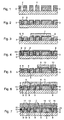
- Fig. 1 shows a p + -type silicon substrate 1, to which a p-type silicon layer 3 is epitaxially applied, into which trenches 2 are etched by means of a silicon dioxide layer 4 or other suitable material as a mask, substantially up to the silicon substrate 1 and can penetrate into this. However, smaller depths of the trenches 2 are possible.
- a sacrificial oxide may be applied to increase interfacial mobility and then removed again.
- the silicon substrate 1 and the layer 3 can both be doped with boron, wherein the dopant concentration in the layer 3 is about 1 ⁇ 10 14 to 1 ⁇ 10 18 carriers cm -3 .
- the silicon dioxide layer 4 serving as a trench mask is removed.
- a first silicon dioxide film 5 is deposited as field oxide with a layer thickness that depends on the target voltage class for the MOS transistor cell, as explained above.
- Preferred layer thicknesses are between 0.1 ⁇ m to several ⁇ m.
- a plurality of layers of, for example, thermally oxidized silicon dioxide by oxidation of the trench etched semiconductor body and deposited silicon dioxide (TEOS or LPCVD oxide) are provided for the field oxide
- the desired chamfering of the oxide or the graduated transition from gate oxide to field plate oxide results from the higher wet chemical etch rate of the LPCVD oxide over the thermal oxide.
- the thickness of the two layers is chosen so that the oxide in the trench bottom can withstand the voltage requirements of the transistor.
- an auxiliary layer 6 of, for example, photoresist is applied over the edge of the semiconductor body, cured and etched back so that only "stoppers" remain below the lower body edge in the trenches 2.
- a temperature treatment "postbake" follows.
- postbake a temperature treatment
- an additional masking can then be carried out by means of a further auxiliary layer 7 of photoresist, which is exposed and developed, whereby the field oxide 5 remains below this further auxiliary layer 7 in a subsequent etching back.
- the two trenches below the auxiliary layer 7 are so-called “inactive” trenches in contrast to the other "active” trenches.
- the inactive trenches serve, for example, for electrically connecting the gates, as gate fingers and, as already mentioned, for the edge construction.
- the two auxiliary layers 6 and 7 are then removed, that is, the photoresist is removed.
- a gate insulating film 5 'of silicon dioxide is grown, which is thinner than the first insulating film 5, so that in the trenches 2, a step ("oxide stage") 33 is formed.
- This step 33 may be chamfered when multiple layers are used for the first insulating film 5, as explained above.
- the angle of the chamfered step 20 to the vertical may be for example 17 °. Of course, other angles are possible.
- the gate insulating layer 5 ' is provided with a layer thickness of a few nm to more than 100 nm. In any case, however, the layer thickness of the gate insulating layer 5 'is less than the final thickness of the first insulating film fifth
- gate material 8 of, for example, polycrystalline silicon is deposited and doped, whereby the structure shown in FIG. 4 is obtained.
- the gate material 8 is then patterned by means of a masking layer 10 of, for example, photoresist etched back to below the silicon top edge, so that the structure shown in Fig. 5 is formed.
- a masking layer 10 of, for example, photoresist etched back to below the silicon top edge so that the structure shown in Fig. 5 is formed.
- sealing of the polycrystalline material 8 may be performed by means of, for example, a thin silicon dioxide layer, not shown in the drawings, to prevent outdiffusion of dopants from the polycrystalline material 8.
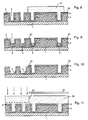
- a photoresist layer 11 with uncritical flank over the left in Fig. 6 polycrystalline material 8 and an implantation and optionally annealing of an n + -type body gain zone 12 in the region of the oxide stage 33 to the breakdown voltage of the trench MOS Lowering transistor cell below the breakdown voltage at the oxide stage 33 in the trench 2.
- the dopant concentration in this zone 12 is preferably about 1 x 10 18 charge carriers cm -3 .
- a p ++ -conducting source zone 18 and a p ++ -conducting diffusion zone 19 are introduced, masked by the field oxide or by a separate phototechnology.
- an insulating layer 17 of borophosphosilicate glass is applied, compacted and patterned by etching vias.
- a metallization (electrode) 13 for source, a metallization (electrode) 14 for gate, and a metallization 15 are deposited and patterned, eventually yielding the structure shown in FIG. 7 after passivation becomes.
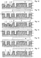
- FIG 8 to 10 show a variant of the method according to the invention, in which, after application of the first insulating film 5 and before attaching the auxiliary layer 6, a thin silicon nitride layer having a layer thickness of, for example, 20 nm is applied to the insulating film 5 (cf., FIG is patterned by means of a lacquer layer 21, so that the silicon nitride layer 20 remains only in the areas below the lacquer layer 21. This ensures that the silicon nitride layer 20 remains only in the region of the inactive trenches.
- the arrangement shown in Figure 9 is obtained in which the auxiliary layer 6 of paint stoppers remains in the trenches.
- the insulating film 5 of silicon dioxide in the trench bottoms of the active trenches is masked by the auxiliary layer 6 and the entire inactive trenches by means of the silicon nitride layer 20.
- the process result is the same as in the first embodiment before attaching the second insulating film 5 '.
- Figures 11 and 12 illustrate a third embodiment of the method according to the invention in which the structuring of the first insulating film 5 in the active trenches and the inactive trenches is carried out by means of a single phototechnique.
- a lacquer layer 23 with a layer thickness of, for example, 4 ⁇ m is exposed by means of a mask 22 only to a certain depth (cf., the dashed line 24). The exposed part of the lacquer layer 23 is removed.
- only lacquer stoppers 26 remain as auxiliary layer 6 and a lacquer layer 25 with a layer thickness of about 1.5 ⁇ m above the inactive trenches.
- This further removal process of the varnish layer 23 for obtaining the varnish stopper 26 and the varnish layer 25 can be effected, for example, by a plasma etch back (cf., FIG. 12). Instead of such a plasma etch, if desired, a dry development can also be carried out.
- FIGS. 13 and 14 show sections for illustrating a further variant of the method according to the invention in accordance with a fourth exemplary embodiment.
- a first photoresist layer 31 inactive trenches are covered while with the aid of a second photoresist layer 32 the necessary topography, i. Structuring of the first insulating film 5 is made.
- the auxiliary layer 6 in the form of paint stoppers remains in the active trenches while the inactive trenches are filled with the photoresist layer 31.
- the further processing takes place as in the first embodiment.
- FIGS. 15 to 17 show sections for explaining a further variant of the method according to the invention in a fifth exemplary embodiment, which is similar to the fourth exemplary embodiment: two phototechniques are also used here, but here a structuring method is used Photoresist layer 28 having a layer thickness of about 3 microns only after applying a photoresist layer 27 is produced with a layer thickness of about 1 micron.
- the structure thus obtained is shown in FIG. After removing substantial portions of the photoresist layer 28 and the photoresist layer 27, only photoresist layers 29 remain (as the remainder of the photoresist layer 28) and 30 (as the remainder of the photoresist layer 27) to have the arrangement shown in FIG.
Landscapes
- Insulated Gate Type Field-Effect Transistor (AREA)
- Electrodes Of Semiconductors (AREA)
- Element Separation (AREA)
Claims (15)
- Procédé de production d'un transistor de puissance MOS-Trench, dans lequel on ménage, dans un corps (1, 3) semi-conducteur, au moins un sillon (2) que l'on emplit ensuite, au moins en partie, d'une matière (8) conductrice séparée de la surface intérieure du sillon par une couche (5, 5') isolante, la couche (5, 5') isolante étant introduite dans les sillons (2) de façon à ce que qu'elle ait, dans la partie de l'extrémité inférieure du sillon (2), une épaisseur de couche plus grande que dans sa partie supérieure, comprenant les stades suivants :(a) on ménage le au moins un sillon (2) dans le corps (1, 3) semi-conducteur,(b) on met une première pellicule (5) isolante sur les parois et sur le fond du sillon,(c) on emplit l'extrémité inférieure du sillon (2) d'une première couche (6) auxiliaire,(d) on élimine les parties de la première pellicule (5) isolante, qui ne sont pas revêtues de la première couche (6) auxiliaire,(e) on élimine la couche (6) auxiliaire,(f) on fait croître, sur les parois mises à nu du sillon (2), une deuxième pellicule (5') isolante qui est plus mince que l'épaisseur finale de la première pellicule (5) isolante,(g) on emplit le sillon de la matière (8) conductrice et(h) on ménage des zones (19) de source et de body dans le corps (1, 3) semi-conducteur et on ménage des métallisations (13, 14, 15) pour la mise en contact,caractérisé en ce que(b1) dans le stade (b), on dépose la première pellicule (5) isolante en plusieurs couches oxydées thermiquement et déposées.
- Procédé suivant la revendication 1,
caractérisé en ce que l'on ménage le sillon (2) dans une couche (3) épitaxiale prévue sur un substrat (1) semi-conducteur. - Procédé suivant la revendication 1 ou 2,
caractérisé en ce que l'on munit la couche (3) épitaxiale d'une concentration de substance de dopage de 1 x 10¹⁴ à 1 x 10¹⁸ porteurs de charge cm-3. - Procédé suivant l'une des revendications 1 à 3,
caractérisé en ce qu'on ménage les sillons (2) sous forme de bandes ou de réseau dans le corps (1, 3) semi-conducteur. - Procédé suivant l'une des revendications 1 à 4,
caractérisé en ce que l'on dépose la première pellicule (5) isolante en une épaisseur d'environ 0,1 µm à quelques µm. - Procédé suivant l'une des revendications 1 à 5,
caractérisé en ce que l'on utilise un vernis photosensible pour la première couche (6) auxiliaire. - Procédé suivant l'une des revendications 1 à 6,
caractérisé en ce que l'on dépose, pour une construction de bord en tant que masquage supplémentaire, une autre couche (7) auxiliaire qui empêche l'élimination de la première pellicule (5) isolante dans les parties masquées. - Procédé suivant l'une des revendications 1 à 7,
caractérisé en ce que l'on dépose la deuxième pellicule isolante en une épaisseur de quelques nm à plus de 100 nm. - Procédé suivant l'une des revendications 1 à 8,
caractérisé en ce que l'on ménage dans la zone (9) de body un renfort (12). - Procédé suivant la revendication 9,
caractérisé en ce que l'on implante le renfort (12). - Procédé suivant l'une des revendications 1 à 10,
caractérisé en ce qu'après avoir revêtu les parois et le fond du sillon de la première pellicule (5) isolante, on dépose et on structure une couche (20) de nitrure de silicium sur la première pellicule (5) isolante. - Procédé suivant la revendication 11,
caractérisé en ce que la couche (20) de nitrure de silicium a une épaisseur d'environ 20 nm. - Procédé suivant l'une des revendications 1 à 10,
caractérisé en ce que l'on produit la couche (6 ou 26) auxiliaire et la structuration de la première pellicule (5) isolante à l'aide d'une couche (23) unique de vernis photosensible qui n'est insolée par l'intermédiaire d'un masque (22) que jusqu'à une profondeur (24) prescrite. - Procédé suivant l'une des revendications 1 à 10,
caractérisé en ce que l'on revêt des sillons inactifs au moyen d'une première couche (31) de vernis photosensible qui y est introduite et on effectue une structuration de la première pellicule (5) isolante au moyen d'une deuxième couche (32) de vernis photosensible disposée à l'extérieur de la première couche (31) de vernis photosensible. - Procédé suivant la revendication 13,
caractérisé en ce que l'on déposé la couche (32) structurante de vernis photosensible après la couche (31) recouvrante de vernis photosensible.
Applications Claiming Priority (3)
| Application Number | Priority Date | Filing Date | Title |
|---|---|---|---|
| DE19935442 | 1999-07-28 | ||
| DE19935442A DE19935442C1 (de) | 1999-07-28 | 1999-07-28 | Verfahren zum Herstellen eines Trench-MOS-Leistungstransistors |
| PCT/DE2000/001647 WO2001009956A1 (fr) | 1999-07-28 | 2000-05-23 | Procede de production d'un transistor de puissance mos a tranchees |
Publications (2)
| Publication Number | Publication Date |
|---|---|
| EP1204992A1 EP1204992A1 (fr) | 2002-05-15 |
| EP1204992B1 true EP1204992B1 (fr) | 2006-09-13 |
Family
ID=7916356
Family Applications (1)
| Application Number | Title | Priority Date | Filing Date |
|---|---|---|---|
| EP00945560A Expired - Lifetime EP1204992B1 (fr) | 1999-07-28 | 2000-05-23 | Procede de production d'un transistor de puissance mos a tranchees |
Country Status (4)
| Country | Link |
|---|---|
| US (1) | US6528355B2 (fr) |
| EP (1) | EP1204992B1 (fr) |
| DE (2) | DE19935442C1 (fr) |
| WO (1) | WO2001009956A1 (fr) |
Families Citing this family (24)
| Publication number | Priority date | Publication date | Assignee | Title |
|---|---|---|---|---|
| US6593619B1 (en) | 1999-06-03 | 2003-07-15 | General Semiconductor, Inc. | High voltage power MOSFET having low on-resistance |
| TW523816B (en) * | 2000-06-16 | 2003-03-11 | Gen Semiconductor Inc | Semiconductor trench device with enhanced gate oxide integrity structure |
| DE10127885B4 (de) | 2001-06-08 | 2009-09-24 | Infineon Technologies Ag | Trench-Leistungshalbleiterbauelement |
| US6882000B2 (en) * | 2001-08-10 | 2005-04-19 | Siliconix Incorporated | Trench MIS device with reduced gate-to-drain capacitance |
| US6635544B2 (en) * | 2001-09-07 | 2003-10-21 | Power Intergrations, Inc. | Method of fabricating a high-voltage transistor with a multi-layered extended drain structure |
| US6674124B2 (en) * | 2001-11-15 | 2004-01-06 | General Semiconductor, Inc. | Trench MOSFET having low gate charge |
| JP3673231B2 (ja) | 2002-03-07 | 2005-07-20 | 三菱電機株式会社 | 絶縁ゲート型半導体装置及びゲート配線構造の製造方法 |
| DE10324754B4 (de) | 2003-05-30 | 2018-11-08 | Infineon Technologies Ag | Halbleiterbauelement |
| DE102004009083B4 (de) * | 2004-02-25 | 2008-08-07 | Infineon Technologies Ag | MOS-Leistungstransistoranordnung und Verfahren zu deren Herstellung |
| GB0405325D0 (en) | 2004-03-10 | 2004-04-21 | Koninkl Philips Electronics Nv | Trench-gate transistors and their manufacture |
| US7087959B2 (en) * | 2004-08-18 | 2006-08-08 | Agere Systems Inc. | Metal-oxide-semiconductor device having an enhanced shielding structure |
| US7390756B2 (en) * | 2005-04-28 | 2008-06-24 | Micron Technology, Inc. | Atomic layer deposited zirconium silicon oxide films |
| EP1742257B1 (fr) * | 2005-07-08 | 2012-09-05 | STMicroelectronics Srl | Méthode de fabrication d'un dispositif semi-conducteur de puissance |
| ITTO20050630A1 (it) * | 2005-09-15 | 2007-03-16 | St Microelectronics Srl | Dispositivo di potenza a semiconduttore a porta isolata formata in uno scavo e relativo procedimento di fabbricazione |
| DE102005052733B3 (de) * | 2005-11-04 | 2007-05-03 | Infineon Technologies Ag | Vertikales Halbleiterbauelement |
| US7880201B2 (en) * | 2006-11-09 | 2011-02-01 | International Business Machines Corporation | Optical modulator using a serpentine dielectric layer between silicon layers |
| DE102007014038B4 (de) | 2007-03-23 | 2015-02-12 | Infineon Technologies Austria Ag | Verfahren zur Herstellung eines Halbleiterbauelements |
| US7615847B2 (en) * | 2007-03-23 | 2009-11-10 | Infineon Technologies Austria Ag | Method for producing a semiconductor component |
| JP5183959B2 (ja) * | 2007-04-23 | 2013-04-17 | 新日本無線株式会社 | Mosfet型半導体装置の製造方法 |
| US8664713B2 (en) | 2008-12-31 | 2014-03-04 | Stmicroelectronics S.R.L. | Integrated power device on a semiconductor substrate having an improved trench gate structure |
| IT1396561B1 (it) * | 2009-03-13 | 2012-12-14 | St Microelectronics Srl | Metodo per realizzare un dispositivo di potenza con struttura trench-gate e relativo dispositivo |
| DE102015103211B4 (de) | 2015-03-05 | 2018-05-30 | Infineon Technologies Austria Ag | Verfahren zum herstellen einer halbleitervorrichtung mit ersten und zweiten feldelektrodenstrukturen |
| WO2021254616A1 (fr) * | 2020-06-18 | 2021-12-23 | Dynex Semiconductor Limited | Mosfet au sic à oxyde de tranchée asymétrique et procédé de fabrication |
| EP4672906A1 (fr) * | 2024-06-28 | 2025-12-31 | Nexperia B.V. | Procédé de fabrication d'oxyde épais inférieur (bto) dans une tranchée d'un matériau semi-conducteur ainsi qu'oxyde de champ (fox) sur le matériau semi-conducteur |
Family Cites Families (11)
| Publication number | Priority date | Publication date | Assignee | Title |
|---|---|---|---|---|
| US4941026A (en) * | 1986-12-05 | 1990-07-10 | General Electric Company | Semiconductor devices exhibiting minimum on-resistance |
| US4914058A (en) * | 1987-12-29 | 1990-04-03 | Siliconix Incorporated | Grooved DMOS process with varying gate dielectric thickness |
| US5283201A (en) * | 1988-05-17 | 1994-02-01 | Advanced Power Technology, Inc. | High density power device fabrication process |
| US5430324A (en) * | 1992-07-23 | 1995-07-04 | Siliconix, Incorporated | High voltage transistor having edge termination utilizing trench technology |
| US5326711A (en) * | 1993-01-04 | 1994-07-05 | Texas Instruments Incorporated | High performance high voltage vertical transistor and method of fabrication |
| JP3396553B2 (ja) * | 1994-02-04 | 2003-04-14 | 三菱電機株式会社 | 半導体装置の製造方法及び半導体装置 |
| US5424231A (en) * | 1994-08-09 | 1995-06-13 | United Microelectronics Corp. | Method for manufacturing a VDMOS transistor |
| US6049108A (en) * | 1995-06-02 | 2000-04-11 | Siliconix Incorporated | Trench-gated MOSFET with bidirectional voltage clamping |
| WO1997007548A1 (fr) * | 1995-08-21 | 1997-02-27 | Siliconix Incorporated | Transistor mos a double diffusion en tranchees a canal court basse tension |
| US5637898A (en) * | 1995-12-22 | 1997-06-10 | North Carolina State University | Vertical field effect transistors having improved breakdown voltage capability and low on-state resistance |
| JP4077529B2 (ja) * | 1996-05-22 | 2008-04-16 | フェアチャイルドコリア半導体株式会社 | トレンチ拡散mosトランジスタの製造方法 |
-
1999
- 1999-07-28 DE DE19935442A patent/DE19935442C1/de not_active Expired - Fee Related
-
2000
- 2000-05-23 EP EP00945560A patent/EP1204992B1/fr not_active Expired - Lifetime
- 2000-05-23 WO PCT/DE2000/001647 patent/WO2001009956A1/fr not_active Ceased
- 2000-05-23 DE DE50013469T patent/DE50013469D1/de not_active Expired - Lifetime
-
2002
- 2002-01-28 US US10/058,526 patent/US6528355B2/en not_active Expired - Lifetime
Also Published As
| Publication number | Publication date |
|---|---|
| WO2001009956A1 (fr) | 2001-02-08 |
| US6528355B2 (en) | 2003-03-04 |
| DE19935442C1 (de) | 2000-12-21 |
| US20020094635A1 (en) | 2002-07-18 |
| EP1204992A1 (fr) | 2002-05-15 |
| DE50013469D1 (de) | 2006-10-26 |
Similar Documents
| Publication | Publication Date | Title |
|---|---|---|
| EP1204992B1 (fr) | Procede de production d'un transistor de puissance mos a tranchees | |
| DE69209678T2 (de) | Halbleiteranordnung für Hochspannungsverwendung und Verfahren zur Herstellung | |
| DE60035144T2 (de) | MOS-Gate-Leistungsbauelement hoher Dichte und dessen Herstellungsverfahren | |
| DE69535441T2 (de) | Verfahren zur herstellung eines mos gesteuerten bauelements mit reduzierter maskenzahl | |
| DE102008055689B4 (de) | Siliziumkarbid-Halbleitervorrichtung und Herstellungsverfahren hierfür | |
| DE102014117780B4 (de) | Halbleiterbauelement mit einer Grabenelektrode und Verfahren zur Herstellung | |
| DE69307216T2 (de) | Verfahren für DMOS-Transistor mit Grabenstruktur unter Verwendung von sechs Masken | |
| EP1151478B1 (fr) | Composant de puissance mos et procede de fabrication dudit composant | |
| DE19949364B4 (de) | Halbleiterbauteil mit MOS-Gate-Steuerung und Grabenstruktur sowie Verfahren zur Herstellung | |
| DE69434643T2 (de) | Struktur und Herstellung von Leistungs-MOSFET unter Einbeziehung der Struktur des Randes | |
| DE4011276C2 (de) | Feldeffekttransistor mit isoliertem Gate (IGFET) und Verfahren zu seiner Herstellung | |
| DE10196441B4 (de) | Verfahren zur Herstellung eines MOSFET | |
| DE19535140A1 (de) | Lateraler MOSFET mit hoher Stehspannung und einem Graben sowie Verfahren zu dessen Herstellung | |
| DE10296970B4 (de) | Halbleitervorrichtung und Verfahren zur Herstellung derselben | |
| DE19747159A1 (de) | Halbleiterbauteil mit MOS-Gatesteuerung und Verfahren zu seiner Herstellung | |
| DE102005052731A1 (de) | Siliziumkarbidhalbleitervorrichtung und Verfahren zur Herstellung derselben | |
| DE2502235A1 (de) | Ladungskopplungs-halbleiteranordnung | |
| DE102009002813B4 (de) | Verfahren zur Herstellung eines Transistorbauelements mit einer Feldplatte | |
| DE10234996B4 (de) | Verfahren zur Herstellung einer Transistoranordnung mit Trench-Transistorzellen mit Feldelektrode | |
| DE19507146C2 (de) | Halbleitervorrichtung und Verfahren zu deren Herstellung | |
| DE102004057791B4 (de) | Trenchtransistor sowie Verfahren zu dessen Herstellung | |
| DE69924338T2 (de) | Verfahren zur herstellung von halbleiterbauelementen mit einem graben-gate | |
| DE10129289A1 (de) | Halbleitervorrichtung mit einer Diode für eine Eingangschutzschaltung einer MOS-Vorrichtung und Verfahren zu deren Herstellung | |
| DE19641838A1 (de) | Abschlußstruktur für Halbleiterbauteile sowie Verfahren zur Herstellung derartiger Abschlußstrukturen | |
| DE19750221B4 (de) | Verfahren zu Herstellung eines Halbleiterbauteils mit MOS-Gatesteuerung |
Legal Events
| Date | Code | Title | Description |
|---|---|---|---|
| PUAI | Public reference made under article 153(3) epc to a published international application that has entered the european phase |
Free format text: ORIGINAL CODE: 0009012 |
|
| 17P | Request for examination filed |
Effective date: 20011210 |
|
| AK | Designated contracting states |
Kind code of ref document: A1 Designated state(s): AT BE CH CY DE DK ES FI FR GB GR IE IT LI LU MC NL PT SE |
|
| RBV | Designated contracting states (corrected) |
Designated state(s): DE FR IT |
|
| GRAP | Despatch of communication of intention to grant a patent |
Free format text: ORIGINAL CODE: EPIDOSNIGR1 |
|
| GRAS | Grant fee paid |
Free format text: ORIGINAL CODE: EPIDOSNIGR3 |
|
| GRAA | (expected) grant |
Free format text: ORIGINAL CODE: 0009210 |
|
| AK | Designated contracting states |
Kind code of ref document: B1 Designated state(s): DE FR IT |
|
| PG25 | Lapsed in a contracting state [announced via postgrant information from national office to epo] |
Ref country code: IT Free format text: LAPSE BECAUSE OF FAILURE TO SUBMIT A TRANSLATION OF THE DESCRIPTION OR TO PAY THE FEE WITHIN THE PRESCRIBED TIME-LIMIT;WARNING: LAPSES OF ITALIAN PATENTS WITH EFFECTIVE DATE BEFORE 2007 MAY HAVE OCCURRED AT ANY TIME BEFORE 2007. THE CORRECT EFFECTIVE DATE MAY BE DIFFERENT FROM THE ONE RECORDED. Effective date: 20060913 |
|
| REF | Corresponds to: |
Ref document number: 50013469 Country of ref document: DE Date of ref document: 20061026 Kind code of ref document: P |
|
| ET | Fr: translation filed | ||
| PLBE | No opposition filed within time limit |
Free format text: ORIGINAL CODE: 0009261 |
|
| STAA | Information on the status of an ep patent application or granted ep patent |
Free format text: STATUS: NO OPPOSITION FILED WITHIN TIME LIMIT |
|
| 26N | No opposition filed |
Effective date: 20070614 |
|
| REG | Reference to a national code |
Ref country code: FR Ref legal event code: PLFP Year of fee payment: 17 |
|
| REG | Reference to a national code |
Ref country code: FR Ref legal event code: PLFP Year of fee payment: 18 |
|
| REG | Reference to a national code |
Ref country code: FR Ref legal event code: PLFP Year of fee payment: 19 |
|
| PGFP | Annual fee paid to national office [announced via postgrant information from national office to epo] |
Ref country code: IT Payment date: 20180530 Year of fee payment: 19 Ref country code: FR Payment date: 20180522 Year of fee payment: 19 |
|
| PGFP | Annual fee paid to national office [announced via postgrant information from national office to epo] |
Ref country code: DE Payment date: 20180716 Year of fee payment: 19 |
|
| REG | Reference to a national code |
Ref country code: DE Ref legal event code: R119 Ref document number: 50013469 Country of ref document: DE |
|
| PG25 | Lapsed in a contracting state [announced via postgrant information from national office to epo] |
Ref country code: IT Free format text: LAPSE BECAUSE OF NON-PAYMENT OF DUE FEES Effective date: 20190523 Ref country code: DE Free format text: LAPSE BECAUSE OF NON-PAYMENT OF DUE FEES Effective date: 20191203 |
|
| PG25 | Lapsed in a contracting state [announced via postgrant information from national office to epo] |
Ref country code: FR Free format text: LAPSE BECAUSE OF NON-PAYMENT OF DUE FEES Effective date: 20190531 |