EP1205784A2 - Lichtmodulator mit mehrfachen Quantentöpfen - Google Patents
Lichtmodulator mit mehrfachen Quantentöpfen Download PDFInfo
- Publication number
- EP1205784A2 EP1205784A2 EP01118651A EP01118651A EP1205784A2 EP 1205784 A2 EP1205784 A2 EP 1205784A2 EP 01118651 A EP01118651 A EP 01118651A EP 01118651 A EP01118651 A EP 01118651A EP 1205784 A2 EP1205784 A2 EP 1205784A2
- Authority
- EP
- European Patent Office
- Prior art keywords
- quantum well
- multiple quantum
- inp
- intensity
- substrate
- Prior art date
- Legal status (The legal status is an assumption and is not a legal conclusion. Google has not performed a legal analysis and makes no representation as to the accuracy of the status listed.)
- Withdrawn
Links
Images


Classifications
-
- G—PHYSICS
- G02—OPTICS
- G02F—OPTICAL DEVICES OR ARRANGEMENTS FOR THE CONTROL OF LIGHT BY MODIFICATION OF THE OPTICAL PROPERTIES OF THE MEDIA OF THE ELEMENTS INVOLVED THEREIN; NON-LINEAR OPTICS; FREQUENCY-CHANGING OF LIGHT; OPTICAL LOGIC ELEMENTS; OPTICAL ANALOGUE/DIGITAL CONVERTERS
- G02F1/00—Devices or arrangements for the control of the intensity, colour, phase, polarisation or direction of light arriving from an independent light source, e.g. switching, gating or modulating; Non-linear optics
- G02F1/01—Devices or arrangements for the control of the intensity, colour, phase, polarisation or direction of light arriving from an independent light source, e.g. switching, gating or modulating; Non-linear optics for the control of the intensity, phase, polarisation or colour
- G02F1/015—Devices or arrangements for the control of the intensity, colour, phase, polarisation or direction of light arriving from an independent light source, e.g. switching, gating or modulating; Non-linear optics for the control of the intensity, phase, polarisation or colour based on semiconductor elements having potential barriers, e.g. having a PN or PIN junction
- G02F1/017—Structures with periodic or quasi periodic potential variation, e.g. superlattices, quantum wells
-
- B—PERFORMING OPERATIONS; TRANSPORTING
- B82—NANOTECHNOLOGY
- B82Y—SPECIFIC USES OR APPLICATIONS OF NANOSTRUCTURES; MEASUREMENT OR ANALYSIS OF NANOSTRUCTURES; MANUFACTURE OR TREATMENT OF NANOSTRUCTURES
- B82Y20/00—Nanooptics, e.g. quantum optics or photonic crystals
-
- G—PHYSICS
- G02—OPTICS
- G02B—OPTICAL ELEMENTS, SYSTEMS OR APPARATUS
- G02B6/00—Light guides; Structural details of arrangements comprising light guides and other optical elements, e.g. couplings
- G02B6/10—Light guides; Structural details of arrangements comprising light guides and other optical elements, e.g. couplings of the optical waveguide type
- G02B6/12—Light guides; Structural details of arrangements comprising light guides and other optical elements, e.g. couplings of the optical waveguide type of the integrated circuit kind
- G02B2006/12133—Functions
- G02B2006/12142—Modulator
-
- G—PHYSICS
- G02—OPTICS
- G02F—OPTICAL DEVICES OR ARRANGEMENTS FOR THE CONTROL OF LIGHT BY MODIFICATION OF THE OPTICAL PROPERTIES OF THE MEDIA OF THE ELEMENTS INVOLVED THEREIN; NON-LINEAR OPTICS; FREQUENCY-CHANGING OF LIGHT; OPTICAL LOGIC ELEMENTS; OPTICAL ANALOGUE/DIGITAL CONVERTERS
- G02F1/00—Devices or arrangements for the control of the intensity, colour, phase, polarisation or direction of light arriving from an independent light source, e.g. switching, gating or modulating; Non-linear optics
- G02F1/01—Devices or arrangements for the control of the intensity, colour, phase, polarisation or direction of light arriving from an independent light source, e.g. switching, gating or modulating; Non-linear optics for the control of the intensity, phase, polarisation or colour
- G02F1/015—Devices or arrangements for the control of the intensity, colour, phase, polarisation or direction of light arriving from an independent light source, e.g. switching, gating or modulating; Non-linear optics for the control of the intensity, phase, polarisation or colour based on semiconductor elements having potential barriers, e.g. having a PN or PIN junction
- G02F1/017—Structures with periodic or quasi periodic potential variation, e.g. superlattices, quantum wells
- G02F1/01766—Strained superlattice devices; Strained quantum well devices
-
- G—PHYSICS
- G02—OPTICS
- G02F—OPTICAL DEVICES OR ARRANGEMENTS FOR THE CONTROL OF LIGHT BY MODIFICATION OF THE OPTICAL PROPERTIES OF THE MEDIA OF THE ELEMENTS INVOLVED THEREIN; NON-LINEAR OPTICS; FREQUENCY-CHANGING OF LIGHT; OPTICAL LOGIC ELEMENTS; OPTICAL ANALOGUE/DIGITAL CONVERTERS
- G02F2202/00—Materials and properties
- G02F2202/10—Materials and properties semiconductor
- G02F2202/102—In×P and alloy
-
- G—PHYSICS
- G02—OPTICS
- G02F—OPTICAL DEVICES OR ARRANGEMENTS FOR THE CONTROL OF LIGHT BY MODIFICATION OF THE OPTICAL PROPERTIES OF THE MEDIA OF THE ELEMENTS INVOLVED THEREIN; NON-LINEAR OPTICS; FREQUENCY-CHANGING OF LIGHT; OPTICAL LOGIC ELEMENTS; OPTICAL ANALOGUE/DIGITAL CONVERTERS
- G02F2203/00—Function characteristic
- G02F2203/02—Function characteristic reflective
-
- H—ELECTRICITY
- H10—SEMICONDUCTOR DEVICES; ELECTRIC SOLID-STATE DEVICES NOT OTHERWISE PROVIDED FOR
- H10P—GENERIC PROCESSES OR APPARATUS FOR THE MANUFACTURE OR TREATMENT OF DEVICES COVERED BY CLASS H10
- H10P14/00—Formation of materials, e.g. in the shape of layers or pillars
- H10P14/20—Formation of materials, e.g. in the shape of layers or pillars of semiconductor materials
- H10P14/29—Formation of materials, e.g. in the shape of layers or pillars of semiconductor materials characterised by the substrates
- H10P14/2901—Materials
- H10P14/2907—Materials being Group IIIA-VA materials
- H10P14/2909—Phosphides
-
- H—ELECTRICITY
- H10—SEMICONDUCTOR DEVICES; ELECTRIC SOLID-STATE DEVICES NOT OTHERWISE PROVIDED FOR
- H10P—GENERIC PROCESSES OR APPARATUS FOR THE MANUFACTURE OR TREATMENT OF DEVICES COVERED BY CLASS H10
- H10P14/00—Formation of materials, e.g. in the shape of layers or pillars
- H10P14/20—Formation of materials, e.g. in the shape of layers or pillars of semiconductor materials
- H10P14/32—Formation of materials, e.g. in the shape of layers or pillars of semiconductor materials characterised by intermediate layers between substrates and deposited layers
- H10P14/3202—Materials thereof
- H10P14/3214—Materials thereof being Group IIIA-VA semiconductors
- H10P14/3218—Phosphides
-
- H—ELECTRICITY
- H10—SEMICONDUCTOR DEVICES; ELECTRIC SOLID-STATE DEVICES NOT OTHERWISE PROVIDED FOR
- H10P—GENERIC PROCESSES OR APPARATUS FOR THE MANUFACTURE OR TREATMENT OF DEVICES COVERED BY CLASS H10
- H10P14/00—Formation of materials, e.g. in the shape of layers or pillars
- H10P14/20—Formation of materials, e.g. in the shape of layers or pillars of semiconductor materials
- H10P14/32—Formation of materials, e.g. in the shape of layers or pillars of semiconductor materials characterised by intermediate layers between substrates and deposited layers
- H10P14/3202—Materials thereof
- H10P14/3214—Materials thereof being Group IIIA-VA semiconductors
- H10P14/3221—Arsenides
-
- H—ELECTRICITY
- H10—SEMICONDUCTOR DEVICES; ELECTRIC SOLID-STATE DEVICES NOT OTHERWISE PROVIDED FOR
- H10P—GENERIC PROCESSES OR APPARATUS FOR THE MANUFACTURE OR TREATMENT OF DEVICES COVERED BY CLASS H10
- H10P14/00—Formation of materials, e.g. in the shape of layers or pillars
- H10P14/20—Formation of materials, e.g. in the shape of layers or pillars of semiconductor materials
- H10P14/32—Formation of materials, e.g. in the shape of layers or pillars of semiconductor materials characterised by intermediate layers between substrates and deposited layers
- H10P14/3242—Structure
- H10P14/3244—Layer structure
- H10P14/3251—Layer structure consisting of three or more layers
- H10P14/3252—Alternating layers, e.g. superlattice
-
- H—ELECTRICITY
- H10—SEMICONDUCTOR DEVICES; ELECTRIC SOLID-STATE DEVICES NOT OTHERWISE PROVIDED FOR
- H10P—GENERIC PROCESSES OR APPARATUS FOR THE MANUFACTURE OR TREATMENT OF DEVICES COVERED BY CLASS H10
- H10P14/00—Formation of materials, e.g. in the shape of layers or pillars
- H10P14/20—Formation of materials, e.g. in the shape of layers or pillars of semiconductor materials
- H10P14/34—Deposited materials, e.g. layers
- H10P14/3402—Deposited materials, e.g. layers characterised by the chemical composition
- H10P14/3414—Deposited materials, e.g. layers characterised by the chemical composition being group IIIA-VIA materials
- H10P14/3418—Phosphides
-
- H—ELECTRICITY
- H10—SEMICONDUCTOR DEVICES; ELECTRIC SOLID-STATE DEVICES NOT OTHERWISE PROVIDED FOR
- H10P—GENERIC PROCESSES OR APPARATUS FOR THE MANUFACTURE OR TREATMENT OF DEVICES COVERED BY CLASS H10
- H10P14/00—Formation of materials, e.g. in the shape of layers or pillars
- H10P14/20—Formation of materials, e.g. in the shape of layers or pillars of semiconductor materials
- H10P14/34—Deposited materials, e.g. layers
- H10P14/3402—Deposited materials, e.g. layers characterised by the chemical composition
- H10P14/3414—Deposited materials, e.g. layers characterised by the chemical composition being group IIIA-VIA materials
- H10P14/3421—Arsenides
-
- Y—GENERAL TAGGING OF NEW TECHNOLOGICAL DEVELOPMENTS; GENERAL TAGGING OF CROSS-SECTIONAL TECHNOLOGIES SPANNING OVER SEVERAL SECTIONS OF THE IPC; TECHNICAL SUBJECTS COVERED BY FORMER USPC CROSS-REFERENCE ART COLLECTIONS [XRACs] AND DIGESTS
- Y10—TECHNICAL SUBJECTS COVERED BY FORMER USPC
- Y10S—TECHNICAL SUBJECTS COVERED BY FORMER USPC CROSS-REFERENCE ART COLLECTIONS [XRACs] AND DIGESTS
- Y10S438/00—Semiconductor device manufacturing: process
- Y10S438/938—Lattice strain control or utilization
Definitions
- the present invention relates to an accurate in-situ growth technique based upon reflection high energy electron diffraction dynamics for accurate lattice matching of dissimilar materials.
- optical fibers for use as a practical optical transmission medium have stimulated tremendous growth in other areas relating to optical communications.
- optical refers not only to visible light but to any electromagnetic radiation which can be transmitted within dielectric fibers.
- the term refers to electromagnetic radiation generally of wavelength between 0.1 and 50 microns.
- fiber to the home systems have been proposed which would utilize surface normal electroabsorption modulators to convert downstream light into upstream data.
- One such, system uses a single fiber to connect two locations and effects bidirectional data transmission over this fiber using a single laser. See, e.g., T. Wood et al., Elec. Lett., Vol. 22, pgs. 346-352 (1986) and T. Wood et al., J.
- the MQW includes a plurality of layers of different semiconductor materials such as gallium arsenide (GaAs) and aluminum gallium arsenide (AlGaAs).
- suitable materials include such III-V systems as InAs/GaAs,(In,Ga)As/GaAs, (In,Ga)As/InP and (In,Ga)As/(In,Al)As.
- the layers alternate between wide bandgap material and narrow bandgap material. Appropriate selection of materials, compositions and layer thicknesses permits fabrication of unique electrooptic devices.
- the MQW When used as a modulator, the MQW exhibits a significant shift in the absorption edge due to the change in the confinement energy associated with the applied electric field and consequent distortion of the well. This shift in absorption is the basis for the MQW as a modulator. Since the applied field can significantly alter the light absorption properties of a properly biased MQW, light passing through the MQW will be modulated.
- MBE molecular beam epitaxy
- EP-A-0 420 749 discloses a device in the form of an InP p-n diode having a multiple quantum well structure between the p and n layers and consisting of an InP layer and an InGaAs well layer as an active layer.
- US-A-5,091,335 shows a process for controlling the lattice matching of III-V semiconductor films grown on different substrates by using RHEED which assesses the stoichiometry and morphology pf the depositing film.
- An in-situ method for highly accurate lattice matching using reflection high energy electron diffraction dynamics.
- the method includes the steps of providing a substrate of a first semiconductor material and initiating growth of a second semiconductor material thereon.
- the oscillation amplitude of intensity I of waveform cycles is monitored using reflection high energy electron diffraction.
- a maximum intensity I + and a minimum intensity I is determined over a predetermined number of waveform cycles.
- the fluxes of the second semiconductor material are then adjusted to maximize FM and optimize lattice matching.
- a multiple quantum well light modulator including a semiconductor substrate of InP, a multiple quantum well region, disposed above the InP substrate, composed of InGaAs and having a thickness of about 4 ⁇ m.
- the modulator is characterized by a lattice mismatch of less than 2 x 10 -4 .
- FIG. 1 is a schematic drawing of a preferred embodiment of a measurement test set up, shown generally at 20 for use with the invention as applied to a modulator.
- Surface normal modulators are attractive candidates for fiber to the home applications where their amenability to processing in large two dimensional arrays would help keep unit costs down. In order to be useful, however, contrast and absorption values must be acceptable in the 1.3 to 1.55 ⁇ m regime corresponding to the low loss, low dispersion windows for optical fibers.
- an in-situ growth approach based on RHEED dynamics is disclosed that allows InGaAs to be accurately lattice matched to an InP substrate.
- This approach is based on an analysis of the intensity oscillation amplitude as opposed to conventional approaches wherein growth rates are determined by an analysis of oscillation frequency.
- the measurement system 20 shown in FIG. 1 illustrates incident light 22 from a 0.25 Spex monochromator 23 focused through the substrate 24 onto a top metal contact 26 which serves as a metallic mirror. As shown herein the metal contact 26 is made of Au.
- the returning light beam 28 passes through a beam splitter 30 to a detector 32.
- Fig. 2 shows a plot of the intensity oscillation of RHEED when lattice matching conditions vary under a controlled change in In and Ga fluxes. Accurate lattice matching conditions are shown in Fig. 2 as clearly defined oscillations. But for slight mismatches, the RHEED oscillation amplitude is degraded both for Ga and In rich lattice mismatches. Even though the intensity oscillation amplitude has significantly changed (because of the mismatch) the oscillation frequency does not show a reproducible change. In fact, it is not possible to detect a change in oscillation frequency with reliability to better than 1%.
- Fig. 3 is a plot of the variation in oscillation amplitude for a systematic change in lattice mismatch.
- the structures were grown by Gas Source MBE in a VG-80HMBE system modified to handle gas flow. Pure AsH 3 and PH 3 constituted the Group V fluxes, while elemental Ga and In were used as the Group III sources.
- a standard VG electron gun, operated at 15 KV with a filament current of 2.25 A is used to generate the RHEED pattern.
- the image that is generated on the phosphor screen is captured with a CCD camera which sends it to a TV monitor and also to a frame grabber card capable of 256 bit resolution located in a 486 desktop PC for display on the video monitor.
- the card is capable of sampling the image 30 times a second. Software written for this card allows the user to define boxes of different pixel sizes which function as a detector.
- RHEED intensity oscillations By aligning the pixel box over a diffraction pattern feature RHEED intensity oscillations can be recorded. Further, since the position of this box once defined, remains fixed, this allows us to correct for any lateral drift in the diffraction geometries.
- a typical calibration run consists of recording the RHEED oscillations, and then transporting the data file to a program which allows us to perform both time and frequency domain analysis on the acquired data set. Using this setup a variance on the order of 1% in the growth rate between consecutive measurements can be achieved.
- FIG. 4 shows RHEED Intensity oscillations for growth very close to lattice match conditions.
- Plot B the oscillations observed for InP growth on InP are the usual type expected for binary III-V growth.
- InP exhibits sinusoidal oscillations at the periodicity of the monolayer growth rate.
- Initial cycles of the intensity oscillations are rapidly damped symmetrically about maximum and minimum surface disorder as time approaches a terminal configuration of equilibrium surface roughness. Oscillations eventually vanish when rate of formation of surface step density (i.e., spontaneous nucleation from growth) becomes comparable to the rate of 2-D ledge motion (i.e., steps on terraces coalescence to the step ledge).
- the recovery dynamics when measured with no In deposition, also exhibit typical behavior as evidenced by step coalescence dynamics which is single stage. This corresponding to an island size that grows in time.
- Final RHEED intensity after complete recovery equals initial intensity before deposition.
- FIG. 4A A Fast Fourier Transforms of the InP on InP RHEED oscillations is shown by Fig. 4A.
- the growth rate is Fourier Transform Limited 0.756 ML/s (center of the distribution) with a Full Width Half Maximum of 0.17 ML/s.
- ⁇ / ⁇ By sampling the growth rate for an effective time of 6.0 s leads to an uncertainty in growth rate ⁇ / ⁇ is huge and impractical as a means to achieve lattice matching conditions.
- the initial state of InGaAs on InP growth oscillations that exhibit asymmetrical damping characteristics. They depict initial damping of growth oscillations from configurations of maximum and minimum surface disorder that clearly differ from the symmetrical case observed for InP growth.
- the recovery dynamics for InGaAs on InP show distinct differences from InP recovery in two ways. First, time evolution in recovery dynamics is complex with evidence of multiple components present. Secondly, terminal intensity after recovery is significantly lower than initial InP intensity. All three differences appear to associate with increased surface step disorder that is associated with mismatched growth. In essence, because of the difference in areal monolayer density of the mismatched flux with the substrate additional surface steps are created to conserve total surface area. The surface steps from mismatched growth are additive to those normally generated by spontaneous nucleation during growth.
- the first few cycles of asymmetrical damping show that the surface steps from the mismatch are rapidly formed within the first four monolayers deposited. Also, the multicomponent recovery characteristics and lower total surface reflectivity correspond to island coalescence to a new configuration of surface steps on InP because of the mismatched growth.
- FM is constructed for the initial oscillation quality to be the sum of (I + -I - )/ ⁇ I over the first four consecutive ML cycles.
- I + (I - ) correspond to maximum (minimum) intensity of each waveform cycle whereas ⁇ I is the intensity drop from initial InP reflectivity to minimum reflectivity of the oscillation waveform.
- Fig. 4 shows that the FM drops by a factor four from InP growth on InP to InGaAs growth in InP.
- the FM for InGaAs on InGaAs is 20% larger than InGaAs on InP because mismatched surface steps remain from the first sequence of InGaAs deposition on InP.
- InP intensity is 25% larger than recovered intensity after first InGaAs deposition.
- Recovered intensity after second InGaAs deposition equals recovered intensity after first InGaAs deposition.
- Plot A shows RHEED oscillations observed for different InGaAs mismatches on InP. This sequence was obtained by holding the In deposition rate fixed while varying the Ga growth rate from Ga rich to In rich conditions. The variation in Ga temperature spans a range of lattice mismatch of 1/103. Clearly, RHEED intensity during InGaAs deposition show systematic difference in the oscillation quality, recovery characteristics and intensity response. From the plot, a Ga cell temperature of 910.0 C is very close to lattice matched conditions.
- the FM is shown over the same range of mismatch at finer step size than the coarse display of Plot A.
- the FM is highly sensitive to mismatch and is strongly peaked toward a lattice matching condition.
- the degradation in FM versus mismatch is symmetrical about Ga and In rich conditions with shape reminiscent of quality characteristics obtained by PL or X-ray diffraction measurements.
- FIG. 5 A typical HRXD scan of a p-i-n modulator incorporating 225 InGaAs/ InP MQW's in the intrinsic region is shown in FIG. 5.
- the average lattice mismatch is obtained by determining the angular separation between the zeroth order peak (which corresponds to the reflection from the layer with the average lattice parameter of the super lattice stack) and the reflection from the substrate peak.
- Table-1 the values of linewidth as determined from 77Kpl measurements are presented along with the mismatch values as determined from the HRXD measurement.
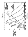
- the reflectivity spectrum over an applied reverse bias range of 0 to 50 V is plotted.
- the half width half maximum (HWHM) of the zero applied bias exciton peak is 6.2 meV and the whole spectrum shows a good quantum confined stark effect (QCSE), with the peak shifting by more than 50 nm without significant broadening over the entire applied voltage range.
- HWHM half width half maximum
- QCSE quantum confined stark effect
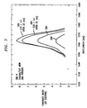
- FIGS. 7 and 8 the contrast ratios for the normally off and normally on states calculated from the reflection spectra are shown.
- a high contrast ratio of better than 8:1 is achieved by operating the exciton resonance at an applied reverse bias of 50 V.
- the bandwidth for greater than 3:1 contrast ratio, obtained at lower drive voltages is over 20 nm for both ⁇ 0 and ⁇ 1 modes of operation.
Landscapes
- Physics & Mathematics (AREA)
- Chemical & Material Sciences (AREA)
- Nonlinear Science (AREA)
- Optics & Photonics (AREA)
- Nanotechnology (AREA)
- Engineering & Computer Science (AREA)
- Crystallography & Structural Chemistry (AREA)
- Biophysics (AREA)
- General Physics & Mathematics (AREA)
- Life Sciences & Earth Sciences (AREA)
- Physical Deposition Of Substances That Are Components Of Semiconductor Devices (AREA)
- Optical Modulation, Optical Deflection, Nonlinear Optics, Optical Demodulation, Optical Logic Elements (AREA)
- Recrystallisation Techniques (AREA)
- Lasers (AREA)
- Crystals, And After-Treatments Of Crystals (AREA)
Applications Claiming Priority (3)
| Application Number | Priority Date | Filing Date | Title |
|---|---|---|---|
| US08/263,305 US5480813A (en) | 1994-06-21 | 1994-06-21 | Accurate in-situ lattice matching by reflection high energy electron diffraction |
| US263305 | 1994-06-21 | ||
| EP95304091A EP0689230B1 (de) | 1994-06-21 | 1995-06-14 | Verfahren zum gitterangepassten Aufwachsen von Halbleiterschichten |
Related Parent Applications (1)
| Application Number | Title | Priority Date | Filing Date |
|---|---|---|---|
| EP95304091A Division EP0689230B1 (de) | 1994-06-21 | 1995-06-14 | Verfahren zum gitterangepassten Aufwachsen von Halbleiterschichten |
Publications (1)
| Publication Number | Publication Date |
|---|---|
| EP1205784A2 true EP1205784A2 (de) | 2002-05-15 |
Family
ID=23001222
Family Applications (2)
| Application Number | Title | Priority Date | Filing Date |
|---|---|---|---|
| EP95304091A Expired - Lifetime EP0689230B1 (de) | 1994-06-21 | 1995-06-14 | Verfahren zum gitterangepassten Aufwachsen von Halbleiterschichten |
| EP01118651A Withdrawn EP1205784A2 (de) | 1994-06-21 | 1995-06-14 | Lichtmodulator mit mehrfachen Quantentöpfen |
Family Applications Before (1)
| Application Number | Title | Priority Date | Filing Date |
|---|---|---|---|
| EP95304091A Expired - Lifetime EP0689230B1 (de) | 1994-06-21 | 1995-06-14 | Verfahren zum gitterangepassten Aufwachsen von Halbleiterschichten |
Country Status (5)
| Country | Link |
|---|---|
| US (2) | US5480813A (de) |
| EP (2) | EP0689230B1 (de) |
| JP (1) | JP3136255B2 (de) |
| CA (1) | CA2149066C (de) |
| DE (1) | DE69525566T2 (de) |
Families Citing this family (18)
| Publication number | Priority date | Publication date | Assignee | Title |
|---|---|---|---|---|
| US5480813A (en) * | 1994-06-21 | 1996-01-02 | At&T Corp. | Accurate in-situ lattice matching by reflection high energy electron diffraction |
| US6922426B2 (en) | 2001-12-20 | 2005-07-26 | Finisar Corporation | Vertical cavity surface emitting laser including indium in the active region |
| US7167495B2 (en) * | 1998-12-21 | 2007-01-23 | Finisar Corporation | Use of GaAs extended barrier layers between active regions containing nitrogen and AlGaAs confining layers |
| US7408964B2 (en) | 2001-12-20 | 2008-08-05 | Finisar Corporation | Vertical cavity surface emitting laser including indium and nitrogen in the active region |
| US6975660B2 (en) | 2001-12-27 | 2005-12-13 | Finisar Corporation | Vertical cavity surface emitting laser including indium and antimony in the active region |
| US7286585B2 (en) * | 1998-12-21 | 2007-10-23 | Finisar Corporation | Low temperature grown layers with migration enhanced epitaxy adjacent to an InGaAsN(Sb) based active region |
| US7058112B2 (en) | 2001-12-27 | 2006-06-06 | Finisar Corporation | Indium free vertical cavity surface emitting laser |
| US7435660B2 (en) * | 1998-12-21 | 2008-10-14 | Finisar Corporation | Migration enhanced epitaxy fabrication of active regions having quantum wells |
| US7095770B2 (en) | 2001-12-20 | 2006-08-22 | Finisar Corporation | Vertical cavity surface emitting laser including indium, antimony and nitrogen in the active region |
| US7257143B2 (en) * | 1998-12-21 | 2007-08-14 | Finisar Corporation | Multicomponent barrier layers in quantum well active regions to enhance confinement and speed |
| US20030219917A1 (en) * | 1998-12-21 | 2003-11-27 | Johnson Ralph H. | System and method using migration enhanced epitaxy for flattening active layers and the mechanical stabilization of quantum wells associated with vertical cavity surface emitting lasers |
| US20020075926A1 (en) * | 2000-08-22 | 2002-06-20 | Coldren Larry A. | Current leveling layer integrated with aperture for intracavity device |
| US6631154B2 (en) | 2000-08-22 | 2003-10-07 | The Regents Of The University Of California | Method of fabricating a distributed Bragg reflector having enhanced thermal and electrical properties |
| US7295586B2 (en) * | 2002-02-21 | 2007-11-13 | Finisar Corporation | Carbon doped GaAsSb suitable for use in tunnel junctions of long-wavelength VCSELs |
| US6822995B2 (en) * | 2002-02-21 | 2004-11-23 | Finisar Corporation | GaAs/AI(Ga)As distributed bragg reflector on InP |
| US7860137B2 (en) * | 2004-10-01 | 2010-12-28 | Finisar Corporation | Vertical cavity surface emitting laser with undoped top mirror |
| CN101432936B (zh) * | 2004-10-01 | 2011-02-02 | 菲尼萨公司 | 具有多顶侧接触的垂直腔面发射激光器 |
| DE102005032593B4 (de) * | 2005-07-11 | 2007-07-26 | Technische Universität Berlin | Optisches Modul mit einer Leichtleitfaser und einem lichtemittierenden/lichtempfangenden Bauteil und Verfahren zum Herstellen |
Family Cites Families (20)
| Publication number | Priority date | Publication date | Assignee | Title |
|---|---|---|---|---|
| US3751310A (en) * | 1971-03-25 | 1973-08-07 | Bell Telephone Labor Inc | Germanium doped epitaxial films by the molecular beam method |
| US4818079A (en) * | 1987-01-15 | 1989-04-04 | California Institute Of Technology | Multiple quantum well optical modulator |
| US4904045A (en) * | 1988-03-25 | 1990-02-27 | American Telephone And Telegraph Company | Grating coupler with monolithically integrated quantum well index modulator |
| US5185289A (en) * | 1988-06-28 | 1993-02-09 | International Business Machines Corporation | Process for the selective growth of GaAs |
| JPH03174790A (ja) * | 1989-09-26 | 1991-07-29 | Fujitsu Ltd | 光半導体素子 |
| DE69112235T2 (de) * | 1990-01-23 | 1996-06-13 | Nippon Telegram & Telephone | Optisches Gate-Array. |
| US5094974A (en) * | 1990-02-28 | 1992-03-10 | The United States Of America As Represented By The Administrator Of The National Aeronautics And Space Administration | Growth of III-V films by control of MBE growth front stoichiometry |
| US5091335A (en) * | 1990-03-30 | 1992-02-25 | The United States Of America As Represented By The Administrator Of The National Aeronautics And Space Administration | MBE growth technology for high quality strained III-V layers |
| US5164359A (en) * | 1990-04-20 | 1992-11-17 | Eaton Corporation | Monolithic integrated circuit having compound semiconductor layer epitaxially grown on ceramic substrate |
| US5200201A (en) * | 1990-09-07 | 1993-04-06 | Toyo Seikan Kaisha, Ltd. | Apparatus for forming plastic grip member of container closure |
| US5238525A (en) * | 1990-09-14 | 1993-08-24 | Massachusetts Institute Of Technology | Analysis of Rheed data from rotating substrates |
| JPH03115190A (ja) * | 1990-09-14 | 1991-05-16 | Agency Of Ind Science & Technol | 混晶組成比決定法 |
| US5122222A (en) * | 1990-09-14 | 1992-06-16 | Massachusetts Institute Of Technology | Frequency-domain analysis of RHEED data |
| US5148025A (en) * | 1991-01-18 | 1992-09-15 | Ahn Channing C | In situ composition analysis during growth vapor deposition |
| JPH04349622A (ja) * | 1991-05-28 | 1992-12-04 | Eastman Kodak Japan Kk | 量子デバイス製造方法 |
| US5272356A (en) * | 1991-11-12 | 1993-12-21 | Hughes Aircraft Company | Multiple quantum well photodetector for normal incident radiation |
| JP2987379B2 (ja) * | 1991-11-30 | 1999-12-06 | 科学技術振興事業団 | 半導体結晶のエピタキシャル成長方法 |
| US5251225A (en) * | 1992-05-08 | 1993-10-05 | Massachusetts Institute Of Technology | Quantum-well diode laser |
| JP3143526B2 (ja) * | 1992-06-27 | 2001-03-07 | キヤノン株式会社 | 化合物半導体装置の製造方法 |
| US5480813A (en) * | 1994-06-21 | 1996-01-02 | At&T Corp. | Accurate in-situ lattice matching by reflection high energy electron diffraction |
-
1994
- 1994-06-21 US US08/263,305 patent/US5480813A/en not_active Expired - Lifetime
-
1995
- 1995-05-10 CA CA002149066A patent/CA2149066C/en not_active Expired - Fee Related
- 1995-06-07 US US08/473,679 patent/US5631472A/en not_active Expired - Lifetime
- 1995-06-14 EP EP95304091A patent/EP0689230B1/de not_active Expired - Lifetime
- 1995-06-14 EP EP01118651A patent/EP1205784A2/de not_active Withdrawn
- 1995-06-14 DE DE69525566T patent/DE69525566T2/de not_active Expired - Fee Related
- 1995-06-21 JP JP07176874A patent/JP3136255B2/ja not_active Expired - Fee Related
Also Published As
| Publication number | Publication date |
|---|---|
| DE69525566T2 (de) | 2002-09-26 |
| CA2149066C (en) | 1999-08-17 |
| DE69525566D1 (de) | 2002-04-04 |
| CA2149066A1 (en) | 1995-12-22 |
| US5480813A (en) | 1996-01-02 |
| US5631472A (en) | 1997-05-20 |
| JP3136255B2 (ja) | 2001-02-19 |
| EP0689230B1 (de) | 2002-02-27 |
| EP0689230A2 (de) | 1995-12-27 |
| JPH0845841A (ja) | 1996-02-16 |
| EP0689230A3 (de) | 1996-07-03 |
Similar Documents
| Publication | Publication Date | Title |
|---|---|---|
| EP0689230B1 (de) | Verfahren zum gitterangepassten Aufwachsen von Halbleiterschichten | |
| US5508829A (en) | LTG AlGaAs non-linear optical material and devices fabricated therefrom | |
| JPH02129616A (ja) | 光変調装置と方法 | |
| US5287169A (en) | Contractless mode of electroreflectance | |
| Rabinovich et al. | Intrinsic multiple quantum well spatial light modulators | |
| Kuchibhotla et al. | Ge0. 2Si0. 8/Si Bragg‐reflector mirrors for optoelectronic device applications | |
| Miller | Modeling and performance of wafer-fused resonant-cavity enhanced photodetectors | |
| US5229878A (en) | Method and apparatus for modulating light using semiconductor element having quantum well structure | |
| Hu et al. | High contrast ratio asymmetric Fabry–Perot reflection light modulator based on GaAs/InGaAs multiple quantum wells | |
| Katzer et al. | Optimization of buffer layers for InGaAs/AlGaAs PIN optical modulators grown on GaAs substrates by molecular beam epitaxy | |
| Pathak et al. | InGaAs-InP PI (MQW)-N surface-normal electroabsorption modulators exhibiting better than 8: 1 contrast ratio for 1.55-μm applications grown by gas-source MBE | |
| US6075254A (en) | Polarization insensitive/independent semiconductor waveguide modulator using tensile stressors | |
| Chiu et al. | High quality InGaAsP/InP multiple quantum wells for optical modulation from 1 to 1.6 μm | |
| Tomita et al. | 5: 1 on‐off contrast InGaAs/InP multiple quantum well Fabry–Perot étalon modulator | |
| US5238867A (en) | Method for preparing an optical switching device having multiple quantum wells | |
| US5898662A (en) | Semiconductor light emitting device, its manufacturing method and optical recording and/or reproducing apparatus | |
| Cheung et al. | High contrast Fabry–Perot optical modulator using quantum confined Stark effect tuning in InGaAs‐GaAs multiple quantum well cavity | |
| Scott et al. | The growth of InP/InGaAs multi-quantum well modulator arrays by Gas Source MBE | |
| Lee et al. | Symmetric self‐electro‐optic effect device array grown by metalorganic vapor phase epitaxy using GaAs/Al0. 04Ga0. 96As shallow quantum wells | |
| Cunningham et al. | Reflectivity from multiple quantum well modulator with contrast ratio of 22: 1 at 1.55 um | |
| Cunningham et al. | Accurate in situ lattice matching from the dynamics of high energy electron diffraction | |
| Gourley et al. | Pseudomorphic InGaAs/GaAs/AlGaAs mirrors for optical devices in the near‐infrared 0.9–1.3 μm | |
| Hurm et al. | Long wavelength MSM-HEMT and PIN-HEMT photoreceivers grown on GaAs | |
| Cunningham et al. | Gas source molecular beam growth of multiple quantum well modulators, detectors, and avalanche photodiodes at 1.55 um | |
| Laplanche | Integrated vertical modulator onto VCSEL for ultra high speed optical interconnects |
Legal Events
| Date | Code | Title | Description |
|---|---|---|---|
| PUAI | Public reference made under article 153(3) epc to a published international application that has entered the european phase |
Free format text: ORIGINAL CODE: 0009012 |
|
| 17P | Request for examination filed |
Effective date: 20010803 |
|
| AC | Divisional application: reference to earlier application |
Ref document number: 689230 Country of ref document: EP |
|
| AK | Designated contracting states |
Kind code of ref document: A2 Designated state(s): DE FR GB |
|
| STAA | Information on the status of an ep patent application or granted ep patent |
Free format text: STATUS: THE APPLICATION IS DEEMED TO BE WITHDRAWN |
|
| 18D | Application deemed to be withdrawn |
Effective date: 20021231 |