EP1205785A2 - Elektrodenabschluss zur Reduzierung von lokaler Erhitzung in einer optischen Vorrichtung - Google Patents
Elektrodenabschluss zur Reduzierung von lokaler Erhitzung in einer optischen Vorrichtung Download PDFInfo
- Publication number
- EP1205785A2 EP1205785A2 EP01309541A EP01309541A EP1205785A2 EP 1205785 A2 EP1205785 A2 EP 1205785A2 EP 01309541 A EP01309541 A EP 01309541A EP 01309541 A EP01309541 A EP 01309541A EP 1205785 A2 EP1205785 A2 EP 1205785A2
- Authority
- EP
- European Patent Office
- Prior art keywords
- region
- electrode
- waveguide
- contact layer
- contact
- Prior art date
- Legal status (The legal status is an assumption and is not a legal conclusion. Google has not performed a legal analysis and makes no representation as to the accuracy of the status listed.)
- Granted
Links
Images


Classifications
-
- G—PHYSICS
- G02—OPTICS
- G02F—OPTICAL DEVICES OR ARRANGEMENTS FOR THE CONTROL OF LIGHT BY MODIFICATION OF THE OPTICAL PROPERTIES OF THE MEDIA OF THE ELEMENTS INVOLVED THEREIN; NON-LINEAR OPTICS; FREQUENCY-CHANGING OF LIGHT; OPTICAL LOGIC ELEMENTS; OPTICAL ANALOGUE/DIGITAL CONVERTERS
- G02F1/00—Devices or arrangements for the control of the intensity, colour, phase, polarisation or direction of light arriving from an independent light source, e.g. switching, gating or modulating; Non-linear optics
- G02F1/01—Devices or arrangements for the control of the intensity, colour, phase, polarisation or direction of light arriving from an independent light source, e.g. switching, gating or modulating; Non-linear optics for the control of the intensity, phase, polarisation or colour
- G02F1/015—Devices or arrangements for the control of the intensity, colour, phase, polarisation or direction of light arriving from an independent light source, e.g. switching, gating or modulating; Non-linear optics for the control of the intensity, phase, polarisation or colour based on semiconductor elements having potential barriers, e.g. having a PN or PIN junction
- G02F1/025—Devices or arrangements for the control of the intensity, colour, phase, polarisation or direction of light arriving from an independent light source, e.g. switching, gating or modulating; Non-linear optics for the control of the intensity, phase, polarisation or colour based on semiconductor elements having potential barriers, e.g. having a PN or PIN junction in an optical waveguide structure
-
- G—PHYSICS
- G02—OPTICS
- G02F—OPTICAL DEVICES OR ARRANGEMENTS FOR THE CONTROL OF LIGHT BY MODIFICATION OF THE OPTICAL PROPERTIES OF THE MEDIA OF THE ELEMENTS INVOLVED THEREIN; NON-LINEAR OPTICS; FREQUENCY-CHANGING OF LIGHT; OPTICAL LOGIC ELEMENTS; OPTICAL ANALOGUE/DIGITAL CONVERTERS
- G02F2201/00—Constructional arrangements not provided for in groups G02F1/00 - G02F7/00
- G02F2201/07—Constructional arrangements not provided for in groups G02F1/00 - G02F7/00 buffer layer
-
- G—PHYSICS
- G02—OPTICS
- G02F—OPTICAL DEVICES OR ARRANGEMENTS FOR THE CONTROL OF LIGHT BY MODIFICATION OF THE OPTICAL PROPERTIES OF THE MEDIA OF THE ELEMENTS INVOLVED THEREIN; NON-LINEAR OPTICS; FREQUENCY-CHANGING OF LIGHT; OPTICAL LOGIC ELEMENTS; OPTICAL ANALOGUE/DIGITAL CONVERTERS
- G02F2203/00—Function characteristic
- G02F2203/21—Thermal instability, i.e. DC drift, of an optical modulator; Arrangements or methods for the reduction thereof
Definitions
- the present invention relates to reduction of local heating in an optical device, and particularly reduction of local heating by using a thermally conducting electrode.
- An optical modulator such as an electro-absorption modulator includes a waveguide through which light is directed. Light is normally allowed to pass through the device. An electrode on top of the waveguide is used in conjunction with another electrode at the bottom of the device to introduce an electric field in the waveguide . This electric field changes the semiconductor properties so that light passing through the waveguide is absorbed. This absorption of the light results in heating of the device. Overheating of the device will cause breakdown of one or more components and result in failure of the device.
- the electrode itself contributes to dissipation of heat in the device.
- the electrode acts as a thermal conductor and creates a thermal path which can carry heat away from that portion of the waveguide thereby reducing the possibility of overheating.
- the electrode does not necessarily extend the entire length of the waveguide as this can have undesirable effects such as increasing capacitance, thereby decreasing the speed at which the modulator reacts.
- the electrode often does not extend to the point of optical entry of light into the device. In areas not covered by the electrode there is reduced thermal conduction. As a result, heat is not dissipated as efficiently and local overheating of the waveguide in such an area can result in catastrophic failure of the device.
- such devices must be used within certain operating limits or constraints such as limiting the amount of optical power that can be delivered to the device, or limiting the amount of electrical bias which can be applied. These constraints can limit the range of applications to which the device can be put, particularly in evolving high power optical networks.
- Electrodes in such devices are typically raised at their termination from the semiconductor layer.
- techniques for terminating the electrode in a raised fashion away from the contact layer of the device prevent such diffusion, the requirement to do so is undesirable and increases the complexity of the manufacturing process.
- a further disadvantage of this termination technique is that the raised portion of the electrode does not serve to conduct heat away from the device.
- the 980 nm pump laser is a semiconductor laser having a waveguide which terminates in an exposed cross-section, known as a facet.
- overheating is a problem in the vicinity of the facet because the facet forms an interface with the air.
- a technique to mitigate the interface problem is to specially alter a portion of the waveguide near the facet so that it is not energized or "pumped" and does not act as a laser.
- the modified portion of the waveguide for example the first 100 microns of the waveguide from the facet, is known as a window.
- local overheating may still be a problem. Similar to the example of the optical modulator, if an electrode stripe terminates before the facet region, then that region will not does not have an efficient thermal path to conduct heat away.
- a device for reducing localized heating in an optical waveguide includes an electrode for applying an electrical bias across the optical waveguide and a contact layer for providing an interface or common boundary between the electrode and the optical waveguide.
- the contact layer has an electrically and thermally conductive first region, and a thermally and non-electrically conductive second region for dissipating heat in a region of localized heating.
- the thermally and non-electrically conductive second region includes an isolation dielectric, such as SiN.
- the electrode terminates in a terminal end which is in abutting contact with the second region.
- a device for reducing localized heating in an optical waveguide includes a contact layer on the optical waveguide.
- the contact layer which extends longitudinally along a portion of the waveguide has an electrically and thermally conductive first region, and a thermally and non-electrically conductive second region for dissipating heat in a region of localized heating.
- a thermally conducting electrode extends longitudinally along the contact layer.
- a method for reducing localized heating in a device through which light passes includes a waveguide on a semiconductor substrate.
- the method includes providing an electrode adjacent the waveguide for applying an electric field.
- a thermally conducting and electrically conducting region is provided between the waveguide and the electrode in a region of desired electrical contact between the electrode and the waveguide while a thermally conducting and electrically insulating region is provided between the waveguide and the electrode outside the region of desired electrical contact between the electrode and the waveguide.
- a method of manufacturing a device for controlling light which passes through the device includes providing an optical waveguide on a semiconductor substrate and adding to the surface of the waveguide a contact layer of electrically conducting and thermally conducting material.
- the contact layer is then masked to define a first region of the contact layer and leaving exposed a second region of the contact layer.
- the electrically conducting material is then etched away in the exposed region of the contact layer.
- a blanket deposit of an electrically insulating and thermally conducting material is added to the first region and the etched away second region of the contact layer. Then the second region is masked leaving exposed at least a part of the first region of the contact layer.
- the electrically insulating and thermally conducting material is etched away in the exposed part of the first region of the contact layer.
- Metal is then deposited onto the contact layer to form an electrode.
- Reduction of local heating according to the present invention permits greater optical power to be delivered to the device. Another advantage is that for a given level of optical input, a higher reverse bias voltage can be used to modulate the light signal thereby permitting increased speed of the device. Accordingly, the device can be used in a greater variety of situations or for a greater variety of purposes as the previously existing operating constraints have been lessened.
- information is communicated using light pulses.
- light from a source such as a laser is modified by modulating or "shuttering" the light.
- the modulated light source can then be transmitted along a fibre optic cable as part of a communications system.
- the information carried by the signal is recovered through the process of detection.
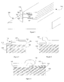
- an optical modulator device 100 known as an electro-absorption modulator is shown.
- the optical modulator device 100 is formed as an integrated circuit or chip having a base 104 formed of a suitable material such as indium phosphide (InP).
- the optical modulator 100 can be a stand alone unit or it can be monolithically integrated, for example, with another device, or, for example, with an integrated passive waveguiding section.
- the base 104 extends into a waveguide 102 through which light either passes or is absorbed.
- the waveguide 102 can be in the form of a ridge as shown in Figure 1, or alternatively, it can be buried in a cladding material.
- the waveguide 102 is any medium, such as a portion of a semiconductor, in which light is confined and through which light can propagate in a directed manner.
- the waveguide 102 consists of layers of different materials forming several regions.
- an active region 106 composed of indium gallium arsenide phosphide (InGaAsP) is followed by a cladding 108 in this case indium phosphide (InP), which is in turn followed by a contact layer 110 such as indium gallium arsenide (InGaAs).
- the contact layer 110 acts as an electrical conductor.
- a metallic stripe which forms an electrode 112 and is in contact with the contact layer 110. This electrode 112 cooperates with a metal contact (not shown) beneath the base of the device 100 to permit a reverse electrical bias to be applied to the device 100.
- the quaternary composition of the active region 106 acts as a band gap for the light. In other words, light passes freely through the waveguide 102.
- the introduction of a reverse electrical bias changes the semiconductor properties of the active region 106 so that there is direct material absorption of light in the waveguide 102. If the reverse electrical bias is sufficiently large, the light will effectively be prevented from passing through the device 100. For example, from a base voltage of 0V during normal operation, applying a bias of -2V can extinguish 99% of the light passing through the device 100.
- the electrode 112 does not extend the entire length of the waveguide 102 and ends before the point of optical entry 120 of the laser light. As previously indicated, the region of electrical contact of the electrode 112 is limited to reduce capacitance and other side effects.
- the electrode 112 of the present device consists of three layers of metal: a gold (Au) layer 122, a platinum (Pt) layer 124 and a titanium (Ti) layer 126.
- Au gold
- Pt platinum
- Ti titanium
- Other combinations of metals are also possible depending on the specific details of the composition of the device 100.
- the intermediate platinum layer 124 is necessary to prevent gold from diffusing into the device 100 through the InGaAs layer 110 which would render the device 100 inoperative. Under conventional techniques, an abrupt termination of the electrode 112 results in a tapering (not shown) of all three layers (122, 124, 126) of the electrode 112.
- one technique for ensuring that gold does not diffuse into the device 100 is to terminate the electrode 112 in a raised fashion away from the device 100. Since the raised terminal end 136 of the electrode 112 does not make contact with the contact layer 110, there is no possibility of gold diffusing into the contact layer 110 from the raised end 136 of the electrode 112. Since the protection of the platinum layer 124 there is unimportant, an abrupt termination of the electrode 112 is acceptable.
- the electrode 112 In addition to functioning as an electrical path, the electrode 112 also acts as a thermal path for heat within the waveguide 102. Heat generated in the waveguide 102 flows through the contact layer 110 into the metallic electrode 112 where it is carried away.
- the electrode 112 is typically connected or extended to a massive bond pad (not shown) to which a wire or other electrical contact (not shown) can be made.
- the electrode 112 also functions to create a thermal path to the relatively massive bond pad which acts as a heat sink for the device 100.
- the electrode 112 is extended beyond the region of desired electrical contact as illustrated in Figure 4.
- the electrically conducting contact layer 110 is replaced by an isolation dielectric 140 such as silicon nitride (SiN) or silicon oxynitride in this region.
- SiN silicon nitride
- the electrode 112 and contact layer 110 provides an electrical path and a thermal path whereas outside the region of desired electrical contact the electrode 112 and SiN layer 114 provide a thermal path but not an electrical path.
- heat is dissipated from the waveguide 102 beyond the region of electrical contact.
- the site of previous failure due to local overheating now has means for dissipating some of the heat.
- the device 100 in accordance with the present invention can handle greater optical power or alternatively, can operate under a greater reverse electrical bias.
- the contact layer 110 and isolation dielectric 140 materials are shown as adjacent and abutting at the juncture or common boundary between the materials.
- a gap is formed between the two layers exposing a portion of the base layer 100.
- a region of overlap 150 of the contact layer 110 and isolation dielectric 140 materials can be formed during the masking process to ensure complete coverage of the base layer 108 at the juncture or common boundary 142.
- the electrode 112 is spaced from the common boundary 142 in an arch which bridges the juncture. This is done to protect the electrode 112 from stress which may occur at that discontinuity.
- An alternative embodiment is illustrated in Figure 6, in which the electrode 112 is suitably modified, for example by increasing its thickness or increasing its strength through annealing, and is in continuous contact with the contact layer 110 and isolation dielectric 140 materials over the common boundary 142. This increases the contact of the electrode 112 with the waveguide 102 and prevents or reduces the possibility of a relative hot spot developing below the common boundary 142. This also facilitates the manufacturing process as the extra effort required for construction of the arch is no longer required.
- FIG. 7 A further embodiment of the present invention is illustrated in Figure 7.
- the isolation dielectric, SiN 140 extends beyond the termination of electrode 112 and the termination is not raised. This technique is particularly appropriate where the isolation dielectric 140 is not susceptible to diffusing undesirable metals. For example, since gold cannot permeate SiN, the previously required raised termination technique is no longer required. Thus, the electrode 112 can be abruptly terminated above and adjacent the SiN isolation dielectric 140.
- a Mach-Zehnder modulator 800 comprises two portions, an attenuation portion 802 and an interferometer portion 804. Light flows into the modulator 800 in the direction indicated.
- the attenuator portion 802 includes a straight portion 806 of the waveguide and a semiconductor device 808, employing technology similar to that discussed above for the electro-absorption modulator, to control the strength of the light source introduced into the rest of the device 800.
- the interferometer portion 804 includes a bifurcated optical path 810 to split the incoming light.
- Each arm is provided with a semiconductor device 812 again using known technology similar to that previously discussed, to alter the physical properties of the waveguide. In essence the index of refraction of each arm is modified so that when the separated streams of light merge into a single stream, they can be controlled to constructively or destructively interfere with each other.
- the use of the present invention to prevent local overheating in the attenuation portion 802 of the Mach-Zehnder modulator 800 is directly analogous to the examples discussed above. It is less necessary in the interferometer portion 804, since the interferometer uses constructive interference and not direct material absorption to modulate light, and there is relatively little heating due to absorption. Nonetheless, accidental absorption can be a problem and the present invention can be applied to decrease the possibility of local overheating in the interferometer portion 804 as well.
- an electrode of a waveguide in a photo detector or semiconductor optical amplifier can be extended beyond the region of desired electrical contact with the waveguide while providing a corresponding non-electrically conducting portion of the contact layer to reduce local overheating in the device.
- a further application of the present invention relates to its use to improve the functioning of lasers such as the 980 nm pump laser.
- lasers such as the 980 nm pump laser.
- overheating of a region of the waveguide in the vicinity of the facet is a problem.
- Extending the electrode of the device beyond the region of desired electrical contact, for example, to an inactive window structure while providing a corresponding non-electrically conducting portion of the contact layer would allow heat to be carried away from the overheated region without making undesired electrical contact with the device.
- the method of the present invention begins by providing a waveguide covered with a conventional contact layer 110 of InGaAs. Referring to Figure 10, this layer 110 is removed by conventional masking and etching techniques in the region outside the region of desired electrical contact. Next, as illustrated in Figure 11, a blanket deposition of isolation dielectric 140 is made. Next, as illustrated in Figure 12, a further masking and etching step removes the isolation dielectric 140 from the region of desired electrical contact. An overlap 150 between the two regions can be created as illustrated in Figure 12, or the two regions can be flush as illustrated in Figure 4, depending on the masking procedure chosen. Finally, the electrode 112 is deposited on the covered waveguide 102 as illustrated in Figure 13.
- a suitable material such as PMGI (poly(dimethyl glutarimide)
- PMGI poly(dimethyl glutarimide)
- PMGI poly(dimethyl glutarimide)
- PMGI is a deep UV sensitive material which can be applied and then heated to a plastic state. Because of reflow during heating, it forms a rounded boss 160.
- the electrode layers are then deposited over the PMGI boss 160 to form the desired arched electrode 112. Finally, the PMGI boss 160 can be dissolved and washed away.
Landscapes
- Physics & Mathematics (AREA)
- Nonlinear Science (AREA)
- General Physics & Mathematics (AREA)
- Optics & Photonics (AREA)
- Optical Modulation, Optical Deflection, Nonlinear Optics, Optical Demodulation, Optical Logic Elements (AREA)
- Optical Integrated Circuits (AREA)
Applications Claiming Priority (2)
| Application Number | Priority Date | Filing Date | Title |
|---|---|---|---|
| US709646 | 2000-11-13 | ||
| US09/709,646 US6654534B1 (en) | 2000-11-13 | 2000-11-13 | Electrode, termination for reduced local heating in an optical device |
Publications (3)
| Publication Number | Publication Date |
|---|---|
| EP1205785A2 true EP1205785A2 (de) | 2002-05-15 |
| EP1205785A3 EP1205785A3 (de) | 2003-03-12 |
| EP1205785B1 EP1205785B1 (de) | 2005-01-12 |
Family
ID=24850755
Family Applications (1)
| Application Number | Title | Priority Date | Filing Date |
|---|---|---|---|
| EP01309541A Expired - Lifetime EP1205785B1 (de) | 2000-11-13 | 2001-11-12 | Elektrodenabschluss zur Reduzierung von lokaler Erhitzung in einer optischen Vorrichtung |
Country Status (4)
| Country | Link |
|---|---|
| US (1) | US6654534B1 (de) |
| EP (1) | EP1205785B1 (de) |
| CA (1) | CA2361683A1 (de) |
| DE (1) | DE60108336T2 (de) |
Cited By (1)
| Publication number | Priority date | Publication date | Assignee | Title |
|---|---|---|---|---|
| CN112019250A (zh) * | 2020-10-29 | 2020-12-01 | 三维通信股份有限公司 | 过温功率自动调整方法和装置、存储介质 |
Families Citing this family (10)
| Publication number | Priority date | Publication date | Assignee | Title |
|---|---|---|---|---|
| US7715732B2 (en) * | 2004-08-05 | 2010-05-11 | Jds Uniphase Corporation | Bias-control for optical Mach-Zehnder modulators with voltage-induced optical absorption |
| GB2446611B (en) * | 2007-02-14 | 2011-08-17 | Bookham Technology Plc | Low creep metallization for optoelectronic applications |
| CN102723383B (zh) * | 2012-06-19 | 2016-01-06 | 电子科技大学 | 用于垂直方向耦合的光电探测器的光波导结构 |
| CN104426613B (zh) * | 2013-08-19 | 2017-09-19 | 上海贝尔股份有限公司 | 用于光接入网络的突发模式接收机及其使用和制造方法 |
| US9588360B2 (en) | 2014-03-31 | 2017-03-07 | Mellanox Technologies Silicon Photonics Inc. | Temperature control of components on an optical device |
| CN105842799B (zh) * | 2016-05-25 | 2018-01-16 | 电子科技大学 | 大横截面单模方向耦合光波导探测器 |
| US10852478B1 (en) | 2019-05-28 | 2020-12-01 | Ciena Corporation | Monolithically integrated gain element |
| US12470045B2 (en) | 2019-05-28 | 2025-11-11 | Ciena Corporation | Semiconductor device with selective area epitaxy growth utilizing a mask to suppress or enhance growth at the edges |
| JP7404711B2 (ja) * | 2019-08-23 | 2023-12-26 | 住友電気工業株式会社 | 光変調器 |
| CN115548878B (zh) * | 2021-06-29 | 2025-10-17 | 青岛联智光通信技术有限公司 | 一种具有调制器的激光芯片、准备方法及光模块 |
Family Cites Families (18)
| Publication number | Priority date | Publication date | Assignee | Title |
|---|---|---|---|---|
| WO1990003055A1 (fr) * | 1988-09-01 | 1990-03-22 | Seiko Epson Corporation | Dispositif photo-emetteur et procede de production |
| US5098178A (en) * | 1989-05-30 | 1992-03-24 | Ugur Ortabasi | Superconducting matrix |
| EP0410067B1 (de) * | 1989-07-27 | 1993-09-22 | International Business Machines Corporation | Integrierte Halbleiterdiodenlaser und Photodiodenstruktur |
| JPH04209576A (ja) * | 1990-12-07 | 1992-07-30 | Kanegafuchi Chem Ind Co Ltd | 光電変換素子 |
| FR2672398B1 (fr) * | 1991-02-01 | 1993-11-19 | Alcatel Nv | Dispositif electro-optique a guide d'onde. |
| US5345108A (en) * | 1991-02-26 | 1994-09-06 | Nec Corporation | Semiconductor device having multi-layer electrode wiring |
| JP3025982B2 (ja) * | 1992-01-21 | 2000-03-27 | イビデン株式会社 | 導波路型光方向性結合器 |
| DE4237519C1 (de) * | 1992-11-06 | 1994-03-31 | Dornier Gmbh | Festelektrolyt mit darauf angebrachter mehrschichtiger Elektrode |
| JPH0720506A (ja) * | 1993-06-30 | 1995-01-24 | Mitsubishi Electric Corp | 光スイッチ及びその製造方法 |
| JP3117107B2 (ja) * | 1993-08-03 | 2000-12-11 | シャープ株式会社 | 光集積回路素子の組立構造 |
| KR0179677B1 (ko) * | 1993-12-28 | 1999-04-15 | 사토 후미오 | 반도체장치 및 그 제조방법 |
| JP2894961B2 (ja) * | 1994-11-18 | 1999-05-24 | 日本電気株式会社 | 光制御デバイス |
| US5889913A (en) * | 1995-03-15 | 1999-03-30 | Kabushiki Kaisha Toshiba | Optical semiconductor device and method of fabricating the same |
| JPH08288541A (ja) * | 1995-04-20 | 1996-11-01 | Hitachi Ltd | 半導体光集積化素子、及び光ジャイロ |
| JPH0964399A (ja) * | 1995-08-29 | 1997-03-07 | Furukawa Electric Co Ltd:The | 導波路型受光素子 |
| US6044098A (en) * | 1997-08-29 | 2000-03-28 | Xerox Corporation | Deep native oxide confined ridge waveguide semiconductor lasers |
| US6198853B1 (en) * | 1997-10-31 | 2001-03-06 | Oki Electric Industry Co., Ltd. | Semiconductor optical functional element |
| JP3662402B2 (ja) * | 1997-11-07 | 2005-06-22 | 三菱電機株式会社 | 光半導体モジュール |
-
2000
- 2000-11-13 US US09/709,646 patent/US6654534B1/en not_active Expired - Lifetime
-
2001
- 2001-11-09 CA CA002361683A patent/CA2361683A1/en not_active Abandoned
- 2001-11-12 EP EP01309541A patent/EP1205785B1/de not_active Expired - Lifetime
- 2001-11-12 DE DE60108336T patent/DE60108336T2/de not_active Expired - Lifetime
Cited By (1)
| Publication number | Priority date | Publication date | Assignee | Title |
|---|---|---|---|---|
| CN112019250A (zh) * | 2020-10-29 | 2020-12-01 | 三维通信股份有限公司 | 过温功率自动调整方法和装置、存储介质 |
Also Published As
| Publication number | Publication date |
|---|---|
| EP1205785A3 (de) | 2003-03-12 |
| US6654534B1 (en) | 2003-11-25 |
| DE60108336D1 (de) | 2005-02-17 |
| CA2361683A1 (en) | 2002-05-13 |
| DE60108336T2 (de) | 2006-03-02 |
| EP1205785B1 (de) | 2005-01-12 |
Similar Documents
| Publication | Publication Date | Title |
|---|---|---|
| EP1205785B1 (de) | Elektrodenabschluss zur Reduzierung von lokaler Erhitzung in einer optischen Vorrichtung | |
| JP4828018B2 (ja) | 光変調器およびその製造方法並びに光半導体装置 | |
| US10031355B2 (en) | Temperature control of components on an optical device | |
| CN106575852B (zh) | 光学装置上的部件的温度控制 | |
| JP2004053830A (ja) | 光半導体装置 | |
| US20240170914A1 (en) | Semiconductor sub-assemblies for emitting modulated light | |
| US6191464B1 (en) | Electrical isolation of opto-electronic device components | |
| US20180031764A1 (en) | Semiconductor optical apparatus | |
| US20140294335A1 (en) | Method for manufacturing semiconductor modulator and semiconductor modulator | |
| CN114114721A (zh) | 光调制器 | |
| US11837620B2 (en) | Photo receiver | |
| CN115428280B (zh) | 半导体光集成元件 | |
| JP4147858B2 (ja) | 光デバイスおよびその製造方法 | |
| JP4075367B2 (ja) | 半導体素子およびその製造方法 | |
| JP2010237296A (ja) | 光半導体装置 | |
| JP3254053B2 (ja) | 光集積回路 | |
| JP2010230978A (ja) | 光半導体装置及びその製造方法 | |
| JP3717639B2 (ja) | 光変調器モジュール | |
| JP2760276B2 (ja) | 選択成長導波型光制御素子 | |
| US20260063964A1 (en) | Optical modulator | |
| JP3966412B2 (ja) | 半導体光素子 | |
| JP2011175216A (ja) | 半導体光素子、半導体マッハツェンダー型光変調器および半導体光素子の製造方法 | |
| JP7813155B2 (ja) | 半導体光素子 | |
| JP2026056862A (ja) | 光変調器 | |
| CN112666653A (zh) | 光调制器 |
Legal Events
| Date | Code | Title | Description |
|---|---|---|---|
| PUAI | Public reference made under article 153(3) epc to a published international application that has entered the european phase |
Free format text: ORIGINAL CODE: 0009012 |
|
| AK | Designated contracting states |
Kind code of ref document: A2 Designated state(s): AT BE CH CY DE DK ES FI FR GB GR IE IT LI LU MC NL PT SE TR |
|
| AX | Request for extension of the european patent |
Free format text: AL;LT;LV;MK;RO;SI |
|
| PUAL | Search report despatched |
Free format text: ORIGINAL CODE: 0009013 |
|
| AK | Designated contracting states |
Kind code of ref document: A3 Designated state(s): AT BE CH CY DE DK ES FI FR GB GR IE IT LI LU MC NL PT SE TR Designated state(s): AT BE CH CY DE DK ES FI FR GB GR IE IT LI LU MC NL PT SE TR |
|
| AX | Request for extension of the european patent |
Extension state: AL LT LV MK RO SI |
|
| RIC1 | Information provided on ipc code assigned before grant |
Ipc: 7G 02F 1/015 B Ipc: 7H 01S 3/04 B Ipc: 7G 02F 1/035 A |
|
| RAP1 | Party data changed (applicant data changed or rights of an application transferred) |
Owner name: BOOKHAM TECHNOLOGY PLC |
|
| 17P | Request for examination filed |
Effective date: 20030902 |
|
| AKX | Designation fees paid |
Designated state(s): DE FR GB |
|
| GRAP | Despatch of communication of intention to grant a patent |
Free format text: ORIGINAL CODE: EPIDOSNIGR1 |
|
| GRAS | Grant fee paid |
Free format text: ORIGINAL CODE: EPIDOSNIGR3 |
|
| 111Z | Information provided on other rights and legal means of execution |
Free format text: DEFRGB Effective date: 20031030 |
|
| GRAA | (expected) grant |
Free format text: ORIGINAL CODE: 0009210 |
|
| AK | Designated contracting states |
Kind code of ref document: B1 Designated state(s): DE FR GB |
|
| REG | Reference to a national code |
Ref country code: GB Ref legal event code: FG4D |
|
| REF | Corresponds to: |
Ref document number: 60108336 Country of ref document: DE Date of ref document: 20050217 Kind code of ref document: P |
|
| REG | Reference to a national code |
Ref country code: IE Ref legal event code: FG4D |
|
| PLBE | No opposition filed within time limit |
Free format text: ORIGINAL CODE: 0009261 |
|
| STAA | Information on the status of an ep patent application or granted ep patent |
Free format text: STATUS: NO OPPOSITION FILED WITHIN TIME LIMIT |
|
| ET | Fr: translation filed | ||
| 26N | No opposition filed |
Effective date: 20051013 |
|
| REG | Reference to a national code |
Ref country code: GB Ref legal event code: 732E |
|
| REG | Reference to a national code |
Ref country code: GB Ref legal event code: 732E Free format text: REGISTERED BETWEEN 20140612 AND 20140618 |
|
| REG | Reference to a national code |
Ref country code: DE Ref legal event code: R082 Ref document number: 60108336 Country of ref document: DE Representative=s name: PATENTANWAELTE WALLACH, KOCH & PARTNER, DE |
|
| REG | Reference to a national code |
Ref country code: DE Ref legal event code: R082 Ref document number: 60108336 Country of ref document: DE Representative=s name: PATENTANWAELTE WALLACH, KOCH & PARTNER, DE Effective date: 20150422 Ref country code: DE Ref legal event code: R081 Ref document number: 60108336 Country of ref document: DE Owner name: OCLARO TECHNOLOGY LIMITED, TOWCESTER, GB Free format text: FORMER OWNER: BOOKHAM TECHNOLOGY PLC, ABINGDON, OXFORDSHIRE, GB Effective date: 20150422 Ref country code: DE Ref legal event code: R082 Ref document number: 60108336 Country of ref document: DE Representative=s name: PATENTANWAELTE WALLACH, KOCH, DR. HAIBACH, FEL, DE Effective date: 20150422 |
|
| REG | Reference to a national code |
Ref country code: FR Ref legal event code: PLFP Year of fee payment: 15 |
|
| REG | Reference to a national code |
Ref country code: FR Ref legal event code: PLFP Year of fee payment: 16 |
|
| REG | Reference to a national code |
Ref country code: FR Ref legal event code: PLFP Year of fee payment: 17 |
|
| REG | Reference to a national code |
Ref country code: FR Ref legal event code: PLFP Year of fee payment: 18 |
|
| PGFP | Annual fee paid to national office [announced via postgrant information from national office to epo] |
Ref country code: DE Payment date: 20201125 Year of fee payment: 20 Ref country code: GB Payment date: 20201127 Year of fee payment: 20 Ref country code: FR Payment date: 20201126 Year of fee payment: 20 |
|
| REG | Reference to a national code |
Ref country code: DE Ref legal event code: R071 Ref document number: 60108336 Country of ref document: DE |
|
| REG | Reference to a national code |
Ref country code: GB Ref legal event code: PE20 Expiry date: 20211111 |
|
| PG25 | Lapsed in a contracting state [announced via postgrant information from national office to epo] |
Ref country code: GB Free format text: LAPSE BECAUSE OF EXPIRATION OF PROTECTION Effective date: 20211111 |