EP1207048A1 - Verfahren und Vorrichtung zur Bildaufzeichnung von Mustern auf Filmen durch die Verwendung von Temperaturgradienten - Google Patents
Verfahren und Vorrichtung zur Bildaufzeichnung von Mustern auf Filmen durch die Verwendung von Temperaturgradienten Download PDFInfo
- Publication number
- EP1207048A1 EP1207048A1 EP00124205A EP00124205A EP1207048A1 EP 1207048 A1 EP1207048 A1 EP 1207048A1 EP 00124205 A EP00124205 A EP 00124205A EP 00124205 A EP00124205 A EP 00124205A EP 1207048 A1 EP1207048 A1 EP 1207048A1
- Authority
- EP
- European Patent Office
- Prior art keywords
- film
- temperature gradient
- substrate
- substrate surface
- anyone
- Prior art date
- Legal status (The legal status is an assumption and is not a legal conclusion. Google has not performed a legal analysis and makes no representation as to the accuracy of the status listed.)
- Withdrawn
Links
- 238000000034 method Methods 0.000 title claims abstract description 41
- 230000008569 process Effects 0.000 title abstract description 24
- 230000015572 biosynthetic process Effects 0.000 title description 2
- 239000000758 substrate Substances 0.000 claims abstract description 104
- 238000012546 transfer Methods 0.000 claims abstract description 4
- 239000010410 layer Substances 0.000 claims description 26
- XUIMIQQOPSSXEZ-UHFFFAOYSA-N Silicon Chemical compound [Si] XUIMIQQOPSSXEZ-UHFFFAOYSA-N 0.000 claims description 9
- 229910052710 silicon Inorganic materials 0.000 claims description 9
- 239000010703 silicon Substances 0.000 claims description 9
- 238000000151 deposition Methods 0.000 claims description 7
- 229920000620 organic polymer Polymers 0.000 claims description 7
- 239000004065 semiconductor Substances 0.000 claims description 4
- 239000002356 single layer Substances 0.000 claims description 4
- 239000004020 conductor Substances 0.000 claims description 3
- 239000004793 Polystyrene Substances 0.000 description 18
- 229920002223 polystyrene Polymers 0.000 description 14
- 230000005855 radiation Effects 0.000 description 14
- 239000000463 material Substances 0.000 description 13
- 239000007788 liquid Substances 0.000 description 10
- 229920000642 polymer Polymers 0.000 description 10
- 229920006254 polymer film Polymers 0.000 description 8
- PCHJSUWPFVWCPO-UHFFFAOYSA-N gold Chemical compound [Au] PCHJSUWPFVWCPO-UHFFFAOYSA-N 0.000 description 7
- 239000010931 gold Substances 0.000 description 7
- 229910052737 gold Inorganic materials 0.000 description 7
- 239000011343 solid material Substances 0.000 description 7
- 230000003287 optical effect Effects 0.000 description 5
- 230000008021 deposition Effects 0.000 description 4
- 230000004907 flux Effects 0.000 description 4
- 238000000879 optical micrograph Methods 0.000 description 4
- 239000007787 solid Substances 0.000 description 4
- 239000000126 substance Substances 0.000 description 4
- 230000000930 thermomechanical effect Effects 0.000 description 4
- 230000003321 amplification Effects 0.000 description 3
- 238000001816 cooling Methods 0.000 description 3
- 238000005530 etching Methods 0.000 description 3
- 238000010438 heat treatment Methods 0.000 description 3
- 239000011344 liquid material Substances 0.000 description 3
- 238000003199 nucleic acid amplification method Methods 0.000 description 3
- 238000000206 photolithography Methods 0.000 description 3
- 229920003229 poly(methyl methacrylate) Polymers 0.000 description 3
- 239000004926 polymethyl methacrylate Substances 0.000 description 3
- 238000004458 analytical method Methods 0.000 description 2
- 238000000137 annealing Methods 0.000 description 2
- 238000000089 atomic force micrograph Methods 0.000 description 2
- 238000004630 atomic force microscopy Methods 0.000 description 2
- 230000003247 decreasing effect Effects 0.000 description 2
- 230000000694 effects Effects 0.000 description 2
- 238000002474 experimental method Methods 0.000 description 2
- 230000009477 glass transition Effects 0.000 description 2
- 238000000059 patterning Methods 0.000 description 2
- 229920002120 photoresistant polymer Polymers 0.000 description 2
- 230000001902 propagating effect Effects 0.000 description 2
- 230000010076 replication Effects 0.000 description 2
- 230000004044 response Effects 0.000 description 2
- 239000002904 solvent Substances 0.000 description 2
- RYGMFSIKBFXOCR-UHFFFAOYSA-N Copper Chemical compound [Cu] RYGMFSIKBFXOCR-UHFFFAOYSA-N 0.000 description 1
- 150000001335 aliphatic alkanes Chemical class 0.000 description 1
- 229910045601 alloy Inorganic materials 0.000 description 1
- 239000000956 alloy Substances 0.000 description 1
- 238000013459 approach Methods 0.000 description 1
- 238000003491 array Methods 0.000 description 1
- 238000003486 chemical etching Methods 0.000 description 1
- 238000006243 chemical reaction Methods 0.000 description 1
- 229910052802 copper Inorganic materials 0.000 description 1
- 239000010949 copper Substances 0.000 description 1
- 238000004132 cross linking Methods 0.000 description 1
- 238000013461 design Methods 0.000 description 1
- 230000000368 destabilizing effect Effects 0.000 description 1
- 239000006185 dispersion Substances 0.000 description 1
- 238000006073 displacement reaction Methods 0.000 description 1
- 238000009826 distribution Methods 0.000 description 1
- 238000010894 electron beam technology Methods 0.000 description 1
- 230000005284 excitation Effects 0.000 description 1
- 238000011049 filling Methods 0.000 description 1
- 238000002844 melting Methods 0.000 description 1
- 230000008018 melting Effects 0.000 description 1
- 239000002184 metal Substances 0.000 description 1
- 229910052751 metal Inorganic materials 0.000 description 1
- 150000002739 metals Chemical class 0.000 description 1
- 238000000813 microcontact printing Methods 0.000 description 1
- 238000004377 microelectronic Methods 0.000 description 1
- 238000000399 optical microscopy Methods 0.000 description 1
- 238000001020 plasma etching Methods 0.000 description 1
- 229920000058 polyacrylate Polymers 0.000 description 1
- 229920000307 polymer substrate Polymers 0.000 description 1
- 238000006116 polymerization reaction Methods 0.000 description 1
- 229920000193 polymethacrylate Polymers 0.000 description 1
- 239000010970 precious metal Substances 0.000 description 1
- 238000002360 preparation method Methods 0.000 description 1
- 238000010791 quenching Methods 0.000 description 1
- 230000000171 quenching effect Effects 0.000 description 1
- 230000000717 retained effect Effects 0.000 description 1
- 229920006126 semicrystalline polymer Polymers 0.000 description 1
- 238000000926 separation method Methods 0.000 description 1
- 238000003980 solgel method Methods 0.000 description 1
- 125000006850 spacer group Chemical group 0.000 description 1
- 238000004528 spin coating Methods 0.000 description 1
- 238000005507 spraying Methods 0.000 description 1
- 230000002123 temporal effect Effects 0.000 description 1
- 238000012876 topography Methods 0.000 description 1
Images




Classifications
-
- B—PERFORMING OPERATIONS; TRANSPORTING
- B41—PRINTING; LINING MACHINES; TYPEWRITERS; STAMPS
- B41C—PROCESSES FOR THE MANUFACTURE OR REPRODUCTION OF PRINTING SURFACES
- B41C1/00—Forme preparation
- B41C1/10—Forme preparation for lithographic printing; Master sheets for transferring a lithographic image to the forme
- B41C1/1041—Forme preparation for lithographic printing; Master sheets for transferring a lithographic image to the forme by modification of the lithographic properties without removal or addition of material, e.g. by the mere generation of a lithographic pattern
-
- B—PERFORMING OPERATIONS; TRANSPORTING
- B41—PRINTING; LINING MACHINES; TYPEWRITERS; STAMPS
- B41M—PRINTING, DUPLICATING, MARKING, OR COPYING PROCESSES; COLOUR PRINTING
- B41M5/00—Duplicating or marking methods; Sheet materials for use therein
- B41M5/26—Thermography ; Marking by high energetic means, e.g. laser otherwise than by burning, and characterised by the material used
-
- B—PERFORMING OPERATIONS; TRANSPORTING
- B41—PRINTING; LINING MACHINES; TYPEWRITERS; STAMPS
- B41M—PRINTING, DUPLICATING, MARKING, OR COPYING PROCESSES; COLOUR PRINTING
- B41M5/00—Duplicating or marking methods; Sheet materials for use therein
- B41M5/26—Thermography ; Marking by high energetic means, e.g. laser otherwise than by burning, and characterised by the material used
- B41M5/36—Thermography ; Marking by high energetic means, e.g. laser otherwise than by burning, and characterised by the material used using a polymeric layer, which may be particulate and which is deformed or structurally changed with modification of its' properties, e.g. of its' optical hydrophobic-hydrophilic, solubility or permeability properties
-
- B—PERFORMING OPERATIONS; TRANSPORTING
- B82—NANOTECHNOLOGY
- B82Y—SPECIFIC USES OR APPLICATIONS OF NANOSTRUCTURES; MEASUREMENT OR ANALYSIS OF NANOSTRUCTURES; MANUFACTURE OR TREATMENT OF NANOSTRUCTURES
- B82Y30/00—Nanotechnology for materials or surface science, e.g. nanocomposites
-
- G—PHYSICS
- G05—CONTROLLING; REGULATING
- G05D—SYSTEMS FOR CONTROLLING OR REGULATING NON-ELECTRIC VARIABLES
- G05D23/00—Control of temperature
- G05D23/19—Control of temperature characterised by the use of electric means
- G05D23/1927—Control of temperature characterised by the use of electric means using a plurality of sensors
- G05D23/193—Control of temperature characterised by the use of electric means using a plurality of sensors sensing the temperaure in different places in thermal relationship with one or more spaces
- G05D23/1935—Control of temperature characterised by the use of electric means using a plurality of sensors sensing the temperaure in different places in thermal relationship with one or more spaces using sequential control
Definitions
- the present invention relates to a process and an apparatus for producing patterns, particularly high-resolution patterns, in films which are exposed to temperature gradients.
- a process for producing lithographic structures by exposing at least one film on a substrate to a temperature gradient, the temperature gradient generating forces in the film which cause a mass transfer in the film to thereby produce a lithographic pattern.
- photolithography is used to produce patterns on substrates.
- Photolithography techniques involve exposing a photoresist to an optical pattern and using chemicals to etch either the exposed or unexposed portions of the photoresist to produce the pattern on the substrate.
- the resolution of the pattern is thus limited by the wavelength of light used to produce the optical pattern. Since smaller wavelengths have to be used to produce sub-micron patterns, photolithography becomes increasingly complex and costly.
- the process according to the present invention includes several advantages. For example patterns are produced without optical radiation. In principle, the lateral resolution of the pattern can be made arbitrarily small by controlling the applied temperature gradient and selecting a film with appropriate properties. Furthermore, high-resolution patterns, e.g. lithographic structures, can be obtained by the process according to the present invention without requiring the use of chemicals to etch or remove portions of the film.
- the temperature gradient to which the at least one film is exposed is preferably within the range of 10 6 °C/m to 10 10 °C/m, more preferably 10 7 °C/m to 10 9 °C/m.
- the film can be present in a liquid or a solid state.
- the deposition of the at least one film in step (b) can be carried out by the conventionally known techniques like spin coating, spraying, immersing, etc..
- the film is liquid after its deposition onto the substrate surface. If the film is not liquid after its deposition onto the substrate surface, the film can be liquefied before and/or during exposition to a temperature gradient in step (c) of the process according to the present invention.
- the liquefaction can be performed by e.g.
- the film can then be solidified, for example, by cooling, a chemical reaction, a cross-linking process, a polymerization reaction, or by using a sol-gel process.
- the film to be patterned can be of a single layer or can include a plurality of layers, i.e. two or more iterations.
- the thermally conducting material which is contained in the at least one film to be patterned is preferably an organic polymer or an organic oligomer.
- the molecular weight of the organic polymer or organic oligomer used is not subject to any particular limitation. For example, polymers having a molecular weight of approximately 100 g/mol can be used.
- the organic polymer usable in course of the process according to the present invention polystyrene, partially or fully chlorinated or brominated polystyrene, polyacrylates and polymethacrylates can be exemplified.
- step (c) of the process according to the present invention it is particularly preferred to keep the film during the operation of step (c) of the process according to the present invention above the glass transition temperature of the organic polymer used.
- the substrate can include a single layer or a plurality of layers.
- the substrate surface can be a surface of a solid or liquid material.
- the substrate can be a semiconductor wafer, more preferably a silicon wafer.
- Such a semiconductor wafer can also be coated with a precious metal layer like e.g. a gold layer in order to increase the acoustic impedance difference at the film-substrate interface.
- the film thickness is within the range of 10 nm to 1000 nm, more preferably 50 nm to 250 nm.
- the temperature gradient is generated by bringing the substrate surface and a mounting surface provided opposite to the substrate surface into thermal contact with first and second temperature control means set at different temperatures.
- the spacing between the substrate surface and the mounting surface is preferably within the range of 10 nm to 5000 nm, more preferably 50 nm to 1000 nm, even more preferably 150 nm to 600 nm.
- the pattern obtained by the process according to the present invention can be further specified by spatially controlling the temperature gradient.
- the pattern can be even further specified by spatially varying the surface energy of one of the substrate surface and the mounting surface.
- the process according to the present invention can form a patterned film with lateral features smaller than 10 ⁇ m, particularly smaller than 1 ⁇ m, more particularly smaller than 100 nm.
- the resolution of the pattern depends on the magnitude of the temperature gradient, the thickness of the film, the surface tension of the film material, the difference of the velocity of sound of the film material and the substrate, the thermal conductivities of the film material and the adjacent medium and the difference in density between the film material and the adjacent medium such as for example air.
- the velocity of sound (at an acoustic wavelength of approximately 1 ⁇ m) of polystyrene is 1250 m/s, of polymethylmethacrylate 2150 m/s and of silicon used as substrate 8400 m/s, respectively;
- the thermal conductivity of polystyrene is 0.16 W/mK, of polymethylmethacrylate 0.20 W/mK and of air 0.034 W/mK;
- the density of polystyrene is 0.987 g/m 3 , of polymethylmethacrylate 1.116 g/m 3 and of silicon used as substrate is 2.33 g/m 3 ; and the surface tension of polystyrene is 0.03 N/m.
- the pattern on the film can be transferred to another substrate using conventionally known etching techniques, e.g. reactive ion or chemical etching procedures.
- the patterned film itself can be used in subsequent applications, such as in a device, e.g. a diode, a transistor, a display device, or a chemical, biological, medical or mechanical sensor or part thereof.
- an apparatus for producing a patterned film comprising a substrate having a substrate surface for supporting the film to be patterned; a temperature gradient generator for generating a temperature gradient in a temperature gradient volume, the temperature gradient having a component orientated along a normal direction of the substrate surface, wherein the temperature gradient volume includes at least a volume portion extending from at least an area of the substrate surface in the normal direction thereof.
- the temperature gradient generator comprises at least first and second temperature control means, the temperature control means being spaced apart from each other, so that the substrate is operationally disposed at least partly therebetween and the temperature gradient volume is defined at least partly therebetween.
- a mounting surface is provided opposite to the substrate surface, the first temperature control means being connected to the substrate, while the second temperature control means being connected to the mounting surface. The spacing between the substrate surface and the mounting surface can preferably be within the range of 10 nm to 5000 nm, more preferably 50 nm to 1000 nm, even more preferably 150 nm to 600 nm.
- the temperature control means can be controlled to generate a temperature gradient between the substrate surface and the mounting surface opposite to the substrate surface within the range of 10 6 °C/m to 10 10 °C/m, more preferably 10 7 °C/m to 10 9 °C/m.
- the mounting surface provided opposite to the substrate surface can be, for example, designed in form of a plate (top plate).
- the temperature gradient generator can be adapted to generate at least partly homogenous and/or at least partly heterogeneous temperature gradients, in particular temperature gradients varying laterally over the substrate surface.
- At least one of the substrate surface and/or the mounting surface is patterned with topographic features and/or has a spatially varying surface energy and/or a spatially varying thermal conductivity.
- the film to be patterned and the mounting surface provided opposite thereto can be separated by e.g. an air gap, i.e. the spacing between the substrate surface and the mounting surface can be filled with e.g. air.
- the film and the mounting surface can be separated by any gaseous, liquid or solid material.
- a double layer system of two solid materials can be used, one of the layers acting as the film to be patterned while the upper one superposed thereon serving as adjacent medium. When heated, both of the layers become liquid, while both of the layers, in turn, become solid, when cooled down. As a result, a structure or pattern, respectively, of one material in the other material is obtained.
- the first layer acting as the film to be patterned can be deposited onto the substrate surface and then on the film surface in that order.
- the first layer of the double layer system acting as the film to be patterned can be sandwiched between both gold layers and this assembly can then be applied on the substrate surface, before applying the second layer of the double layer system on the upper gold layer of said assembly.
- the second layer of the double layer system can be applied on said assembly, before applying said assembly on the substrate surface.
- a process using a double layer system is of interest for applications like the semiconductor industry, photo-voltaic applications or for the preparation of photodiodes.
- one of the two solid material can also be removed by e.g. etching or dissolving to obtain a lithographic mask.
- the separation distance i.e. the spacing
- the temperature gradient can be obtained by setting the substrate surface and the mounting surface at two different temperatures controlled by the first and second temperature means.
- the temperatures control means can be, for example, temperature baths, heating devices or cooling devices or other conventional temperature devices known in the art.
- at least one of the substrate surface and/or the mounting surface can be exposed of radiation from a radiation source, i.e. radiation from a radiation source heats the back side of at least one of the substrate surface and/or the mounting surface.
- the radiation source can be, for example, a laser, an infrared lamp, or any other intensive radiation source.
- the radiation source can be operated in a constant mode, i.e.
- the radiation source is switched on for a longer time period of the patterning process, so that a thermal equilibrium, i.e. a contant temperature gradient, is reached. Otherwise, the radiation source can be operated in a pulsed mode, so that a temperature gradient is set up only for a short time to reach, for example, a temperature difference between the substrate surface and the mounting surface, of 1000°C or more, thereby immediately destabilizing the film to be patterned.
- a temperature gradient is set up only for a short time to reach, for example, a temperature difference between the substrate surface and the mounting surface, of 1000°C or more, thereby immediately destabilizing the film to be patterned.
- the latter procedure is particularly advantageous when using film materials having a high melting point such as, for example, metals and alloys.
- the apparatus according to the present invention can be heated or cooled during operation.
- FIG. 1a A preferred embodiment of the apparatus for producing the patterned films according to the present invention is shown in Fig. 1a.
- a film is formed on a substrate, opposed by a mounting surface in form of a plate (top plate).
- the film is a polymer film, but, alternatively, the film can be any liquid or solid material.
- the substrate and the mounting surface are brought into thermal contact with first and second temperature control means which during operation produce a temperature gradient between the substrate surface and the mounting surface designed in form of a top plate.
- a particular medium is present between the film and the mounting surface, which has a thermal conductivity, density or velocity of sound that is different from the film material.
- this medium can be vacuum, air, or any other liquid or solid material.
- the temperature gradient causes the film to form a pattern.
- the film can contain an organic polymer or an organic oligomer.
- the film can contain a glassy polymer (e.g. polystyrene), which has been spin-coated onto the substrate.
- the film is liquefied before and/or during subjecting to the temperature gradient.
- the film when the film is a glassy or semi-crystalline polymer, it may be solid at room temperature and turn liquid upon heating.
- the resulting temperature gradient between the substrate surface and the mounting surface will induce a thermomechanical pressure at the interface between the film and the spacing between the substrate surface and the mounting surface, which will ultimately destabilize the film and dominate over competing forces.
- the film develops a surface undulation with a well-defined wavelength as shown in Fig. 2a. With time, the amplitudes of these waves increase until the film touches the mounting surface (top plate) as shown in Fig. 2b, thereby producing a columnar structure having well-defined column diameters and inter-column spacings.
- solidifying the film material e.g. by cooling, the structure is preserved as shown in Fig. 2c.
- the column diameters and spacings depend on parameters like the temperature difference, the thickness of the film, the thermal conductivities of the film material and the adjacent medium, the densities of the film material and the adjacent medium, and the velocity of sound of the film material and the substrate material.
- thermomechanically induced instability of the film is additionally modified by the lateral temperature gradients.
- This effect can be used to replicate a master pattern to a lateral structure in the film.
- the substrate surface, the mounting surface or both can feature a lateral pattern, i.e. the substrate surface can also be patterned, either in the alternative, or in addition, to the mounting surface.
- Such patterns can be produced, for example, by electron beam etching.
- Fig. 3a wherein the mounting surface is replaced with a top plate which is topographically patterned.
- the externally applied temperature difference causes the film undulations to focus in the direction of the strongest temperature gradient.
- the film forms a pattern corresponding to the topographically patterned top plate, as shown in Fig. 3b.
- the structure in the film is retained, as shown in Fig. 3c.
- the aspect ratio of the patterned film can be significantly greater than that of the patterned plate.
- the spacing between the mounting surface and the substrate surface can be increased, while the film is liquefied and the temperature difference is applied. If necessary, the applied temperatures can be varied during the relative displacement of the mounting surface and the substrate surface.
- the substrate is replaced with a substrate which has a lateral variation in its surface energy.
- the lateral variation in the surface energy can be produced, for example, by micro-contact printing.
- a film is deposited onto the substrate.
- the film can be liquefied and a temperature difference is then applied to the substrate and the top plate.
- the temperature gradient results in an instability of the film as described above.
- the developing surface undulations align with respect to the surface energy pattern of the substrate.
- the structure in the film thus obtained is then preserved by solidifying the polymer.
- the mounting surface can have a lateral variation in surface energy, either in the alternative, or in addition, to the substrate surface.
- the thermal conductivities of either the substrate surface and/or the mounting surface can spatially vary.
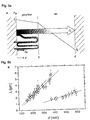
- the origin of the film instability can be understood when considering the balance of forces which act at a polymer-air-interface (cf. Fig. 5a).
- the surface tension ⁇ minimizes the polymer-air- surface area and stabilizes the homogeneous polymer film.
- the temperature gradient causes a flux of thermal energy J q in the polymer film and the air gap. Associated with the flow J q is a flux of thermal excitations, so-called phonons ( J ph ), towards lower temperatures as shown in Fig. 5a. Due to the different acoustic impedances of the two layers, the phonons propagating in the polymer film are nearly perfectly reflected at the liquid-air interface.
- the reflections of the phonons at the film surface gives rise to a radiation pressure.
- This radiation pressure is additionally amplified by multiple reflections at the film-air and film-substrate interfaces.
- the radiation pressure p r is opposed by the Laplace pressure which stems from the surface tension.
- a local perturbation in the film thickness h results in a pressure gradient which drives a flow of the liquid in the plane of the film.
- the liquid flow next to a solid surface is given by a Poiseuille type formula, which, together with a mass conservation equation, establishes a differential equation describing the temporal response of the liquid.
- a common approach to investigate the effect of external forces on a liquid film is the linear stability analysis.
- a small sinusoidal perturbation is applied to an otherwise flat film and its response is calculated with the help of a linearized version of the differential equation.
- the resulting dispersion relation quantifies the decay or amplification of a given perturbation wavelength with time.
- the fastest amplified mode is given by: ⁇ m is the wavelength of the mode and corresponds to the resolution of the formed pattern, p r is a function of the temperature gradient, the thermal conductivity of the polymer, and the velocities of sound of the polymer and the substrate.
- h is the thickness of the film.
- the lines in Fig. 5b show ⁇ m as a function of the spacing between the substrate and the top plate for three different parameter sets. The symbols are the results of experiments.
- a similar equation quantifies the characteristic time ⁇ m for the formation of the instability. The experimental data shown in Fig. 5b will be described further hereinbelow.
- the film thickness is h and the spacing between the substrate surface and the mounting surface opposite of the substrate surface is d.
- the equation indicates that no features are formed without the presence of a temperature difference ⁇ T . It also indicates that the resolution of the pattern is arbitrarily small because, in principle, d, h, and ⁇ T can be arbitrarily controlled. For example, heat isolating spacers can be used to precisely control the spacing d.
- the temperature gradient at least partly exceeds 10 6 °C/m, more preferably 10 7 °C/m.
- the temperature gradient lies within the range of 10 6 °C/m to 10 10 °C/m, more preferably 10 7 °C/m to 10 9 °C/m.
- the topography of the film occurs spontaneously, control of the lateral structure is achieved by laterally varying the mounting surface by e.g. spatially varying the surface energy, by spatially varying the thermal conductivity of the mounting surface such as for example by patterning the top plate with topographic features, or by spatially varying the thermal conductivities of either the substrate surface and/or the mounting surface.
- the mounting surface provided opposite to the substrate surface is designed as a (top) plate.
- the top plate can be replaced by a topographically patterned master (cf. Fig. 3a-3c). Because the thermomechanical forces are strongest for smallest spacings d, the time for the instability to form is much shorter for smaller values of d. As a consequence, the emerging structure in the film is focused towards the mounting surface (top plate) structure. This leads to a replication of the master.
- the present invention exploits the use of thermomechanical forces to act on a boundary of different thermal conductivities. If the spacing between the substrate surface and the mounting surface provided opposite to the substrate surface is chosen small enough, particularly ⁇ 1 ⁇ m, small temperature differences ⁇ T in the range of 10 °C to 100 °C, particularly 20°C to 40°C, more particularly approximately 30 °C, are sufficient to generate high temperature gradients in the film. This results in strong pressures which act on the film surface ( ⁇ 10 kN/m 2 ). These forces cause the break-up of the film.
- the film instability features a characteristic wavelength which is a function of the temperature gradient and the difference in thermal conductivities of the film and the particular medium filling the spacing d, i.e. for example the air gap. It can be well described by a linear stability analysis. If the substrate surface or the mounting surface provided opposite to the substrate surface is replaced by a patterned master, the structure is replicated by the film.
- the lateral length can scale down to 500 nm.
- the extension to lateral length scales of less than 100 nm and aspect ratios greater than 1 are achievable.
- a thin polymer film of polystyrene (PS) having a thickness h was spin-coated from a solution onto a highly polished silicon wafer serving as a substrate. Subsequently, a mounting surface was provided opposite to the substrate by mounting another silicon wafer as an opposing top plate at a distance d (spacing d) leaving a thin air gap.
- thermomechanical driving force scales with the temperature gradient. It increases with decreasing values of d and increasing polymer thicknesses h.
- the temperature difference combined with the small distance between the substrate and the top plate leads to high temperature gradients ( ⁇ 10 8 °C/m).
- Fig. 6a-6c are optical micrographs of polystyrene (PS) films that were exposed to a temperature gradient.
- PS polystyrene
- the spacing d 345 nm
- Figs. 6a and 6b correspond to the early and late stages of the instability, respectively.
- the morphology in all three images exhibit well-defined lateral length scale.
- the wavelength ⁇ is a function of temperature gradient, which varies inversely with the - spacing d between the substrate surface and the mounting surface.
- the lateral structure dimensions as well as the plateau height is readily measured with the atomic force microscope yielding ⁇ as a function of the spacing d.
- the morphologies in Figs. 6 exhibit a stochastic distribution and no order. In Fig.
- the lines correspond to the predictions of Eq. (2), with no adjustable parameters.
- the silicon wafer used as substrate was coated with a 200 nm thick gold film before the deposition of the polymer film. This increases the reflection of the phonons, and, thus, the overall phonon pressure at the film-air surface gives rise to a higher amplification factor A in Eq. (2) and, in turn, to lower values of ⁇ compared to the circles and triangles.
- the characteristic lateral structure size exhibits a power-law dependence as a function of a decreasing spacing d.
- Fig. 7a-c show optical microscopy images that show arrays of hexagons with periodicities of 2 mm (Fig. 7a), 4 mm (Fig. 7b), and 10 mm (Fig. 7c), which replicate the silicon master patterns. The spacing d was 160 nm in Fig.
- the inset in Fig. 7a shows a higher magnification atomic force microscopy image of Fig. 7a.
- the cross-hatched pattern consists of 500 nm wide and 155 nm high lines.
- the inset is a higher magnification atomic force microscopy image.
- the high quality of the replication extended over the entire 100 x 100 mm 2 area that was covered by the master pattern for all 4 images.
Landscapes
- Engineering & Computer Science (AREA)
- Physics & Mathematics (AREA)
- Chemical & Material Sciences (AREA)
- General Physics & Mathematics (AREA)
- Nanotechnology (AREA)
- Optics & Photonics (AREA)
- Materials Engineering (AREA)
- Condensed Matter Physics & Semiconductors (AREA)
- Composite Materials (AREA)
- Crystallography & Structural Chemistry (AREA)
- Manufacturing & Machinery (AREA)
- Remote Sensing (AREA)
- Automation & Control Theory (AREA)
- Application Of Or Painting With Fluid Materials (AREA)
- Chemical Vapour Deposition (AREA)
- Physical Vapour Deposition (AREA)
- Internal Circuitry In Semiconductor Integrated Circuit Devices (AREA)
- Exposure Of Semiconductors, Excluding Electron Or Ion Beam Exposure (AREA)
- Shaping Of Tube Ends By Bending Or Straightening (AREA)
Priority Applications (10)
| Application Number | Priority Date | Filing Date | Title |
|---|---|---|---|
| EP00124205A EP1207048A1 (de) | 2000-11-08 | 2000-11-08 | Verfahren und Vorrichtung zur Bildaufzeichnung von Mustern auf Filmen durch die Verwendung von Temperaturgradienten |
| JP2002540942A JP2004512974A (ja) | 2000-11-08 | 2001-11-08 | 温度勾配を使用してフィルム中にパターンを形成させる方法および装置 |
| CA002428118A CA2428118A1 (en) | 2000-11-08 | 2001-11-08 | A process and an apparatus for the formation of patterns in films using temperature gradients |
| NZ525162A NZ525162A (en) | 2000-11-08 | 2001-11-08 | A process and an apparatus for the formation of patterns in films using temperature gradients |
| EP01993546A EP1339550B1 (de) | 2000-11-08 | 2001-11-08 | Verfahren und vorrichtung zur bildung von mustern in filmen unter verwendung von temperaturgradienten |
| AU2002226328A AU2002226328A1 (en) | 2000-11-08 | 2001-11-08 | A process and an apparatus for the formation of patterns in films using temperature gradients |
| US10/416,208 US20040063250A1 (en) | 2000-11-08 | 2001-11-08 | Process and an apparatus for the formation of patterns in films using temperature gradients |
| DE60102600T DE60102600T2 (de) | 2000-11-08 | 2001-11-08 | Verfahren und vorrichtung zur bildung von mustern in filmen unter verwendung von temperaturgradienten |
| AT01993546T ATE263034T1 (de) | 2000-11-08 | 2001-11-08 | Verfahren und vorrichtung zur bildung von mustern in filmen unter verwendung von temperaturgradienten |
| PCT/EP2001/012944 WO2002038386A1 (en) | 2000-11-08 | 2001-11-08 | A process and an apparatus for the formation of patterns in films using temperature gradients |
Applications Claiming Priority (1)
| Application Number | Priority Date | Filing Date | Title |
|---|---|---|---|
| EP00124205A EP1207048A1 (de) | 2000-11-08 | 2000-11-08 | Verfahren und Vorrichtung zur Bildaufzeichnung von Mustern auf Filmen durch die Verwendung von Temperaturgradienten |
Publications (1)
| Publication Number | Publication Date |
|---|---|
| EP1207048A1 true EP1207048A1 (de) | 2002-05-22 |
Family
ID=8170309
Family Applications (2)
| Application Number | Title | Priority Date | Filing Date |
|---|---|---|---|
| EP00124205A Withdrawn EP1207048A1 (de) | 2000-11-08 | 2000-11-08 | Verfahren und Vorrichtung zur Bildaufzeichnung von Mustern auf Filmen durch die Verwendung von Temperaturgradienten |
| EP01993546A Expired - Lifetime EP1339550B1 (de) | 2000-11-08 | 2001-11-08 | Verfahren und vorrichtung zur bildung von mustern in filmen unter verwendung von temperaturgradienten |
Family Applications After (1)
| Application Number | Title | Priority Date | Filing Date |
|---|---|---|---|
| EP01993546A Expired - Lifetime EP1339550B1 (de) | 2000-11-08 | 2001-11-08 | Verfahren und vorrichtung zur bildung von mustern in filmen unter verwendung von temperaturgradienten |
Country Status (9)
| Country | Link |
|---|---|
| US (1) | US20040063250A1 (de) |
| EP (2) | EP1207048A1 (de) |
| JP (1) | JP2004512974A (de) |
| AT (1) | ATE263034T1 (de) |
| AU (1) | AU2002226328A1 (de) |
| CA (1) | CA2428118A1 (de) |
| DE (1) | DE60102600T2 (de) |
| NZ (1) | NZ525162A (de) |
| WO (1) | WO2002038386A1 (de) |
Families Citing this family (6)
| Publication number | Priority date | Publication date | Assignee | Title |
|---|---|---|---|---|
| JP4202962B2 (ja) * | 2004-04-27 | 2008-12-24 | 株式会社東芝 | 基板処理方法及び半導体装置の製造方法 |
| US8793006B2 (en) | 2008-11-25 | 2014-07-29 | California Institute Of Technology | Method and apparatus for the controlled fabrication of micro and nanoscale structures by thermocapillary lithography |
| FR2950562B1 (fr) * | 2009-09-30 | 2012-01-06 | Commissariat Energie Atomique | Procede de realisation de motifs localises |
| KR101792585B1 (ko) | 2012-08-20 | 2017-11-02 | 코니카 미놀타 가부시키가이샤 | 도전성 재료를 포함하는 평행선 패턴, 평행선 패턴 형성 방법, 투명 도전막을 구비한 기재, 디바이스 및 전자 기기 |
| DE18801943T1 (de) * | 2017-05-17 | 2020-06-04 | Everix, Inc. | Ultradünne, flexible dünnschichtfilter mit räumlich oder zeitlich variierenden optischen eigenschaften und herstellungsverfahren dafür |
| CN115075184B (zh) * | 2022-07-08 | 2024-05-17 | 江苏百绿园林集团有限公司 | 一种城市内河弯曲河道防侵蚀护岸结构布局与构建方法 |
Citations (4)
| Publication number | Priority date | Publication date | Assignee | Title |
|---|---|---|---|---|
| JPS50136038A (de) * | 1974-04-15 | 1975-10-28 | ||
| JPH02128890A (ja) * | 1988-11-09 | 1990-05-17 | Dainippon Printing Co Ltd | パターン形成方法 |
| EP0487794A1 (de) * | 1990-11-27 | 1992-06-03 | Sony Corporation | Verfahren zur Herstellung von Photolackmustern |
| US5135048A (en) * | 1987-08-12 | 1992-08-04 | Dornier System Gmbh | Active temperature differential control |
Family Cites Families (1)
| Publication number | Priority date | Publication date | Assignee | Title |
|---|---|---|---|---|
| US6713238B1 (en) * | 1998-10-09 | 2004-03-30 | Stephen Y. Chou | Microscale patterning and articles formed thereby |
-
2000
- 2000-11-08 EP EP00124205A patent/EP1207048A1/de not_active Withdrawn
-
2001
- 2001-11-08 CA CA002428118A patent/CA2428118A1/en not_active Abandoned
- 2001-11-08 NZ NZ525162A patent/NZ525162A/en unknown
- 2001-11-08 AU AU2002226328A patent/AU2002226328A1/en not_active Abandoned
- 2001-11-08 DE DE60102600T patent/DE60102600T2/de not_active Expired - Fee Related
- 2001-11-08 US US10/416,208 patent/US20040063250A1/en not_active Abandoned
- 2001-11-08 JP JP2002540942A patent/JP2004512974A/ja active Pending
- 2001-11-08 WO PCT/EP2001/012944 patent/WO2002038386A1/en not_active Ceased
- 2001-11-08 EP EP01993546A patent/EP1339550B1/de not_active Expired - Lifetime
- 2001-11-08 AT AT01993546T patent/ATE263034T1/de not_active IP Right Cessation
Patent Citations (4)
| Publication number | Priority date | Publication date | Assignee | Title |
|---|---|---|---|---|
| JPS50136038A (de) * | 1974-04-15 | 1975-10-28 | ||
| US5135048A (en) * | 1987-08-12 | 1992-08-04 | Dornier System Gmbh | Active temperature differential control |
| JPH02128890A (ja) * | 1988-11-09 | 1990-05-17 | Dainippon Printing Co Ltd | パターン形成方法 |
| EP0487794A1 (de) * | 1990-11-27 | 1992-06-03 | Sony Corporation | Verfahren zur Herstellung von Photolackmustern |
Non-Patent Citations (3)
| Title |
|---|
| CHEMICAL ABSTRACTS, vol. 85, no. 4, 26 July 1976, Columbus, Ohio, US; abstract no. 27333c, T.SHIGEO ET AL.: ""Thermographic recording sheet based on poly(carbon fluoride) and zeolite"" page 403; XP002165823 * |
| D.HANSEN ET AL.: "Method for studying polymer crystallization in a temperature-gradient field with controlled crystal growth", JOURNAL OF POLYMER SCIENCE, POLYMER PHYSICS EDITION., vol. 10, no. 8, August 1972 (1972-08-01), JOHN WILEY AND SONS. NEW YORK., US, pages 1615 - 1619, XP002177376, ISSN: 0887-6266 * |
| PATENT ABSTRACTS OF JAPAN vol. 014, no. 361 (M - 1006) 6 August 1990 (1990-08-06) * |
Also Published As
| Publication number | Publication date |
|---|---|
| DE60102600D1 (de) | 2004-05-06 |
| US20040063250A1 (en) | 2004-04-01 |
| DE60102600T2 (de) | 2005-02-17 |
| NZ525162A (en) | 2004-08-27 |
| CA2428118A1 (en) | 2002-05-16 |
| AU2002226328A1 (en) | 2002-05-21 |
| WO2002038386B1 (en) | 2002-09-06 |
| JP2004512974A (ja) | 2004-04-30 |
| EP1339550B1 (de) | 2004-03-31 |
| WO2002038386A1 (en) | 2002-05-16 |
| EP1339550A1 (de) | 2003-09-03 |
| ATE263034T1 (de) | 2004-04-15 |
Similar Documents
| Publication | Publication Date | Title |
|---|---|---|
| EP1251974B1 (de) | Verfahren zur herstellung von submikron mustern auf filmen | |
| US6713238B1 (en) | Microscale patterning and articles formed thereby | |
| Schäffer et al. | Thermomechanical lithography: pattern replication using a temperature gradient driven instability | |
| Stange et al. | Nucleation and growth of defects leading to dewetting of thin polymer films | |
| TWI326797B (en) | Formation of discontinuous films during an imprint lithography process | |
| JP2003518441A5 (de) | ||
| US8793006B2 (en) | Method and apparatus for the controlled fabrication of micro and nanoscale structures by thermocapillary lithography | |
| US20080305440A1 (en) | Apparatus for fabricating nanoscale patterns in light curable compositions using an electric field | |
| US8142703B2 (en) | Imprint lithography method | |
| EP1512048B1 (de) | Verfahren zur herstellung von strukturen auf nanomassstab in lichtaushärtbaren zusammensetzungen mit einem elektrischen feld | |
| Lei et al. | 100 nm period gratings produced by lithographically induced self-construction | |
| Peng et al. | Pattern formation in a confined polymer film induced by a temperature gradient | |
| Alam et al. | Nondestructive approach for additive nanomanufacturing of metallic nanostructures in the air | |
| EP1339550B1 (de) | Verfahren und vorrichtung zur bildung von mustern in filmen unter verwendung von temperaturgradienten | |
| Keller et al. | Sub-5 nm Anisotropic Pattern Transfer via Colloidal Lithography of a Self-Assembled GdF3 Nanocrystal Monolayer | |
| Nagashima et al. | Wrinkle‐assisted capillary bridging for the directed assembly of single‐level DNA nanowire arrays | |
| Holz et al. | Parallel active cantilever AFM tool for high-throughput inspection and metrology | |
| Glick et al. | In situ imaging of polymer melt spreading with a high-temperature atomic force microscope | |
| Kharlamov et al. | Features of the application of reactive ion etching of quartz in the production of pendulums of Q-Flex accelerometers | |
| Steiner | Structure Formation in Polymer Films From Micrometer to the sub-100 nm Length Scales | |
| Ma et al. | Focused laser spike (FLaSk) thermocapillary patterning of micro/nanostructures | |
| JPH09205083A (ja) | 断熱構造及びその製造方法 | |
| Salac et al. | Instability Induced by Near-substrate Electric Field | |
| Lu et al. | Fabrication of 2-D and 3-D Photonic Bandgap Structures Using Laser-assisted Imprinting of Self-assembled Particles | |
| KR20050025545A (ko) | 전기장을 사용하여 광 중합 화합물내에 나노스케일의패턴을 생성하기 위한 방법 및 시스템 |
Legal Events
| Date | Code | Title | Description |
|---|---|---|---|
| PUAI | Public reference made under article 153(3) epc to a published international application that has entered the european phase |
Free format text: ORIGINAL CODE: 0009012 |
|
| AX | Request for extension of the european patent |
Free format text: AL;LT;LV;MK;RO;SI |
|
| AKX | Designation fees paid | ||
| REG | Reference to a national code |
Ref country code: DE Ref legal event code: 8566 |
|
| STAA | Information on the status of an ep patent application or granted ep patent |
Free format text: STATUS: THE APPLICATION IS DEEMED TO BE WITHDRAWN |
|
| 18D | Application deemed to be withdrawn |
Effective date: 20021123 |