EP1213700A2 - Anzeigevorrichtung mit adaptiver Auswahl der Anzahl gleichzeitig angezeigten Reihen - Google Patents
Anzeigevorrichtung mit adaptiver Auswahl der Anzahl gleichzeitig angezeigten Reihen Download PDFInfo
- Publication number
- EP1213700A2 EP1213700A2 EP01000676A EP01000676A EP1213700A2 EP 1213700 A2 EP1213700 A2 EP 1213700A2 EP 01000676 A EP01000676 A EP 01000676A EP 01000676 A EP01000676 A EP 01000676A EP 1213700 A2 EP1213700 A2 EP 1213700A2
- Authority
- EP
- European Patent Office
- Prior art keywords
- rows
- display
- controlled
- voltage
- partial
- Prior art date
- Legal status (The legal status is an assumption and is not a legal conclusion. Google has not performed a legal analysis and makes no representation as to the accuracy of the status listed.)
- Granted
Links
Images


Classifications
-
- G—PHYSICS
- G09—EDUCATION; CRYPTOGRAPHY; DISPLAY; ADVERTISING; SEALS
- G09G—ARRANGEMENTS OR CIRCUITS FOR CONTROL OF INDICATING DEVICES USING STATIC MEANS TO PRESENT VARIABLE INFORMATION
- G09G3/00—Control arrangements or circuits, of interest only in connection with visual indicators other than cathode-ray tubes
- G09G3/20—Control arrangements or circuits, of interest only in connection with visual indicators other than cathode-ray tubes for presentation of an assembly of a number of characters, e.g. a page, by composing the assembly by combination of individual elements arranged in a matrix no fixed position being assigned to or needed to be assigned to the individual characters or partial characters
- G09G3/34—Control arrangements or circuits, of interest only in connection with visual indicators other than cathode-ray tubes for presentation of an assembly of a number of characters, e.g. a page, by composing the assembly by combination of individual elements arranged in a matrix no fixed position being assigned to or needed to be assigned to the individual characters or partial characters by control of light from an independent source
- G09G3/36—Control arrangements or circuits, of interest only in connection with visual indicators other than cathode-ray tubes for presentation of an assembly of a number of characters, e.g. a page, by composing the assembly by combination of individual elements arranged in a matrix no fixed position being assigned to or needed to be assigned to the individual characters or partial characters by control of light from an independent source using liquid crystals
-
- G—PHYSICS
- G09—EDUCATION; CRYPTOGRAPHY; DISPLAY; ADVERTISING; SEALS
- G09G—ARRANGEMENTS OR CIRCUITS FOR CONTROL OF INDICATING DEVICES USING STATIC MEANS TO PRESENT VARIABLE INFORMATION
- G09G3/00—Control arrangements or circuits, of interest only in connection with visual indicators other than cathode-ray tubes
- G09G3/20—Control arrangements or circuits, of interest only in connection with visual indicators other than cathode-ray tubes for presentation of an assembly of a number of characters, e.g. a page, by composing the assembly by combination of individual elements arranged in a matrix no fixed position being assigned to or needed to be assigned to the individual characters or partial characters
- G09G3/34—Control arrangements or circuits, of interest only in connection with visual indicators other than cathode-ray tubes for presentation of an assembly of a number of characters, e.g. a page, by composing the assembly by combination of individual elements arranged in a matrix no fixed position being assigned to or needed to be assigned to the individual characters or partial characters by control of light from an independent source
- G09G3/36—Control arrangements or circuits, of interest only in connection with visual indicators other than cathode-ray tubes for presentation of an assembly of a number of characters, e.g. a page, by composing the assembly by combination of individual elements arranged in a matrix no fixed position being assigned to or needed to be assigned to the individual characters or partial characters by control of light from an independent source using liquid crystals
- G09G3/3611—Control of matrices with row and column drivers
- G09G3/3622—Control of matrices with row and column drivers using a passive matrix
- G09G3/3625—Control of matrices with row and column drivers using a passive matrix using active addressing
-
- G—PHYSICS
- G09—EDUCATION; CRYPTOGRAPHY; DISPLAY; ADVERTISING; SEALS
- G09G—ARRANGEMENTS OR CIRCUITS FOR CONTROL OF INDICATING DEVICES USING STATIC MEANS TO PRESENT VARIABLE INFORMATION
- G09G3/00—Control arrangements or circuits, of interest only in connection with visual indicators other than cathode-ray tubes
- G09G3/20—Control arrangements or circuits, of interest only in connection with visual indicators other than cathode-ray tubes for presentation of an assembly of a number of characters, e.g. a page, by composing the assembly by combination of individual elements arranged in a matrix no fixed position being assigned to or needed to be assigned to the individual characters or partial characters
- G09G3/34—Control arrangements or circuits, of interest only in connection with visual indicators other than cathode-ray tubes for presentation of an assembly of a number of characters, e.g. a page, by composing the assembly by combination of individual elements arranged in a matrix no fixed position being assigned to or needed to be assigned to the individual characters or partial characters by control of light from an independent source
- G09G3/36—Control arrangements or circuits, of interest only in connection with visual indicators other than cathode-ray tubes for presentation of an assembly of a number of characters, e.g. a page, by composing the assembly by combination of individual elements arranged in a matrix no fixed position being assigned to or needed to be assigned to the individual characters or partial characters by control of light from an independent source using liquid crystals
- G09G3/3611—Control of matrices with row and column drivers
- G09G3/3696—Generation of voltages supplied to electrode drivers
-
- G—PHYSICS
- G09—EDUCATION; CRYPTOGRAPHY; DISPLAY; ADVERTISING; SEALS
- G09G—ARRANGEMENTS OR CIRCUITS FOR CONTROL OF INDICATING DEVICES USING STATIC MEANS TO PRESENT VARIABLE INFORMATION
- G09G2310/00—Command of the display device
- G09G2310/02—Addressing, scanning or driving the display screen or processing steps related thereto
- G09G2310/0202—Addressing of scan or signal lines
- G09G2310/0205—Simultaneous scanning of several lines in flat panels
- G09G2310/0208—Simultaneous scanning of several lines in flat panels using active addressing
-
- G—PHYSICS
- G09—EDUCATION; CRYPTOGRAPHY; DISPLAY; ADVERTISING; SEALS
- G09G—ARRANGEMENTS OR CIRCUITS FOR CONTROL OF INDICATING DEVICES USING STATIC MEANS TO PRESENT VARIABLE INFORMATION
- G09G2310/00—Command of the display device
- G09G2310/04—Partial updating of the display screen
-
- G—PHYSICS
- G09—EDUCATION; CRYPTOGRAPHY; DISPLAY; ADVERTISING; SEALS
- G09G—ARRANGEMENTS OR CIRCUITS FOR CONTROL OF INDICATING DEVICES USING STATIC MEANS TO PRESENT VARIABLE INFORMATION
- G09G2330/00—Aspects of power supply; Aspects of display protection and defect management
- G09G2330/02—Details of power systems and of start or stop of display operation
- G09G2330/021—Power management, e.g. power saving
- G09G2330/022—Power management, e.g. power saving in absence of operation, e.g. no data being entered during a predetermined time
Definitions
- the invention relates to a display device with a driver circuit and Liquid crystal display with several rows R and columns C. Furthermore, the Invention a driver circuit for driving a display
- a very common LCD technology is the passive matrix LCD technology, which is used, for example, in laptops and mobile phones.
- the passive Matrix display technology can be used to implement large displays, most of which are on the (S) TN (Super Twisted Nematic) effect based.
- a passive matrix LCD consists of a number of layers. The display is divided into rows and columns in a matrix. The row and column electrodes, which are each arranged on subtypes, a grid. The layer with the liquid crystal is arranged between these substrates. The intersections of these electrodes form picture elements or pixels. To these electrodes voltages are applied which the liquid crystal molecules to the driven pixels in aligns a corresponding direction and thus the controlled pixel is visible.
- the passive matrix LCD displays come in handy mobile applications add an increasing importance to power consumption. because this passive Matrix displays are commonly used in portable devices, so it is particularly important to achieve low power consumption.
- a suitable means of reducing electricity consumption reduce is the effective use of a standby mode. for example, in Cell phones deactivated all unnecessary components. The display too switched to a partial display mode.
- STN LC display In addition to the power consumption, there is also the optical performance of these STN LC displays a crucial criterion for the selection of such display devices.
- This type of STN LC display is an addressing technique in which several rows are known are controlled simultaneously and the coded image information is added to the columns becomes.
- This MRA technique multiple row addressing
- the entire display is not controlled, i.e. it will only Parts of the display are required to display information.
- addressing using MRA technology requires the best optical performance select the optimal value p of the number of rows controlled simultaneously.
- p + 1 are different Tensions needed. These are in a driver circuit to control the display generated by means of several voltage driver stages.
- the driver circuit is such designed that these driver circuits the maximum possible number p of simultaneously drive rows to be controlled and also have as many voltage driver stages.
- driver circuits of this type it is not possible to use the in partial display mode To influence the circuit in such a way that the power saving is optimized. Besides, can with such a driver circuit only a limited number of different ones Display sizes can be controlled.
- the object of the invention is therefore to provide a display device by means of which the Number p of rows of a display that are controlled at the same time as the power consumption decreases and can be selected adaptively for different display sizes.
- This object is achieved in that a display device, a driver circuit and a display with several rows R and columns C, in which a number p indicates the number of simultaneously controlled rows and the rows R and columns C by means of different partial voltage values the same large voltages F and G MAX can be controlled and the display has a multiplexibility of m ⁇ R and the number p of the simultaneously controlled rows can be selected.
- the invention is based on the idea that, in the partial display mode, the optimum number p of the rows simultaneously controlled is generally lower than when the entire display is actuated. Since p + 1 different partial voltage values are always required when using the MRA addressing technology, the two voltage levels V LCD and Vss being included, fewer different partial voltage values are consequently necessary in the partial display mode.
- the number p of the rows selected at the same time must be optimally selected. For example. For an LCD display with 64 or more rows, a number p must be activated simultaneously Rows of 8 can be selected to give the best optical performance at the same time to achieve lower LCD supply voltage.
- a first step in reducing the complexity of the driver circuit and at the same time reducing the power consumption of the LCD driver circuit is achieved by equal maximum voltages for driving the columns and the rows. If the series voltages F, -F and the highest and lowest column voltages G MAX , -G MAX are selected to be the same, only p -1 partial voltages are required. This leads to fewer partial voltage values that have to be generated for the LCD display, which at the same time reduces the complexity and the power consumption of the LCD driver, since it is no longer necessary to drive all of the existing voltage driver stages.
- LCD liquids have a property called multiplexibility m.
- This property specifies the maximum number of rows that can be controlled.
- This multiplexibility m is selected such that it is at least as large as the maximum possible number of rows of the display to be controlled requires. This gives you a further degree of freedom when selecting the p, which makes it possible to set the F and G MAX to the same voltage level for different display sizes in a partial display mode. To achieve this, p and m can be varied.
- the number p of the simultaneously controlled rows is proposed to be adaptive. This makes it possible to use the LCD driver for many different applications Use purposes.
- This is a partial display mode with simultaneous reduction the complexity of the driver and reduced power consumption.
- the for Generation of the voltage driver stages required for the individual partial voltage values are switched on in such a case by means of a switching device only when necessary. This reduces the power consumption in general and especially in partial display mode.
- a processor Derived from an operating mode of the device in which the display is operated a processor sends a signal with which the display is switched to the partial display mode. Then the optimal number p is calculated based on the display size and the operating mode or set to minimize power consumption. Using this number p the switching device is controlled.
- This switching device no longer switches required voltage driver stages so that they do not consume any current.
- a Partial display mode with 32 rows in which, for example, only 2 rows are controlled simultaneously only 3 voltage values are required, two of which are the two Are supply voltages and only a partial voltage is required.
- the driver circuit 1 shows the driver circuit 1, the display 2 and the microcontroller 3.
- the driver circuit 1 contains a memory 9 in which the image data are stored. Furthermore, the driver circuit 1 contains a voltage generation unit 4.
- the optimal value for the number p is calculated in a calculation unit 5.
- the switching device 10 of the voltage generating unit 4 is controlled by means of this optimal value of p.
- the partial voltages generated in the voltage generation unit 4 and the two supply voltages are fed to a switch 7.
- a function generator 6 generates sets of orthogonal functions which are supplied to the rows as a function of the value p. These sets of orthogonal functions are also routed to this switch 7. There, the partial voltages provided and the orthogonal functions are linked and, as a set of orthogonal functions, are each supplied to the p rows to be controlled simultaneously.
- the p -1 partial voltage values and the two supply voltages V LCD and Vss are also fed to the switch 8.
- the set of orthogonal functions generated by function generator 6 is also fed to switch 8.
- the column voltage G is calculated according to the MRA theory by means of the set of orthogonal functions, the value p and image data read from the memory 9, which correspond to the p-controlled rows of a column. This column voltage is selected from the set of partial voltages.
- Table 1 shows the necessary supply voltages for the display for different partial display modes and multiplexibilities m of the display.
- F [V] is the voltage with which the rows of the display are controlled and G MAX [V] the maximum voltage with which the columns of the display are controlled. Both voltages can tend to be positive as well as negative, so that a total supply voltage V LCD [V] is required for the display that is double that of F and G MAX .
- V LCD 16 16 25 2 2:55 2:55 5.1 24 24 49 2 2:55 2:55 5.1 32 32 81 2 2:55 2:55 5.1 40 40 49 4 3.29 3.29 6:58 48 48 64 4 3:33 3:33 6.66 56 56 81 4 3:38 3:38 6.76 64 64 64 8th 3.85 3.85 6.70 80 80 81 8th 4:02 4:02 8:04
- Fig. 2 shows the partial voltage levels for an MRA system with 8 simultaneously selected rows.
- the row voltage (-F, V C , F) and the column voltages (-G MAX ... V C ..G MAX ) are arranged equidistantly around the level Vc. Generally, p + 1 different voltage values are required to control the columns.
- the series voltages F and the maximum column voltage G MAX can be calculated using formulas 3 and 4.
- Vd and Vs are variables from the Alt & Pleshko process (Alt & Pleshko "scanning limitations of liquid-crystal displays", IEEE Trans El.Dev, Vol.Ed21, No.2 febr. 1974 pp-146-155) and are included following formulas (1) and (2) are calculated.
- vs V TH • N 2 • m ⁇ m - N m -1
- vd V TH • N 2 • ( m -1)•( m ⁇ m - N )
- F V S p G
- MAX p ⁇ V D
- the series voltages F and the maximum column voltage G MAX are chosen to be the same.
- 3 shows the voltage generation unit 4 in the event that 8 rows are driven simultaneously.
- the maximum column voltage is not necessarily less than the series voltage, the equation of the maximum column voltage G MAX with the series voltage F and -F reduces the complexity of the voltage generating unit.
- FIG. 4 shows the generation of 5 voltage values V LCD , V 4 , V 6 , V 8 and V SS in the event that the number p of simultaneously activated rows is 4.
- the switched-off voltage driver stages V 3 , V 5 , V 7 , V 9 are shown in dashed lines, the switching means in the switching device 10 being opened for the corresponding voltage driver stages which are not required.
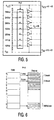
- Fig. 5 shows the generation of partial voltage values for the control of a display in which only 2 rows are controlled at the same time.
- 3 different voltage levels are required, two of which are already given by the two supply voltage levels V LCD and V SS , so that only V 6 has to be generated as a partial voltage value.
- the adaptive selection of the simultaneously controlled rows enables one Reduction of power consumption always the best optical performance for everyone Display size is made possible.
- deswiteren can Driver circuit can be used for many different display sizes, the Requirements for the multiplexibility of the LCD liquid can be reduced.
- the complexity of the driver circuit is not due to changing memory access to complicate at different p values, it requires the memory access sequence to design independently for all values p.
- the sequence of controlling the rows remains the same for all possible numbers p rows to be controlled the same. In particular, the memory access is unchanged.
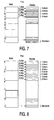
- the sequence the control of the rows is designed for the maximum possible number p and starting the sequences for the lower values p are derived from this value p.
- the first 4 rows of the 8 become maximum simultaneously driven rows and in a second step the others 4 rows driven, whereby memory access is no longer necessary.
- p 2 (Fig. 8) the Control of the 8 rows further divided into 4 by 2 row steps.
- the 8 data bits are read from the memory 9 at one time. This has the advantage that memory access remains unchanged. The addressing of the memory 9 is thus independent from the selection p.
- the sequence of controlling the rows is not always as simple as in the Figures 6 to 8 shown where the first row of the first block also the first line on the Display and this is described from top to bottom. This sequence can do a lot be more complicated.
- the drive deriving mechanism described above lower number p from the maximum allows easy adaptation to the different Functionalities of modern applications such as scrolling, mirroring or compatibility of tape carrier packags TCP versus chip-on-glass applications, this can corresponding logic can be saved and the system is for different display chips easier to adapt.
Landscapes
- Engineering & Computer Science (AREA)
- Theoretical Computer Science (AREA)
- Physics & Mathematics (AREA)
- Crystallography & Structural Chemistry (AREA)
- Computer Hardware Design (AREA)
- General Physics & Mathematics (AREA)
- Chemical & Material Sciences (AREA)
- Control Of Indicators Other Than Cathode Ray Tubes (AREA)
- Liquid Crystal Display Device Control (AREA)
- Liquid Crystal (AREA)
- Circuits Of Receivers In General (AREA)
- Circuit For Audible Band Transducer (AREA)
- Testing, Inspecting, Measuring Of Stereoscopic Televisions And Televisions (AREA)
Abstract
Description
- Fig.1
- eine Prinzipschaltung der erfindungsgemäßen Anzeigevorrichtung.
- Fig.2
- Teilspannungswerte für einen MRA-LCD-Treiber p=8
- Fig.3
- Teilspannungserzeugung für einen LCD-Treiber mit p=8
- Fig.4
- Teilspannungserzeugung für p=4
- Fig.5
- Teilspannungserzeugung für p=2
- Fig. 6
- Auslesesequenz für p=8
- Fig. 7
- Auslesesequenz für p=4
- Fig. 8
- Auslesesequenz für p=2.
| erforderliche VLCD für einen VTH = 1.8 V für Partialanzeigemodus mit adaptiven p Wert | ||||||
| Display Size | N | m | p | F[V] | Gmax[V] | VLCD[V] |
| 16 | 16 | 25 | 2 | 2.55 | 2.55 | 5.1 |
| 24 | 24 | 49 | 2 | 2.55 | 2.55 | 5.1 |
| 32 | 32 | 81 | 2 | 2.55 | 2.55 | 5.1 |
| 40 | 40 | 49 | 4 | 3.29 | 3.29 | 6.58 |
| 48 | 48 | 64 | 4 | 3.33 | 3.33 | 6.66 |
| 56 | 56 | 81 | 4 | 3.38 | 3.38 | 6.76 |
| 64 | 64 | 64 | 8 | 3.85 | 3.85 | 6.70 |
| 80 | 80 | 81 | 8 | 4.02 | 4.02 | 8.04 |
| Teilspannungswerte für unterschiedliche p Werte | ||||
| Bias Level | p=8 | p=4 | p=2 | |
| V1 | VLCD | VLCD | VLCD | Reihen |
| V2 | VLCD | VLCD | VLCD | Spalten |
| V3 | 7/8 VLCD | - | - | Spalten |
| V4 | 3/4 VLCD | 3/4VLCD | - | Spalten |
| V5 | 5/8 VLCD | - | - | Spalten |
| V6 | 1/2 VLCD | 1/2 VLCD | 1/2VLCD | Reihen und Spalten |
| V7 | 3/8 VLCD | - | - | Spalten |
| V8 | 1/4 VLCD | 1/4 VLCD | - | Spalten |
| V9 | 1/8 VLCD | - | - | Spalten |
| V10 | VSS | VSS | VSS | Spalten |
| V11 | VSS | VSS | VSS | Reihen |
Claims (6)
- Anzeigevorrichtungen mit einer Treiberschaltung (1) und einem Display (2) mit mehreren Reihen R und Spalten C, bei dem eine Anzahl p die Zahl der gleichzeitig angesteuerten Reihen angibt und die Reihen R und Spalten C mittels unterschiedlicher Teilspannungswerte der gleichgroßen Spannungen F und GMAX ansteuerbar sind und das Display eine Multiplexibilität von m ≥ R aufweist und die Anzahl p der gleichzeitig angesteuerten Reihen wählbar ist.
- Anzeigevorrichtung nach Anspruch 1, dadurch gekennzeichnet, dass die Treiberschaltung (1) Spannungstreiberstufen (Buffer) enthält, die in Abhängigkeit von der anzusteuernden Displaygröße und der optimalen Anzahl p der gleichzeitig anzusteuernden Reihen abschaltbar sind.
- Anzeigevorrichtung nach Anspruch 1, dadurch gekennzeichnet, dass die optimale Anzahl p aus der Größe des anzusteuerndem Displays oder eines Teilbereichs des Displays ableitbar ist.
- Anzeigevorrichtung nach Anspruch 1, dadurch gekennzeichnet, dass eine Sequenz zur Zuführung der anzuzeigenden Bilddaten aus einem Speicher (9) für alle Werte p gleich ist.
- Anzeigevorrichtung nach Anspruch 1, dadurch gekennzeichnet, dass für einen optimalen Wert p, der kleiner als der maximale Wert pmax ist, die gleichzeitig angesteuerten Reihen p in pmax/p Teilbereiche teilbar sind.
- Treiberschaltung mit mehreren Spannungstreiberstufen zur Erzeugung von mehreren Teilspannungswerten zur Ansteuerung eines Displays mit Reihen R und Spalten C, bei der Spannungstreiberstufen in Abhängigkeit der Displaygpöße und einer davon abhängigen optimalen Anzahl p der gleichzeitig angesteuerten Reihen auswählbar und abschaltbar sind.
Applications Claiming Priority (2)
| Application Number | Priority Date | Filing Date | Title |
|---|---|---|---|
| DE10059768 | 2000-11-30 | ||
| DE10059768A DE10059768A1 (de) | 2000-11-30 | 2000-11-30 | Anzeigevorrichtung mit adaptiver Auswahl der Anzahl der gleichzeitig angezeigten Reihen |
Publications (3)
| Publication Number | Publication Date |
|---|---|
| EP1213700A2 true EP1213700A2 (de) | 2002-06-12 |
| EP1213700A3 EP1213700A3 (de) | 2003-09-10 |
| EP1213700B1 EP1213700B1 (de) | 2006-07-26 |
Family
ID=7665441
Family Applications (1)
| Application Number | Title | Priority Date | Filing Date |
|---|---|---|---|
| EP01000676A Expired - Lifetime EP1213700B1 (de) | 2000-11-30 | 2001-11-29 | Anzeigevorrichtung mit adaptiver Auswahl der Anzahl gleichzeitig angezeigten Reihen |
Country Status (6)
| Country | Link |
|---|---|
| US (1) | US6882332B2 (de) |
| EP (1) | EP1213700B1 (de) |
| JP (1) | JP4230693B2 (de) |
| KR (1) | KR100875826B1 (de) |
| AT (1) | ATE334463T1 (de) |
| DE (2) | DE10059768A1 (de) |
Cited By (1)
| Publication number | Priority date | Publication date | Assignee | Title |
|---|---|---|---|---|
| EP2104094A1 (de) * | 2008-03-17 | 2009-09-23 | The Swatch Group Research and Development Ltd. | Anzeigevorrichtung, die in einem Sondermodus zur Anzeige mit geringem Energieverbrauch betrieben werden kann |
Families Citing this family (8)
| Publication number | Priority date | Publication date | Assignee | Title |
|---|---|---|---|---|
| KR20040071194A (ko) * | 2001-12-14 | 2004-08-11 | 코닌클리즈케 필립스 일렉트로닉스 엔.브이. | 액정 디스플레이 장치 |
| JPWO2004029918A1 (ja) * | 2002-09-25 | 2006-01-26 | シチズン時計株式会社 | 表示装置 |
| US7471272B2 (en) * | 2003-02-19 | 2008-12-30 | Nxp B.V. | Control method and device for a display device |
| US7302797B2 (en) * | 2005-05-31 | 2007-12-04 | Caterpillar Inc. | Hydraulic system having a post-pressure compensator |
| KR20080010789A (ko) * | 2006-07-28 | 2008-01-31 | 삼성전자주식회사 | 표시 장치 및 표시 장치의 구동 방법 |
| DE102007013989B4 (de) | 2007-03-23 | 2009-01-02 | Siemens Ag | Treiberschaltung zur zeilen- und spaltenweisen Ansteuerung einer Passiv-Matrix-Flüssigkristallanzeige |
| CN102789303A (zh) | 2011-05-19 | 2012-11-21 | 国际商业机器公司 | 用于移动终端的节电方法和系统 |
| KR102265988B1 (ko) | 2021-01-29 | 2021-06-16 | (주)피데스 개발 | 주택 상품 개발 시스템 |
Family Cites Families (15)
| Publication number | Priority date | Publication date | Assignee | Title |
|---|---|---|---|---|
| US6057814A (en) * | 1993-05-24 | 2000-05-02 | Display Science, Inc. | Electrostatic video display drive circuitry and displays incorporating same |
| JPH07281632A (ja) * | 1994-04-04 | 1995-10-27 | Casio Comput Co Ltd | 液晶表示装置 |
| JP2690685B2 (ja) * | 1994-04-18 | 1997-12-10 | 静岡日本電気株式会社 | 表示機能付携帯無線機 |
| JPH0876093A (ja) * | 1994-09-08 | 1996-03-22 | Texas Instr Japan Ltd | 液晶パネル駆動装置 |
| JP2642328B2 (ja) | 1995-04-17 | 1997-08-20 | 株式会社トラバース | セメントミルク製造用プラント |
| CN1162736C (zh) * | 1995-12-14 | 2004-08-18 | 精工爱普生株式会社 | 显示装置的驱动方法、显示装置及电子装置 |
| US5859625A (en) * | 1997-01-13 | 1999-01-12 | Motorola, Inc. | Display driver having a low power mode |
| JP3572473B2 (ja) * | 1997-01-30 | 2004-10-06 | 株式会社ルネサステクノロジ | 液晶表示制御装置 |
| JP3411494B2 (ja) * | 1997-02-26 | 2003-06-03 | シャープ株式会社 | マトリクス型表示装置の駆動用電圧生成回路 |
| US6118425A (en) * | 1997-03-19 | 2000-09-12 | Hitachi, Ltd. | Liquid crystal display and driving method therefor |
| WO1999010869A2 (en) * | 1997-08-26 | 1999-03-04 | Koninklijke Philips Electronics N.V. | Display device |
| DE19882734B4 (de) * | 1997-10-09 | 2010-02-11 | Optrex Corp. | Verfahren zum Ansteuern einer einfachen Matrix-Flüssigkristall-Anzeigevorrichtung |
| KR100513910B1 (ko) * | 1998-02-23 | 2005-09-13 | 세이코 엡슨 가부시키가이샤 | 전기 광학 장치의 구동 방법, 전기 광학 장치의 구동 회로, 전기 광학 장치 및 전자 기기 |
| US6323849B1 (en) * | 1999-01-22 | 2001-11-27 | Motorola, Inc. | Display module with reduced power consumption |
| IL135932A0 (en) * | 1999-05-04 | 2001-05-20 | Varintelligent Bvi Ltd | A driving scheme for liquid crystal display |
-
2000
- 2000-11-30 DE DE10059768A patent/DE10059768A1/de not_active Ceased
-
2001
- 2001-11-29 KR KR1020010074822A patent/KR100875826B1/ko not_active Expired - Fee Related
- 2001-11-29 AT AT01000676T patent/ATE334463T1/de not_active IP Right Cessation
- 2001-11-29 US US09/998,055 patent/US6882332B2/en not_active Expired - Lifetime
- 2001-11-29 DE DE50110537T patent/DE50110537D1/de not_active Expired - Fee Related
- 2001-11-29 EP EP01000676A patent/EP1213700B1/de not_active Expired - Lifetime
- 2001-11-30 JP JP2001366462A patent/JP4230693B2/ja not_active Expired - Fee Related
Cited By (3)
| Publication number | Priority date | Publication date | Assignee | Title |
|---|---|---|---|---|
| EP2104094A1 (de) * | 2008-03-17 | 2009-09-23 | The Swatch Group Research and Development Ltd. | Anzeigevorrichtung, die in einem Sondermodus zur Anzeige mit geringem Energieverbrauch betrieben werden kann |
| EP2104092A1 (de) * | 2008-03-17 | 2009-09-23 | The Swatch Group Research and Development Ltd. | Anzeigevorrichtung, die in einem Sondermodus zur Anzeige mit geringem Energieverbrauch betrieben werden kann |
| US8259035B2 (en) | 2008-03-17 | 2012-09-04 | The Swatch Group Research And Development, Ltd. | Display device able to operate in low power partial display mode |
Also Published As
| Publication number | Publication date |
|---|---|
| DE10059768A1 (de) | 2002-06-13 |
| JP2002244628A (ja) | 2002-08-30 |
| EP1213700A3 (de) | 2003-09-10 |
| DE50110537D1 (de) | 2006-09-07 |
| KR20020059225A (ko) | 2002-07-12 |
| ATE334463T1 (de) | 2006-08-15 |
| JP4230693B2 (ja) | 2009-02-25 |
| EP1213700B1 (de) | 2006-07-26 |
| KR100875826B1 (ko) | 2008-12-24 |
| US6882332B2 (en) | 2005-04-19 |
| US20020135551A1 (en) | 2002-09-26 |
Similar Documents
| Publication | Publication Date | Title |
|---|---|---|
| DE60132540T2 (de) | Anzeige, steuerverfahren dafür und tragbares endgerät | |
| DE69416244T2 (de) | Anordnung zur Reduzierung der Leistungsaufnahme in einer Matrixanzeige mit Bildveränderungsdetektion | |
| DE60026649T2 (de) | Anzeigegerät | |
| DE69935285T2 (de) | Elektrooptische vorrichtung und verfahren zu ihrer steuerung, flüssigkristallvorrichtung und verfahren zu ihrer steuerung, treiberschaltung für elektrooptische vorrichtung und elektronisches gerät | |
| DE60131819T2 (de) | Flüssigkristallanzeige mit aktiver Matrix und Steuerverfahren dafür | |
| DE60104927T2 (de) | Flüssigkristallanzeige mit auf digitalen Daten basierten Graustufen, tragbares Telefon und tragbarer persönlicher Hilfsrechner | |
| DE102004040987B4 (de) | Matrix-Display mit adressierbaren Display-Elementen und Verfahren | |
| DE10329088B4 (de) | Flachdisplay zur Anwendung bei einem kleinen Modul | |
| DE69524145T2 (de) | Durch verschiedene stromversorgungen gespeiste integrierte schaltung | |
| DE60121650T2 (de) | Verfahren und Einrichtung zur Graustufensteuerung von Anzeigetafeln | |
| DE102020116090A1 (de) | Elektrolumineszenzanzeigefeld mit einer Pixelansteuerschaltung | |
| DE60004477T2 (de) | Verbesserter spannungspegelumsetzer | |
| DE102011122574A1 (de) | Flüssigkristallanzeigevorrichtung | |
| DE102004057518A1 (de) | Schieberegister und Treiberverfahren für dieses sowie LCD-Treibervorrichtung mit einem solchen | |
| DE102011089176A1 (de) | Treiber, Bildschirmtreiberschaltung und Verfahren zum Betreiben einer Bildschirmtreiberschaltung | |
| DE3526321A1 (de) | Fluessigkristall-anzeigevorrichtung | |
| EP1213700A2 (de) | Anzeigevorrichtung mit adaptiver Auswahl der Anzahl gleichzeitig angezeigten Reihen | |
| DE102006059140A1 (de) | Flüssigkristallanzeigevorrichtung und Verfahren zum Ansteuern derselben | |
| DE112010006031T5 (de) | LCD - Panel und Verfahren zu dessen Herstellung | |
| DE102023132595A1 (de) | Gate-Treiberschaltung und Anzeigepaneel | |
| DE102004050392A1 (de) | Treibersystem für eine Flüssigkristallanzeige | |
| DE60205636T2 (de) | Anzeigevorrichtung mit einer pixel-matrix, die die speicherung von daten erlaubt | |
| DE4428157A1 (de) | Verfahren und Vorrichtung zum Herabsetzen der Speicheranforderungen in einem Anzeigesystem | |
| DE602005002754T2 (de) | Flüssigkristall-matrixanzeige | |
| DE10160098A1 (de) | Anordnung zur Ansteuerung einer Anzeigevorrichtung |
Legal Events
| Date | Code | Title | Description |
|---|---|---|---|
| PUAI | Public reference made under article 153(3) epc to a published international application that has entered the european phase |
Free format text: ORIGINAL CODE: 0009012 |
|
| AK | Designated contracting states |
Kind code of ref document: A2 Designated state(s): AT BE CH CY DE DK ES FI FR GB GR IE IT LI LU MC NL PT SE TR |
|
| AX | Request for extension of the european patent |
Free format text: AL;LT;LV;MK;RO;SI |
|
| RAP1 | Party data changed (applicant data changed or rights of an application transferred) |
Owner name: KONINKLIJKE PHILIPS ELECTRONICS N.V. Owner name: PHILIPS CORPORATE INTELLECTUAL PROPERTY GMBH |
|
| RAP1 | Party data changed (applicant data changed or rights of an application transferred) |
Owner name: PHILIPS INTELLECTUAL PROPERTY & STANDARDS GMBH Owner name: KONINKLIJKE PHILIPS ELECTRONICS N.V. |
|
| PUAL | Search report despatched |
Free format text: ORIGINAL CODE: 0009013 |
|
| AK | Designated contracting states |
Kind code of ref document: A3 Designated state(s): AT BE CH CY DE DK ES FI FR GB GR IE IT LI LU MC NL PT SE TR |
|
| AX | Request for extension of the european patent |
Extension state: AL LT LV MK RO SI |
|
| 17P | Request for examination filed |
Effective date: 20040310 |
|
| AKX | Designation fees paid |
Designated state(s): AT BE CH CY DE DK ES FI FR GB GR IE IT LI LU MC NL PT SE TR |
|
| 17Q | First examination report despatched |
Effective date: 20040512 |
|
| GRAP | Despatch of communication of intention to grant a patent |
Free format text: ORIGINAL CODE: EPIDOSNIGR1 |
|
| GRAS | Grant fee paid |
Free format text: ORIGINAL CODE: EPIDOSNIGR3 |
|
| GRAA | (expected) grant |
Free format text: ORIGINAL CODE: 0009210 |
|
| AK | Designated contracting states |
Kind code of ref document: B1 Designated state(s): AT BE CH CY DE DK ES FI FR GB GR IE IT LI LU MC NL PT SE TR |
|
| PG25 | Lapsed in a contracting state [announced via postgrant information from national office to epo] |
Ref country code: IT Free format text: LAPSE BECAUSE OF FAILURE TO SUBMIT A TRANSLATION OF THE DESCRIPTION OR TO PAY THE FEE WITHIN THE PRESCRIBED TIME-LIMIT;WARNING: LAPSES OF ITALIAN PATENTS WITH EFFECTIVE DATE BEFORE 2007 MAY HAVE OCCURRED AT ANY TIME BEFORE 2007. THE CORRECT EFFECTIVE DATE MAY BE DIFFERENT FROM THE ONE RECORDED. Effective date: 20060726 Ref country code: IE Free format text: LAPSE BECAUSE OF FAILURE TO SUBMIT A TRANSLATION OF THE DESCRIPTION OR TO PAY THE FEE WITHIN THE PRESCRIBED TIME-LIMIT Effective date: 20060726 Ref country code: FI Free format text: LAPSE BECAUSE OF FAILURE TO SUBMIT A TRANSLATION OF THE DESCRIPTION OR TO PAY THE FEE WITHIN THE PRESCRIBED TIME-LIMIT Effective date: 20060726 Ref country code: NL Free format text: LAPSE BECAUSE OF FAILURE TO SUBMIT A TRANSLATION OF THE DESCRIPTION OR TO PAY THE FEE WITHIN THE PRESCRIBED TIME-LIMIT Effective date: 20060726 |
|
| REG | Reference to a national code |
Ref country code: GB Ref legal event code: FG4D Free format text: NOT ENGLISH |
|
| REG | Reference to a national code |
Ref country code: CH Ref legal event code: EP |
|
| REG | Reference to a national code |
Ref country code: IE Ref legal event code: FG4D Free format text: LANGUAGE OF EP DOCUMENT: GERMAN |
|
| REF | Corresponds to: |
Ref document number: 50110537 Country of ref document: DE Date of ref document: 20060907 Kind code of ref document: P |
|
| GBT | Gb: translation of ep patent filed (gb section 77(6)(a)/1977) |
Effective date: 20060913 |
|
| PG25 | Lapsed in a contracting state [announced via postgrant information from national office to epo] |
Ref country code: DK Free format text: LAPSE BECAUSE OF FAILURE TO SUBMIT A TRANSLATION OF THE DESCRIPTION OR TO PAY THE FEE WITHIN THE PRESCRIBED TIME-LIMIT Effective date: 20061026 Ref country code: SE Free format text: LAPSE BECAUSE OF FAILURE TO SUBMIT A TRANSLATION OF THE DESCRIPTION OR TO PAY THE FEE WITHIN THE PRESCRIBED TIME-LIMIT Effective date: 20061026 |
|
| PG25 | Lapsed in a contracting state [announced via postgrant information from national office to epo] |
Ref country code: ES Free format text: LAPSE BECAUSE OF FAILURE TO SUBMIT A TRANSLATION OF THE DESCRIPTION OR TO PAY THE FEE WITHIN THE PRESCRIBED TIME-LIMIT Effective date: 20061106 |
|
| PG25 | Lapsed in a contracting state [announced via postgrant information from national office to epo] |
Ref country code: BE Free format text: LAPSE BECAUSE OF NON-PAYMENT OF DUE FEES Effective date: 20061130 Ref country code: MC Free format text: LAPSE BECAUSE OF NON-PAYMENT OF DUE FEES Effective date: 20061130 Ref country code: LI Free format text: LAPSE BECAUSE OF NON-PAYMENT OF DUE FEES Effective date: 20061130 Ref country code: CH Free format text: LAPSE BECAUSE OF NON-PAYMENT OF DUE FEES Effective date: 20061130 |
|
| PG25 | Lapsed in a contracting state [announced via postgrant information from national office to epo] |
Ref country code: PT Free format text: LAPSE BECAUSE OF FAILURE TO SUBMIT A TRANSLATION OF THE DESCRIPTION OR TO PAY THE FEE WITHIN THE PRESCRIBED TIME-LIMIT Effective date: 20061226 |
|
| NLV1 | Nl: lapsed or annulled due to failure to fulfill the requirements of art. 29p and 29m of the patents act | ||
| REG | Reference to a national code |
Ref country code: GB Ref legal event code: 732E |
|
| REG | Reference to a national code |
Ref country code: IE Ref legal event code: FD4D |
|
| ET | Fr: translation filed | ||
| REG | Reference to a national code |
Ref country code: FR Ref legal event code: TP |
|
| PLBE | No opposition filed within time limit |
Free format text: ORIGINAL CODE: 0009261 |
|
| STAA | Information on the status of an ep patent application or granted ep patent |
Free format text: STATUS: NO OPPOSITION FILED WITHIN TIME LIMIT |
|
| 26N | No opposition filed |
Effective date: 20070427 |
|
| REG | Reference to a national code |
Ref country code: CH Ref legal event code: PL |
|
| BERE | Be: lapsed |
Owner name: PHILIPS INTELLECTUAL PROPERTY & STANDARDS G.M.B.H. Effective date: 20061130 Owner name: KONINKLIJKE PHILIPS ELECTRONICS N.V. Effective date: 20061130 |
|
| PG25 | Lapsed in a contracting state [announced via postgrant information from national office to epo] |
Ref country code: AT Free format text: LAPSE BECAUSE OF NON-PAYMENT OF DUE FEES Effective date: 20061129 |
|
| PG25 | Lapsed in a contracting state [announced via postgrant information from national office to epo] |
Ref country code: GR Free format text: LAPSE BECAUSE OF FAILURE TO SUBMIT A TRANSLATION OF THE DESCRIPTION OR TO PAY THE FEE WITHIN THE PRESCRIBED TIME-LIMIT Effective date: 20061027 |
|
| PG25 | Lapsed in a contracting state [announced via postgrant information from national office to epo] |
Ref country code: LU Free format text: LAPSE BECAUSE OF NON-PAYMENT OF DUE FEES Effective date: 20061129 Ref country code: TR Free format text: LAPSE BECAUSE OF FAILURE TO SUBMIT A TRANSLATION OF THE DESCRIPTION OR TO PAY THE FEE WITHIN THE PRESCRIBED TIME-LIMIT Effective date: 20060726 |
|
| PG25 | Lapsed in a contracting state [announced via postgrant information from national office to epo] |
Ref country code: CY Free format text: LAPSE BECAUSE OF FAILURE TO SUBMIT A TRANSLATION OF THE DESCRIPTION OR TO PAY THE FEE WITHIN THE PRESCRIBED TIME-LIMIT Effective date: 20060726 |
|
| REG | Reference to a national code |
Ref country code: DE Ref legal event code: R084 Ref document number: 50110537 Country of ref document: DE Effective date: 20110426 Ref country code: DE Ref legal event code: R084 Ref document number: 50110537 Country of ref document: DE Effective date: 20111202 |
|
| REG | Reference to a national code |
Ref country code: FR Ref legal event code: TP Owner name: TRIDENT MICROSYSTEMS (FAR EAST) LTD., KY Effective date: 20120418 |
|
| REG | Reference to a national code |
Ref country code: DE Ref legal event code: R119 Ref document number: 50110537 Country of ref document: DE Ref country code: DE Ref legal event code: R409 Ref document number: 50110537 Country of ref document: DE |
|
| REG | Reference to a national code |
Ref country code: DE Ref legal event code: R082 Ref document number: 50110537 Country of ref document: DE Representative=s name: EPPING HERMANN FISCHER, PATENTANWALTSGESELLSCH, DE |
|
| REG | Reference to a national code |
Ref country code: DE Ref legal event code: R082 Ref document number: 50110537 Country of ref document: DE Representative=s name: EPPING HERMANN FISCHER, PATENTANWALTSGESELLSCH, DE Effective date: 20121023 Ref country code: DE Ref legal event code: R081 Ref document number: 50110537 Country of ref document: DE Owner name: ENTROPIC COMMUNICATIONS, INC., US Free format text: FORMER OWNER: TRIDENT MICROSYSTEMS (FAR EAST) LTD., GRAND CAYMAN, KY Effective date: 20121023 Ref country code: DE Ref legal event code: R081 Ref document number: 50110537 Country of ref document: DE Owner name: ENTROPIC COMMUNICATIONS, INC., SAN DIEGO, US Free format text: FORMER OWNER: TRIDENT MICROSYSTEMS (FAR EAST) LTD., GRAND CAYMAN, KY Effective date: 20121023 Ref country code: DE Ref legal event code: R082 Ref document number: 50110537 Country of ref document: DE Representative=s name: EPPING HERMANN FISCHER PATENTANWALTSGESELLSCHA, DE Effective date: 20121023 |
|
| REG | Reference to a national code |
Ref country code: DE Ref legal event code: R119 Ref document number: 50110537 Country of ref document: DE Ref country code: DE Ref legal event code: R409 Ref document number: 50110537 Country of ref document: DE |
|
| REG | Reference to a national code |
Ref country code: DE Ref legal event code: R409 Ref document number: 50110537 Country of ref document: DE |
|
| REG | Reference to a national code |
Ref country code: DE Ref legal event code: R119 Ref document number: 50110537 Country of ref document: DE Effective date: 20120620 Ref country code: DE Ref legal event code: R119 Ref document number: 50110537 Country of ref document: DE Effective date: 20130601 |
|
| PG25 | Lapsed in a contracting state [announced via postgrant information from national office to epo] |
Ref country code: DE Free format text: LAPSE BECAUSE OF NON-PAYMENT OF DUE FEES Effective date: 20130601 |
|
| REG | Reference to a national code |
Ref country code: FR Ref legal event code: TP Owner name: ENTROPIC COMMUNICATIONS, INC., US Effective date: 20131119 |
|
| PGRI | Patent reinstated in contracting state [announced from national office to epo] |
Ref country code: DE Effective date: 20130729 |
|
| PGFP | Annual fee paid to national office [announced via postgrant information from national office to epo] |
Ref country code: GB Payment date: 20141127 Year of fee payment: 14 Ref country code: FR Payment date: 20141118 Year of fee payment: 14 |
|
| GBPC | Gb: european patent ceased through non-payment of renewal fee |
Effective date: 20151129 |
|
| REG | Reference to a national code |
Ref country code: FR Ref legal event code: ST Effective date: 20160729 |
|
| PG25 | Lapsed in a contracting state [announced via postgrant information from national office to epo] |
Ref country code: GB Free format text: LAPSE BECAUSE OF NON-PAYMENT OF DUE FEES Effective date: 20151129 |
|
| PG25 | Lapsed in a contracting state [announced via postgrant information from national office to epo] |
Ref country code: FR Free format text: LAPSE BECAUSE OF NON-PAYMENT OF DUE FEES Effective date: 20151130 |
|
| REG | Reference to a national code |
Ref country code: DE Ref legal event code: R082 Ref document number: 50110537 Country of ref document: DE Representative=s name: PATERIS THEOBALD ELBEL FISCHER, PATENTANWAELTE, DE Ref country code: DE Ref legal event code: R081 Ref document number: 50110537 Country of ref document: DE Owner name: DYNAMIC DATA TECHNOLOGIES, LLC (N.D.GES.D. STA, US Free format text: FORMER OWNER: ENTROPIC COMMUNICATIONS, INC., SAN DIEGO, CALIF., US |
|
| PGFP | Annual fee paid to national office [announced via postgrant information from national office to epo] |
Ref country code: DE Payment date: 20200728 Year of fee payment: 20 |
|
| REG | Reference to a national code |
Ref country code: DE Ref legal event code: R071 Ref document number: 50110537 Country of ref document: DE |