EP1213751A2 - Halbleiterbaugruppe mit einer Verbindungsstruktur - Google Patents
Halbleiterbaugruppe mit einer Verbindungsstruktur Download PDFInfo
- Publication number
- EP1213751A2 EP1213751A2 EP01000680A EP01000680A EP1213751A2 EP 1213751 A2 EP1213751 A2 EP 1213751A2 EP 01000680 A EP01000680 A EP 01000680A EP 01000680 A EP01000680 A EP 01000680A EP 1213751 A2 EP1213751 A2 EP 1213751A2
- Authority
- EP
- European Patent Office
- Prior art keywords
- substrate
- connection structure
- component
- chip
- integrated circuit
- Prior art date
- Legal status (The legal status is an assumption and is not a legal conclusion. Google has not performed a legal analysis and makes no representation as to the accuracy of the status listed.)
- Withdrawn
Links
Images

Classifications
-
- H—ELECTRICITY
- H10—SEMICONDUCTOR DEVICES; ELECTRIC SOLID-STATE DEVICES NOT OTHERWISE PROVIDED FOR
- H10W—GENERIC PACKAGES, INTERCONNECTIONS, CONNECTORS OR OTHER CONSTRUCTIONAL DETAILS OF DEVICES COVERED BY CLASS H10
- H10W72/00—Interconnections or connectors in packages
-
- H—ELECTRICITY
- H10—SEMICONDUCTOR DEVICES; ELECTRIC SOLID-STATE DEVICES NOT OTHERWISE PROVIDED FOR
- H10W—GENERIC PACKAGES, INTERCONNECTIONS, CONNECTORS OR OTHER CONSTRUCTIONAL DETAILS OF DEVICES COVERED BY CLASS H10
- H10W72/00—Interconnections or connectors in packages
- H10W72/20—Bump connectors, e.g. solder bumps or copper pillars; Dummy bumps; Thermal bumps
-
- H—ELECTRICITY
- H10—SEMICONDUCTOR DEVICES; ELECTRIC SOLID-STATE DEVICES NOT OTHERWISE PROVIDED FOR
- H10W—GENERIC PACKAGES, INTERCONNECTIONS, CONNECTORS OR OTHER CONSTRUCTIONAL DETAILS OF DEVICES COVERED BY CLASS H10
- H10W20/00—Interconnections in chips, wafers or substrates
- H10W20/40—Interconnections external to wafers or substrates, e.g. back-end-of-line [BEOL] metallisations or vias connecting to gate electrodes
-
- H—ELECTRICITY
- H10—SEMICONDUCTOR DEVICES; ELECTRIC SOLID-STATE DEVICES NOT OTHERWISE PROVIDED FOR
- H10W—GENERIC PACKAGES, INTERCONNECTIONS, CONNECTORS OR OTHER CONSTRUCTIONAL DETAILS OF DEVICES COVERED BY CLASS H10
- H10W72/00—Interconnections or connectors in packages
- H10W72/071—Connecting or disconnecting
- H10W72/074—Connecting or disconnecting of anisotropic conductive adhesives
-
- H—ELECTRICITY
- H10—SEMICONDUCTOR DEVICES; ELECTRIC SOLID-STATE DEVICES NOT OTHERWISE PROVIDED FOR
- H10W—GENERIC PACKAGES, INTERCONNECTIONS, CONNECTORS OR OTHER CONSTRUCTIONAL DETAILS OF DEVICES COVERED BY CLASS H10
- H10W72/00—Interconnections or connectors in packages
- H10W72/20—Bump connectors, e.g. solder bumps or copper pillars; Dummy bumps; Thermal bumps
- H10W72/231—Shapes
- H10W72/234—Cross-sectional shape, i.e. in side view
-
- H—ELECTRICITY
- H10—SEMICONDUCTOR DEVICES; ELECTRIC SOLID-STATE DEVICES NOT OTHERWISE PROVIDED FOR
- H10W—GENERIC PACKAGES, INTERCONNECTIONS, CONNECTORS OR OTHER CONSTRUCTIONAL DETAILS OF DEVICES COVERED BY CLASS H10
- H10W72/00—Interconnections or connectors in packages
- H10W72/20—Bump connectors, e.g. solder bumps or copper pillars; Dummy bumps; Thermal bumps
- H10W72/251—Materials
-
- H—ELECTRICITY
- H10—SEMICONDUCTOR DEVICES; ELECTRIC SOLID-STATE DEVICES NOT OTHERWISE PROVIDED FOR
- H10W—GENERIC PACKAGES, INTERCONNECTIONS, CONNECTORS OR OTHER CONSTRUCTIONAL DETAILS OF DEVICES COVERED BY CLASS H10
- H10W72/00—Interconnections or connectors in packages
- H10W72/20—Bump connectors, e.g. solder bumps or copper pillars; Dummy bumps; Thermal bumps
- H10W72/261—Functions other than electrical connecting
-
- H—ELECTRICITY
- H10—SEMICONDUCTOR DEVICES; ELECTRIC SOLID-STATE DEVICES NOT OTHERWISE PROVIDED FOR
- H10W—GENERIC PACKAGES, INTERCONNECTIONS, CONNECTORS OR OTHER CONSTRUCTIONAL DETAILS OF DEVICES COVERED BY CLASS H10
- H10W72/00—Interconnections or connectors in packages
- H10W72/30—Die-attach connectors
- H10W72/321—Structures or relative sizes of die-attach connectors
- H10W72/325—Die-attach connectors having a filler embedded in a matrix
-
- H—ELECTRICITY
- H10—SEMICONDUCTOR DEVICES; ELECTRIC SOLID-STATE DEVICES NOT OTHERWISE PROVIDED FOR
- H10W—GENERIC PACKAGES, INTERCONNECTIONS, CONNECTORS OR OTHER CONSTRUCTIONAL DETAILS OF DEVICES COVERED BY CLASS H10
- H10W72/00—Interconnections or connectors in packages
- H10W72/30—Die-attach connectors
- H10W72/351—Materials of die-attach connectors
- H10W72/352—Materials of die-attach connectors comprising metals or metalloids, e.g. solders
-
- H—ELECTRICITY
- H10—SEMICONDUCTOR DEVICES; ELECTRIC SOLID-STATE DEVICES NOT OTHERWISE PROVIDED FOR
- H10W—GENERIC PACKAGES, INTERCONNECTIONS, CONNECTORS OR OTHER CONSTRUCTIONAL DETAILS OF DEVICES COVERED BY CLASS H10
- H10W72/00—Interconnections or connectors in packages
- H10W72/30—Die-attach connectors
- H10W72/351—Materials of die-attach connectors
- H10W72/353—Materials of die-attach connectors not comprising solid metals or solid metalloids, e.g. ceramics
- H10W72/354—Materials of die-attach connectors not comprising solid metals or solid metalloids, e.g. ceramics comprising polymers
Definitions
- the invention relates to an assembly equipped with a component and a substrate, wherein the component has a first connection structure and the substrate has a second connection structure have, as well as with a located between the component and the substrate Interlayer.
- Gold bumps in combination with so-called ACF (anisotropic Conductive Films) material can be used.
- ACF anisotropic Conductive Films
- the reason for this is the incompatibility of the two processes.
- the gold bumps are made by plating the chip surface and then lithographic Structuring created. Gold as a precious metal can easily be part of the used Wafer manufacturing equipment contaminating, which has dramatic ramifications for Yield and performance of the wafer can have.
- US 5,563,449 describes a bump made of Pd, Pt or Ni. Between the bump and two additional layers are applied to the Al pad.
- the first intermediate layer is an adhesive layer made of tungsten or an alloy containing tungsten while the second intermediate layer of tungsten and a metal from the group Pd, Pt and Ni with one Contains concentration gradients.
- the disadvantage is that two additional layers have to be applied in this structure and that the second intermediate layer must have a concentrate gradient, which the Separation considerably complicated and the manufacturing process more expensive.
- An object of the present invention is to overcome the disadvantages of the prior art bypass and provide an assembly with a component and a substrate that is inexpensive to manufacture.
- This task is solved by an assembly equipped with a component and with a substrate, the component a first connection structure and the substrate a have second connection structure, and with one between the component and the Intermediate layer located substrate, wherein the first connection structure of the component Contains aluminum.
- the component is a chip with an integrated circuit, which is a top one Has metal layer is.
- bumps By using aluminum as the material for the first connection structure (so-called bumps) can be made in the same factory as the chip with an integrated one Circuit. This eliminates transport costs and logistics simplified.
- connection structures can be sputtered and known photolithographic processes are produced. These processes are cheaper and far less expensive than the process (electroplating) for producing gold-containing ones Interconnect structures. Furthermore, the distances can be determined using these processes between the connection structures are kept smaller. This is for attachment of increasingly complex integrated circuits is an advantage.
- the tracked aluminum-containing connection structures have a uniform Layer thickness up and deviations in the layer thickness of the first connection structures are only in the nm range.
- the first connection structure of the component be directly connected the top metal layer of the integrated circuit is connected.
- connection structure of the component no layers between the top metal layer of the integrated circuit, the Al pads, and the first connection structure of the component are applied.
- the contact can for example simply via a hole in the protective layer of the chip with an integrated Circuit. The hole is made during the manufacture of the first connection structure filled with aluminum.
- the intermediate layer be an ACF (Anisotropic Conductive Film) material contains.
- ACF material that contains a synthetic resin with conductive particles
- conductive particles of the ACF material have a smaller particle diameter. This can increase the density of conductive particles within the ACF material become. This results in a low contact resistance between the component and the substrate.
- the intermediate layer contains a polymeric material.
- the intermediate layer can also be used to produce a compact, coherent Have structure between component and substrate a polymeric material.
- electrical contact is made between the first connection structure and the second connection structure by means of thermocompression bonding.
- the aluminum-containing first connection structures of the component directly with a second connection structure of the substrate, usually with a copper-containing feed line Gold plating, connected.
- the resulting gaps are in this version filled with the polymeric material.
- the substrate is selected from the group of glass and film.
- the finished chips with aluminum-containing connection structures can be left after the factory is immediately mounted on glass (chip-on-glass, COG) or foil (chip-on-foil, COF) become.
- the component is a chip 1 with an integrated circuit.
- the chip 1 contains a semiconducting substrate 2, which has been provided with active regions by means of various growth, implantation and diffusion processes, an insulation layer 3, a protective layer 4 and a contact 5.
- the insulation layer 3, which contains, for example, SiO 2 is used for electrical Isolation of the chip 1 from the metal layers of the integrated circuit, which are applied to the chip 1
- the chip 1 with integrated circuit has contacts 5, which are made of Al, AlSi or AlCu.
- Protective layer 4 which contains SiO 2 , for example, applied.
- Each chip 1 with an integrated circuit has at least one first connection structure 6, the layer thickness of which is preferably between 2 and 6 ⁇ m.
- the first connection structure 6 contains Al, AlSi or AlCu and is connected directly to the integrated circuit of the chip 1 via a contact 5.
- the protective layer 4 has an opening in the region of a contact 5.
- the chip 1 with integrated circuit is in this embodiment with a film as Substrate 7 connected.
- the film can contain polyimide, for example.
- the substrate 7 has at least one second connection structure 8, which preferably contains Cu.
- the second connection structure 8 has a coating 9 made of, for example, Ni / Au.
- the second connection structure 8 including the coating 9 is preferably a height between 10 and 15 ⁇ m.
- the layer thickness of the coating 9 is preferably between 200 and 500 nm.
- the contact between the first connection structure 6 and the second connection structure 8 of the substrate 7 is made by means of an ACF material, which is an intermediate layer 10 between the chip 1 with integrated circuit and the substrate 7 is made.
- the intermediate layer 10 preferably has a layer thickness between 10 and 25 ⁇ m, preferably between 10 and 20 ⁇ m.
- the ACF material contains a synthetic resin 11 with conductive particles 12.
- the conductive particles 12 are, for example, balls made of synthetic resin, which are coated with Au.
- the diameter the conductive particle 12 is preferably between 3 and 5 ⁇ m.
- the first Connection structure 6 of the chip 1 with integrated circuit and the second connection structure 8 of the substrate 7 are not directly with one another in this embodiment connected, but the connection structures 6, 8 have a distance from one another, which should be at most as large as the particle diameter of the conductive particles 12.
- the electrical contact between the first connection structure 6 of the chip 1 with integrated circuit and the second connection structure 8 of the substrate 7 is about the conductive particles 12 are produced, which are located between the two connection structures 6.8.
- FIG. 2 shows a further possible assembly with a component and a substrate 7 shown.
- a chip 1 with an integrated circuit is opened a film mounted as a substrate 7.
- the first connection structure 6 of the chip 1 with an integrated circuit and the second connection structure 8 of the substrate 7 directly connected to one another via thermocompression bonding.
- the coating 9 made of Ni / Au of the second connection structure 8 forms one Interdiffusion layer with good electrical contact.
- the intermediate layer 10 between the substrate 7 and the chip 1 with circuit is in this embodiment with a polymeric material, such as an epoxy resin.
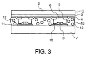
- FIG 3 shows a further assembly according to the invention comprising a component and a substrate 7 shown.
- a chip 1 with an integrated circuit on glass mounted as a substrate 7.
- the second connection structure 8 of the substrate 7 contains therein Embodiment indium-doped tin oxide (ITO).
- ITO Embodiment indium-doped tin oxide
- the electrical contact between the first connection structure 6 and the second connection structure 8 this embodiment via the conductive particles 12 of the ACF material, which is in the intermediate layer 10 between the chip 1 with integrated circuit and the substrate 7 located, manufactured.
- the connection structures 6, 8 in turn assign a distance each other, which corresponds at most to the particle diameter of the conductive particles 12.
- connection structure 6 of the component 1 is arbitrary and can be selected connection technology (thermocompression bonding or use of a ACF materials) can be selected accordingly. So the conductive particles 12 of the ACF material to move away from the area between the connection structures 6,8 migrate. With this connection technology it can be advantageous that the connection structures 6 of component 1 depending on the particle diameter of the conductive particles used Surface depressions from 1 to 4 ⁇ m deep and a diameter between 3 and 10 ⁇ m.
- the connecting structures 6, 8 preferably have a cuboid shape Shape up. The three edge lengths of the cuboid have a size in the ⁇ m range.
Landscapes
- Wire Bonding (AREA)
- Structures For Mounting Electric Components On Printed Circuit Boards (AREA)
Abstract
Description
- Fig. 1
- im Querschnitt einen Chip, der auf Folie montiert ist,
- Fig. 2
- im Querschnitt einen Chip, der mittels Thermokompressions-Bonding auf Folie montiert ist und
- Fig. 3
- Im Querschnitt einen Chip, der auf Glas montiert ist.
Claims (6)
- Baugruppe ausgestattet mit einem Bauteil und einem Substrat (7), wobei das Bauteil eine erste Verbindungsstruktur (6) und das Substrat (7) eine zweite Verbindungsstruktur (8) aufweisen, sowie mit einer zwischen dem Bauteil und dem Substrat befindlichen Zwischenschicht, wobei die erste Verbindungsstruktur (6) des Bauteiles Aluminium enthält.
- Baugruppe nach Anspruch 1,
dadurch gekennzeichnet, dass das Bauteil ein Chip mit integriertem Schaltkreis, welcher eine oberste Metalllage aufweist, ist. - Baugruppe nach Anspruch 2,
dadurch gekennzeichnet, dass die erste Verbindungsstruktur (6) des Bauteiles direkt mit der obersten Metalllage des integrierten Schaltkreises verbunden ist. - Baugruppe nach Anspruch 1,
dadurch gekennzeichnet, dass die Zwischenschicht (10) ein ACF(Anisotropic Conductive Film)-Material enthält. - Baugruppe nach Anspruch 1,
dadurch gekennzeichnet, dass die Zwischenschicht (10) ein polmeres Material enthält. - Baugruppe nach Anspruch 1,
dadurch gekennzeichnet, dass das Substrat (7) ausgewählt ist aus der Gruppe Glas und Folie.
Applications Claiming Priority (2)
| Application Number | Priority Date | Filing Date | Title |
|---|---|---|---|
| DE10059765 | 2000-11-30 | ||
| DE10059765A DE10059765A1 (de) | 2000-11-30 | 2000-11-30 | Baugruppe mit Verbindungsstruktur |
Publications (2)
| Publication Number | Publication Date |
|---|---|
| EP1213751A2 true EP1213751A2 (de) | 2002-06-12 |
| EP1213751A3 EP1213751A3 (de) | 2004-04-21 |
Family
ID=7665439
Family Applications (1)
| Application Number | Title | Priority Date | Filing Date |
|---|---|---|---|
| EP01000680A Withdrawn EP1213751A3 (de) | 2000-11-30 | 2001-11-29 | Halbleiterbaugruppe mit einer Verbindungsstruktur |
Country Status (6)
| Country | Link |
|---|---|
| US (1) | US6617697B2 (de) |
| EP (1) | EP1213751A3 (de) |
| JP (1) | JP2002190496A (de) |
| KR (1) | KR20020042481A (de) |
| DE (1) | DE10059765A1 (de) |
| TW (1) | TW536823B (de) |
Families Citing this family (2)
| Publication number | Priority date | Publication date | Assignee | Title |
|---|---|---|---|---|
| KR20100095268A (ko) * | 2009-02-20 | 2010-08-30 | 삼성전자주식회사 | 반도체 패키지 및 그 제조 방법 |
| TWI671921B (zh) * | 2018-09-14 | 2019-09-11 | 頎邦科技股份有限公司 | 晶片封裝構造及其晶片 |
Family Cites Families (16)
| Publication number | Priority date | Publication date | Assignee | Title |
|---|---|---|---|---|
| JPS59195837A (ja) * | 1983-04-21 | 1984-11-07 | Sharp Corp | Lsiチツプボンデイング方法 |
| US4811081A (en) * | 1987-03-23 | 1989-03-07 | Motorola, Inc. | Semiconductor die bonding with conductive adhesive |
| US5001542A (en) * | 1988-12-05 | 1991-03-19 | Hitachi Chemical Company | Composition for circuit connection, method for connection using the same, and connected structure of semiconductor chips |
| US5323292A (en) * | 1992-10-06 | 1994-06-21 | Hewlett-Packard Company | Integrated multi-chip module having a conformal chip/heat exchanger interface |
| JPH0837190A (ja) * | 1994-07-22 | 1996-02-06 | Nec Corp | 半導体装置 |
| WO1996037913A1 (en) * | 1995-05-22 | 1996-11-28 | Hitachi Chemical Company, Ltd. | Semiconductor device having a semiconductor chip electrically connected to a wiring substrate |
| US5578527A (en) * | 1995-06-23 | 1996-11-26 | Industrial Technology Research Institute | Connection construction and method of manufacturing the same |
| US6328844B1 (en) * | 1996-07-15 | 2001-12-11 | Hitachi Chemical Company, Ltd. | Filmy adhesive for connecting circuits and circuit board |
| US6034331A (en) * | 1996-07-23 | 2000-03-07 | Hitachi Chemical Company, Ltd. | Connection sheet and electrode connection structure for electrically interconnecting electrodes facing each other, and method using the connection sheet |
| US5789278A (en) * | 1996-07-30 | 1998-08-04 | Micron Technology, Inc. | Method for fabricating chip modules |
| JP2825083B2 (ja) * | 1996-08-20 | 1998-11-18 | 日本電気株式会社 | 半導体素子の実装構造 |
| JPH10270624A (ja) * | 1997-03-27 | 1998-10-09 | Toshiba Corp | チップサイズパッケージ及びその製造方法 |
| JP3624729B2 (ja) * | 1998-04-06 | 2005-03-02 | セイコーエプソン株式会社 | Icチップ、ic構造体、液晶装置及び電子機器 |
| JP2000133672A (ja) * | 1998-10-28 | 2000-05-12 | Seiko Epson Corp | 半導体装置及びその製造方法、回路基板並びに電子機器 |
| US6451875B1 (en) * | 1999-10-12 | 2002-09-17 | Sony Chemicals Corporation | Connecting material for anisotropically electroconductive connection |
| US6465879B1 (en) * | 1999-10-19 | 2002-10-15 | Citizen Watch Co., Ltd. | Structure for mounting semiconductor device, method of mounting same, semiconductor device, and method of fabricating same |
-
2000
- 2000-11-30 DE DE10059765A patent/DE10059765A1/de not_active Withdrawn
-
2001
- 2001-11-29 JP JP2001364544A patent/JP2002190496A/ja not_active Withdrawn
- 2001-11-29 EP EP01000680A patent/EP1213751A3/de not_active Withdrawn
- 2001-11-29 KR KR1020010074830A patent/KR20020042481A/ko not_active Withdrawn
- 2001-11-30 US US10/015,720 patent/US6617697B2/en not_active Expired - Lifetime
-
2002
- 2002-01-18 TW TW091100755A patent/TW536823B/zh not_active IP Right Cessation
Also Published As
| Publication number | Publication date |
|---|---|
| EP1213751A3 (de) | 2004-04-21 |
| JP2002190496A (ja) | 2002-07-05 |
| TW536823B (en) | 2003-06-11 |
| KR20020042481A (ko) | 2002-06-05 |
| US20020084517A1 (en) | 2002-07-04 |
| US6617697B2 (en) | 2003-09-09 |
| DE10059765A1 (de) | 2002-06-06 |
Similar Documents
| Publication | Publication Date | Title |
|---|---|---|
| DE10337569B4 (de) | Integrierte Anschlussanordnung und Herstellungsverfahren | |
| DE69523991T2 (de) | Löt-Anschlusskontakt und Verfahren zu seiner Herstellung | |
| DE69526895T2 (de) | Verfahren zur Herstellung einer halbleitenden Anordnung und einer Halbleiterscheibe | |
| DE102008028072B4 (de) | Verfahren zum Herstellen von Halbleitervorrichtungen | |
| DE102013104721B4 (de) | Verfahren für einen verbesserten Anschluss mit geringem Mittenabstand | |
| DE60011702T2 (de) | Verfahren und Struktur zum Verbinden von Schichten in einer Halbleitervorrichtung | |
| DE102018127167B4 (de) | Halbleitervorrichtung mit höckerstruktur und verfahren zum herstellen einer halbleitervorrichtung | |
| DE69500388T2 (de) | Filmschaltungs-Metallsystem zur Verwendung in IC-Bauteilen mit Kontakthöckern | |
| DE102005028951B4 (de) | Anordnung zur elektrischen Verbindung einer Halbleiter-Schaltungsanordnung mit einer äusseren Kontakteinrichtung | |
| DE102008039388A1 (de) | Gestapelte Halbleiterchips | |
| DE112004000360T5 (de) | Zweimetallisches Stud-Bumping für Flipchip-Anwendungen | |
| DE112004001654T5 (de) | Verfahren des Verarbeitens dicker ILD Schichten mit Hilfe von Spritzbeschichten oder Laminieren für einen C4 integrierten Dickmetallprozeßablauf auf Waferebene | |
| DE102016100523B4 (de) | Multi-Stack-Package-on-Package-Strukturen | |
| DE102012213548A1 (de) | Bondpad zum Thermokompressionsbonden, Verfahren zum Herstellen eines Bondpads und Bauelement | |
| WO2009062757A1 (de) | Verfahren zum verbinden zweier fügeflächen | |
| DE10320579A1 (de) | Halbleiterwafer, Nutzen und elektronisches Bauteil mit gestapelten Halbleiterchips, sowie Verfahren zur Herstellung derselben | |
| DE102016118655A1 (de) | Verfahren zur Herstellung von Halbleitervorrichtungen und entsprechende Vorrichtung | |
| DE10227342B4 (de) | Verfahren zur Verbindung einer integrierten Schaltung mit einem Substrat und entsprechende Schaltungsanordnung | |
| DE102006036798B4 (de) | Elektronisches Bauteil und Verfahren zum Herstellen | |
| DE102004047522B3 (de) | Halbleiterchip mit einer Metallbeschichtungsstruktur und Verfahren zur Herstellung desselben | |
| DE102016119676A1 (de) | Verfahren und Halbleiterchipvorrichtung | |
| DE69316159T2 (de) | Verfahren zum Aufbringen von Kontakthöckern auf einer Halbleitervorrichtung sowie zum Verbinden dieser Vorrichtung mit einer Leiterplatte | |
| DE102009001522A1 (de) | Halbleiteranordnung mit Kondensator | |
| DE102014107018A1 (de) | Halbleitervorrichtung mit lötbaren und bondbaren elektrischen Kontaktplättchen | |
| DE102005046737A1 (de) | Bauteil mit Chip-Durchkontakten |
Legal Events
| Date | Code | Title | Description |
|---|---|---|---|
| PUAI | Public reference made under article 153(3) epc to a published international application that has entered the european phase |
Free format text: ORIGINAL CODE: 0009012 |
|
| AK | Designated contracting states |
Kind code of ref document: A2 Designated state(s): AT BE CH CY DE DK ES FI FR GB GR IE IT LI LU MC NL PT SE TR |
|
| AX | Request for extension of the european patent |
Free format text: AL;LT;LV;MK;RO;SI |
|
| RAP1 | Party data changed (applicant data changed or rights of an application transferred) |
Owner name: KONINKLIJKE PHILIPS ELECTRONICS N.V. Owner name: PHILIPS CORPORATE INTELLECTUAL PROPERTY GMBH |
|
| RAP1 | Party data changed (applicant data changed or rights of an application transferred) |
Owner name: KONINKLIJKE PHILIPS ELECTRONICS N.V. Owner name: PHILIPS INTELLECTUAL PROPERTY & STANDARDS GMBH |
|
| PUAL | Search report despatched |
Free format text: ORIGINAL CODE: 0009013 |
|
| AK | Designated contracting states |
Kind code of ref document: A3 Designated state(s): AT BE CH CY DE DK ES FI FR GB GR IE IT LI LU MC NL PT SE TR |
|
| AX | Request for extension of the european patent |
Extension state: AL LT LV MK RO SI |
|
| RIC1 | Information provided on ipc code assigned before grant |
Ipc: 7H 01L 21/60 A |
|
| 17P | Request for examination filed |
Effective date: 20041021 |
|
| 17Q | First examination report despatched |
Effective date: 20041124 |
|
| AKX | Designation fees paid |
Designated state(s): CH DE FR GB LI |
|
| STAA | Information on the status of an ep patent application or granted ep patent |
Free format text: STATUS: THE APPLICATION IS DEEMED TO BE WITHDRAWN |
|
| 18D | Application deemed to be withdrawn |
Effective date: 20051102 |