EP1213795B1 - Elektrischer Verbindersockel mit Auswurfvorrichtung für eine Einsteckkarte - Google Patents
Elektrischer Verbindersockel mit Auswurfvorrichtung für eine Einsteckkarte Download PDFInfo
- Publication number
- EP1213795B1 EP1213795B1 EP02075269A EP02075269A EP1213795B1 EP 1213795 B1 EP1213795 B1 EP 1213795B1 EP 02075269 A EP02075269 A EP 02075269A EP 02075269 A EP02075269 A EP 02075269A EP 1213795 B1 EP1213795 B1 EP 1213795B1
- Authority
- EP
- European Patent Office
- Prior art keywords
- ejector
- daughtercard
- socket
- connector
- engage
- Prior art date
- Legal status (The legal status is an assumption and is not a legal conclusion. Google has not performed a legal analysis and makes no representation as to the accuracy of the status listed.)
- Expired - Lifetime
Links
- 230000014759 maintenance of location Effects 0.000 claims description 29
- 238000003780 insertion Methods 0.000 claims description 23
- 230000037431 insertion Effects 0.000 claims description 23
- 230000008878 coupling Effects 0.000 claims description 5
- 238000010168 coupling process Methods 0.000 claims description 5
- 238000005859 coupling reaction Methods 0.000 claims description 5
- 230000000087 stabilizing effect Effects 0.000 claims description 5
- 238000000605 extraction Methods 0.000 description 7
- 230000010287 polarization Effects 0.000 description 7
- 230000008901 benefit Effects 0.000 description 4
- 230000035939 shock Effects 0.000 description 3
- 230000007246 mechanism Effects 0.000 description 2
- 230000007423 decrease Effects 0.000 description 1
- 238000006073 displacement reaction Methods 0.000 description 1
- 230000006870 function Effects 0.000 description 1
- 238000012986 modification Methods 0.000 description 1
- 230000004048 modification Effects 0.000 description 1
- 229910000679 solder Inorganic materials 0.000 description 1
Images


Classifications
-
- H—ELECTRICITY
- H01—ELECTRIC ELEMENTS
- H01R—ELECTRICALLY-CONDUCTIVE CONNECTIONS; STRUCTURAL ASSOCIATIONS OF A PLURALITY OF MUTUALLY-INSULATED ELECTRICAL CONNECTING ELEMENTS; COUPLING DEVICES; CURRENT COLLECTORS
- H01R12/00—Structural associations of a plurality of mutually-insulated electrical connecting elements, specially adapted for printed circuits, e.g. printed circuit boards [PCB], flat or ribbon cables, or like generally planar structures, e.g. terminal strips, terminal blocks; Coupling devices specially adapted for printed circuits, flat or ribbon cables, or like generally planar structures; Terminals specially adapted for contact with, or insertion into, printed circuits, flat or ribbon cables, or like generally planar structures
- H01R12/70—Coupling devices
- H01R12/7005—Guiding, mounting, polarizing or locking means; Extractors
-
- H—ELECTRICITY
- H01—ELECTRIC ELEMENTS
- H01R—ELECTRICALLY-CONDUCTIVE CONNECTIONS; STRUCTURAL ASSOCIATIONS OF A PLURALITY OF MUTUALLY-INSULATED ELECTRICAL CONNECTING ELEMENTS; COUPLING DEVICES; CURRENT COLLECTORS
- H01R13/00—Details of coupling devices of the kinds covered by groups H01R12/70 or H01R24/00 - H01R33/00
- H01R13/62—Means for facilitating engagement or disengagement of coupling parts or for holding them in engagement
- H01R13/629—Additional means for facilitating engagement or disengagement of coupling parts, e.g. aligning or guiding means, levers, gas pressure electrical locking indicators, manufacturing tolerances
- H01R13/633—Additional means for facilitating engagement or disengagement of coupling parts, e.g. aligning or guiding means, levers, gas pressure electrical locking indicators, manufacturing tolerances for disengagement only
-
- H—ELECTRICITY
- H05—ELECTRIC TECHNIQUES NOT OTHERWISE PROVIDED FOR
- H05K—PRINTED CIRCUITS; CASINGS OR CONSTRUCTIONAL DETAILS OF ELECTRIC APPARATUS; MANUFACTURE OF ASSEMBLAGES OF ELECTRICAL COMPONENTS
- H05K7/00—Constructional details common to different types of electric apparatus
- H05K7/14—Mounting supporting structure in casing or on frame or rack
- H05K7/1401—Mounting supporting structure in casing or on frame or rack comprising clamping or extracting means
- H05K7/1402—Mounting supporting structure in casing or on frame or rack comprising clamping or extracting means for securing or extracting printed circuit boards
- H05K7/1409—Mounting supporting structure in casing or on frame or rack comprising clamping or extracting means for securing or extracting printed circuit boards by lever-type mechanisms
Definitions
- the present invention relates to an electrical connector socket having an ejector mechanism for removing fashionhtercard or module from the socket. More particularly, the present invention relates to an improved electrical connector which provides a retention force when the daughtercard is inserted into the socket and also permits the daughtercard to be easily ejected from the socket when desired.
- SIMM sockets such as Single In-line Memory Module (SIMM) sockets
- the sockets are formed to include an elongated slot and a plurality of electrical terminals coupled to the housing adjacent to the slot.
- conductive surfaces on the daughtercard engage the terminals to couple the daughtercard to the socket electrically.
- the terminals are also coupled to conductive traces on the mother board so that when the daughtercard is inserted into the socket, the daughtercard is electrically coupled to the mother board.
- SIMM socket configurations see, for example, U.S. Patent No. 5,013,264 to Tondreault and U.S. Patent Application Serial No.07/759,409, owned by the assignee of the present invention, and incorporated herein by reference.
- One problem associated with conventional electrical connectors is that it is often difficult to extract a daughtercard that is held in a socket formed in an electrical connector. It is understood that a plurality of sockets may be located adjacent each other with daughtercards in each of the sockets. In such tight quarters it is often difficult for a technician to remove a selected daughtercard from the connector socket manually by hand or using a tool. Unless precautions are taken, the daughtercard can be damaged during extraction of the daughtercard from the socket. Therefore, it is desirable to provide an ejector mechanism coupled to the socket to facilitate ejection of the daughter card from the socket.
- the present invention provides an improved design for an ejector for a single row socket. It is known to provide ejectors for such single row sockets. See, for example, U.S. Patent No. 4,990,097 to Billman, et al.
- the '097 patent discloses a connector having extraction members which can be lifted upwardly relative to the socket to permit a circuit board to be withdrawn from the socket.
- it is often difficult to access the extraction members A great deal of room is required beyond the edge of the extraction members to permit a technician to grip under a ledge of the extraction members and lift.
- a relatively large amount of force must be applied to the extraction members to remove the circuit board from the socket.
- a problem associated with conventional sockets is that the daughtercard tends to dislodge from the socket during handling or during motor or fan vibration. Such dislodging can cause intermittent or failed signal paths between the daughtercard and the mother board.
- An object of the present invention is to facilitate ejection of a daughtercard from a socket, while improving the retention force on the daughtercard to retain the daughtercard in the socket and while facilitating alignment of the daughtercard with the socket during insertion of the daughtercard into the socket.
- an ejector for ejecting a daughtercard from an elongated slot formed in an electrical connector socket housing.
- the ejector includes a body having means for ejecting an end of the daughtercard adjacent the ejector out of the elongated slot upon movement of the ejector relative to the socket housing.
- the body is also formed to include first and second-crimp surfaces for engaging a side edge of the daughtercard to stabilize the daughtercard in the socket.
- means is also provided for biasing the ejector body in a direction toward the daughtercard to hold the first and second crimp surfaces against the daughtercard.
- the biasing means includes first and second wedges formed on opposite side surfaces of the ejector body, and first and second locking tabs formed on the socket housing for engaging the first and second wedges, respectively, to apply a biasing force to the,ejector body in a direction toward the daughtercard.
- the first and second crimp surfaces are illustratively convergent to accommodate daughtercards having various lengths and thicknesses.
- the first and second locking tabs also engage the opposite side surfaces of the ejector body to apply opposing, inwardly directed forces to the ejector body, thereby centralizing and stabilizing the ejector body within the socket housing.
- the ejector further includes first and second raised surfaces formed on the opposite side surfaces of the body of the ejector and configured so that the first and second locking tabs engage the first and second raised surfaces respectively.
- the ejector also includes first and second lead in ramp surfaces formed on the ejector body above the first and second crimp surfaces, respectively. These first and second lead in ramp surfaces reduce the likelihood of stubbing a bottom surface of the daughtercard against the ejector body during insertion of the daughtercard into the socket housing.
- Fig. 1 illustrates a socket 10 which falls outside the scope of the present invention but which is included for illustrative purposes.
- Socket 10 includes a housing 12 formed to include an elongated slot 14 therein for receiving a daughtercard 16.
- Socket 10 includes a plurality of contacts 18 for engaging conductive surfaces on daughtercard 16 when daughtercard 16 is inserted into socket 10.
- Socket 10 includes a first end 20 and an opposite second end 22 spaced apart from first end 20.
- First and second ends 20 and 22 have an identical configuration including a first opening 24 and a second opening 26.
- An ejector 28 is pivotably coupled to first end 20 of socket 10.
- a fixed retention post 30 is coupled to second end 22 of socket 10.
- Fig. 2 illustrates ejector 28 which is configured to retain and to eject daughtercard 16 from socket 10.
- Ejector 28 includes a body portion 32 and a head 34 formed integrally with body portion 32 to facilitate pivotal movement of ejector 28.
- Head 34 provides a "finger shelf” on which to push when actuating ejector 28.
- a pair of axles 35 are formed on opposite sides on body portion 32.
- Axles 35 define a pivot axis 36 which is perpendicular to elongated slot 14 formed along a longitudinal axis of socket 10.
- Body 32 is formed to include a slot 42 therein for receiving an end edge portion of daughtercard 16 as daughtercard 16 is inserted into socket 10.
- a bottom surface 44 of ejector 28 is configured to engage a bottom surface 92 of daughtercard 16 as daughtercard 16 is inserted into socket 10.
- a cross member 45 is formed across slot 42 to provide a polarization member as discussed below.
- Body portion 32 of ejector 28 also includes a pair of flexible spring arms 48 and 50 that project away from body portion 32.
- Arms 48 and 50 are each formed to include tapered heads 52 and 54, respectively, which engage opposite sides of daughtercard 16 to retain daughtercard 16 in socket 10. Side portions of ramp-shaped edge surfaces 56 and 58 of heads 52 and 54 force arms 48 and 50 apart or open during insertion of daughtercard 16 into socket 10.
- the tapered or ramped surfaces 56, 58, 80, and 82 of heads 52, 54, 76, and 78, respectively, provide a "lead in” geometry and stress distribution during displacement.
- the three tapered sides (top and two opposite sides) of ramp surfaces 56, 58, 80, and 82 are provided to retain daughtercard 16 in socket 10 without increasing the insertion force of daughtercard. 16.
- a triangular-shaped wedge 60 is formed on each side of body 32 to help secure ejector within socket 10. As illustrated in Fig. 1, wedges 60 on opposite sides of body portion 32 engage sidewalls 26 of housing 12. Ejector 10 is inserted from the top of socket 10 into openings 24 and 26 until axles 35 snap into the preformed openings 24 and 26 of housing 12.
- Fig. 3 illustrates insert post 30 for forming the rigid, fixed post 30 at second end 22 of socket 10.
- Post 30 includes a body portion 62 and a pair of axles 64 formed on opposite sides of body portion 62.
- the configuration of body portion 62 and axles 64 are similar to the configuration of body portion 32 and axles 35 of ejector 28. Therefore, post 30 can be inserted into either the first or second ends 20 or 22 of socket 10.
- Post 30 does not include a head portion such as head 34 of ejector 28.
- Post 30 does not move relative to socket 10. In other words, post 30 is in a fixed position relative to housing 12.
- Post 30 provides retention means at the opposite end of housing 12 from ejector 28. Post 30 also provides a guide for insertion of daughtercard 16 into socket 10. Post 30 is formed to include a slot 66 for receiving an end edge portion of daughtercard 16 therein as daughtercard 16 is inserted into socket 10. An end edge 93 of daughtercard 16 is aligned with wall 67 of post 30 during insertion of daughtercard 16 into socket 10 to align the plurality of contact surfaces of daughtercard 16 with the plurality of terminals 18 of socket 10.
- Retention post 30 is shown without a polarization cross member 45. It is understood that insert 30 may be formed to include a polarization crass member such as cross member 45 illustrated in Fig. 2. In that instance, ejector 28 at the opposite end of socket-. 10 would not include a cross member 45. Only one polarization cross member 45 is provided. A bottom surface 68 of post 30 engages a bottom surface of daughtercard 16 when daughtercard 16 is fully inserted into socket 10.
- Body portion 62 of post 30 is formed to include a pair of flexible arms 72 and 74 that project away from body portion 62.
- Arms 72 and 74 are each formed to include tapered heads 76 and 78, respectively, which engage opposite sides of daughtercard 16 to retain daughtercard 16 in socket 10.
- a triangular-shaped wedge 84 is formed on each side of body 62 to help secure retention post 30 within socket 10.
- the present invention provides flexibility for inserting ejector 28 and retention post 30 into socket 10. Since socket 10 is symmetrical, ejector 28 and retention post 30 can be selectively inserted into either first end 20 or second end 22 of socket 10. Therefore, although Fig. 1 illustrates the invention with ejector 28 coupled to first end 20 of socket 10 and retention post 30 coupled to second end 22 of socket 10, it is understood that the locations of ejector 28 and retention post 30 could be reversed.
- the provision of fixed retention post 30 opposite from ejector 28 provides numerous advantages during insertion of daughtercard 16 into socket 10 or during removal of daughtercard 16 from socket 10 as discussed below.
- One advantageous feature of socket 10 which includes post 30 and ejector 28 is that socket 10 requires less board space on the mother board.
- Fig. 4 illustrates the configuration of terminals 18 within socket 10 and further illustrates the configuration of ejector 28.
- Terminals 18 include contact surfaces 86 which extend into slot 14 to engage conductive surfaces on opposite sides of daughtercard 16 when daughtercard 16 is inserted into slot 14.
- Terminals 18 also include contact tails 87 for electrically coupling terminals 18 to the mother board (not shown).
- the configuration of terminals 18 is discussed in detail in copending U.S. Patent Application Serial No. 07/759,409, owned by the assignee of the present invention and incorporated herein by reference. It is understood, however, that various other terminal configurations may be used in accordance with the present invention. In other words, the present invention is not limited by the specific configuration of terminals 18.
- Daughtercard 16 is formed to include apertures 88 therein.
- An end edge 93 of daughtercard 16 is first aligned with socket 10 using the fixed retention post 30 as a guide.
- post 30 as an alignment guide for inserting daughtercard 16 advantageously aligns conductive surfaces -on daughtercard 16 with terminals 18 of socket 10. This is an advantage over the device disclosed in U.S. Patent No. 5,074,800 are discussed above.
- the circuit board may become misaligned with the socket due to the end play caused by having ejection levers with the socket at both ends of the socket.
- the present invention advantageously reduces the likelihood of misalignment between daughtercard 16 and socket 10 by providing fixed retention post insert 30 which is used as an insertion alignment guide.
- bottom surface 92 of daughtercard 16 engages bottom surface 44 of ejector 28 and causes rotation of ejector 28 about pivot axis 36 in the direction of arrow 94.
- the ramped surfaces 56 and 58 on heads 52 and 54, respectively, cause arms 48 and 50 to move apart automatically as they contact a side edge 96 of daughtercard 16.
- Ramped heads 56 and 58 enter aperture 88 from opposite sides of daughtercard 16 to stabilize and retain daughtercard 16 within socket 10.
- Heads 76 and 78 of arms 72 and 74, respectively, formed integrally with fixed retention post 30 also enter an aperture 88 of daughtercard 16.
- Daughtercard 16 is illustrated in the fully inserted position in Fig. 6.
- Heads 52 and 54 of ejector 28 and heads 76 and 78 of post 30 are designed to increase retention of daughtercard 16 within socket 10 during movement, vibration or shock of socket 10 which can occur under rigid mechanical conditions, during movement, or during operation of a motor or fan adjacent socket 10.
- Heads 52, 54, 76 and 78 apply both a horizontal retention force and a vertical retention force against daughtercard 16.
- Fig. 7 illustrates engagement of heads 52 and 54 of ejector 28 with daughtercard 16. It is understood that the engagement of heads 76 and 78 of post 30 is identical to the description of heads 52 and 54. Therefore, only a description of heads 52 and 54 will be provided.
- ramped surface 56 of head 52 engages a sidewall defining aperture 88 in daughtercard 16 and spring arm 48 applies a force normal to daughtercard 16 in the direction of arrow 95.
- bottom surface 98 of head 52 provides a downwardly-directed vertical retention force to daughtercard 16 as illustrated by arrow 97 to hold daughtercard 16 in socket 10.
- Ramped surface 58 of head 54 engages an opposite side of daughtercard 16 so that spring arm 50 applies a normal force against daughtercard 16 in the direction of arrow 99. 5
- bottom surface 98 of head 54 enters aperture 88 to provide a downwardly-directed vertical retention force to daughtercard 16 in the-direction of arrow 97.
- Heads 52 and 54 of ejector 28 and heads 76 and 78 of post 30 provide a retention force on daughtercard 16 without the use of a latch which the user must manually displace in order to remove daughtercard 16 from socket 10.
- a computer in which socket 10 is installed can be subjected to an increased amount of shock and vibration due to movement of the computer or due to motor or fan vibration without dislocating daughtercard 16 from socket 10. Therefore, the configuration of socket 10 reduces the likelihood of intermittent or failed signal paths from daughtercard 16 to the mother board while facilitating removal of daughtercard 16 from socket 10.
- Ramped surfaces 56 and 58 of heads 52 and 54 are configured to allow for locational and size tolerances of aperture 88 formed in daughtercard 16.
- ejector 28 When it is desired to remove daughtercard 16 from socket 10, ejector 28 is rotated about pivot axis 36 in the direction of arrow 102 of Fig. 8. This movement of ejector 28 forces the end of daughtercard 16 adjacent ejector 28 to move in the direction of arrow 104 out of socket 10. As illustrated in Fig. 8, an opposite end of daughtercard 16 adjacent post 30 remains in elongated slot 14 of socket 10 during movement of ejector 10 in the direction of arrow 102. Therefore, daughtercard pivots about bottom surface 92 of end edge 93 adjacent post 30 during ejection.
- Figs. 5, 6, and 8 illustrate a polarization notch 106 formed in daughtercard 16 for use with polarization cross member 45 of ejector 28 to polarize daughtercard 16 in socket 10. It is understood that if a cross member is used on post 30 instead of ejector 28 that the polarization of daughtercard 16 would be reversed.
- ejector 134 is formed to include angled crimp surfaces 136 and 138 on spring arms 48 and 50, respectively, in front of daughtercard receiving notch 137.
- Crimp surfaces 136 and 138 are spaced apart further at a first end near heads 52 and 54 than at a second end near head 34 to provide convergent or tapered lead-in surfaces.
- Crimp surfaces 136 and 138 are configured to engage opposite corners of end edge 96 of daughtercard 16 as best illustrated in Fig. 10.
- crimp surfaces 136 and 138 crimp, pinch against, or engage end edge 96 of daughtercard 16 to help stabilize daughtercard 16 within socket 10.
- Ejector 134 is also formed to include a raised surface 140 extending toward head 34 from a locking wedge 142 on each side of body 32.
- socket 10 is formed to include locking tabs 144 and 145 which are configured to engage raised surfaces 140 of ejector 134 so that each tab 144 and 145 applies an inwardly directed force in the direction of arrows 146 and 147, respectively, to stabilize ejector 134 within housing 12. Therefore, the opposing, inwardly directed forces applied to raised surfaces 140 on opposite sides of body 32 of ejector 134 in the directions of arrows 146 and 147 by locking tabs 144 and 145, respectively, centralize and stabilize ejector 134 inside housing 12. This reduces or prohibits side-to-side motion of ejector 134 during shock or vibration of housing 12.
- Locking tabs 144 and 145 move outwardly in the directions of 148 and 149, respectively, as ejector 134 is pivoted within housing 12 in the direction of arrow 94 of Fig. 5 from the outwardly pivoted ejection position Fig. 5 to the upright retention position of Fig. 6. Locking tabs 144 and 145 also move outwardly upon engagement of wedges 142 as ejector moves in the direction of arrow 102 in Fig.8 from the upright retention position to the outwardly pivoted ejection position.
- Wedges 142 have a triangular shape to provide ramps for moving the tabs 144 and 145 outwardly during movement of ejector in either direction.
- Locking tabs 144 and 145 also apply a force to side edges 150 of wedges 142. Therefore, locking tabs 144 and 145 apply force in the direction of arrow 152 to ejector 134 when ejector 134 is in the upright retention position illustrated in Fig. 10 to hold crimp surfaces 136 and 138 against end edge 96 of daughtercard 16, thereby stabilizing daughtercard 16 within socket 10.
- Lead-in ramp surfaces 154 and 156 formed on ejector 134.
- Lead-in ramp surfaces 154 and 156 are located above crimp surfaces 136 and 138, respectively, reduce the likelihood of stubbing a bottom surface 92 of daughtercard 16 against a top edge 158 of ejector 134 during insertion of daughtercard 16 into socket 10.
- Still another feature of the ejector illustrated in Fig. 9 is the provision of lead-in surfaces 160 and 162 formed on heads 52 and 54, respectively.
- Lead-in surfaces 160 and 162 are cut in heads 52 and 54 to facilitate movement of spring arms 48 and 50 away from each other as ejector 134 rotates in the direction of arrow 94 of Fig. 5 during insertion of daughtercard 16.
- lead in ramp surfaces 160 and 162 initially engage side edge 96 of daughtercard 16 and cause spring arrows 48 and 50 to move away from each other and move over daughtercard 16.
- Ramp surfaces 160 and 162 therefore facilitate movement of spring arms 48 and 50 away from each other as ejector 134 rotates to the upright retention position illustrated in Fig. 6.
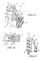
- Figs. 11-13 illustrate another embodiment of a fixed post 170 located at an opposite end of socket 10 or 110 from ejector 28 or 134.
- fixed post 170 is formed integrally with housing 112 of socket 110.
- Fixed post 170 includes an end tower 172 formed to include an elongated slot 174 therein for receiving end edge 93 of daughtercard 16. Therefore, slot 174 provides means for aligning daughtercard 16 relative to socket 110.
- Fixed post 170 is also formed to include a pair of resilient beams 176 and 178 located on opposite sides of the elongated slot 114 of housing 112.
- Resilient stabilizing beams 176 and 178 are formed to include head portions 180 and 182, respectively, for engaging opposite sides of daughtercard 16 upon insertion of daughtercard 16 into socket 110 to stabilize an end of daughtercard adjacent fixed post 170 within socket 110.
- Figs. 12 and 13 5 further illustrate the details of fixed post 170.
Landscapes
- Engineering & Computer Science (AREA)
- Microelectronics & Electronic Packaging (AREA)
- Details Of Connecting Devices For Male And Female Coupling (AREA)
- Coupling Device And Connection With Printed Circuit (AREA)
Claims (31)
- Auswerfer (134) zum Auswerfen einer Tochterkarte (16) aus einem langgestreckten Schlitz (14), der im Buchsengehäuse eines elektrischen Steckers gebildet ist, wobei der Auswerfer einen Körper mit Einrichtungen umfasst, um ein Ende der Tochterkarte neben dem Auswerfer aus dem langgestreckten Schlitz zu werfen, wenn der Auswerfer relativ zum Buchsengehäuse bewegt wird, dadurch gekennzeichnet, dass der Körper außerdem so ausgebildet ist, dass er eine erste und eine zweite Klemmfläche (136, 138) zum Erfassen eines Seitenrandes (96) der Tochterkarte aufweist, um die Tochterkarte in der Buchse zu stabilisieren.
- Auswerfer gemäß Anspruch 1, der weiterhin Einrichtungen (142, 144, 145) zum Vorspannen des Auswerferkörpers in eine Richtung auf die Tochterkarte (16) zu umfasst, um die erste und die zweite Klemmfläche (136, 138) an der Tochterkarte zu halten.
- Auswerfer gemäß Anspruch 2, bei dem die Vorspanneinrichtungen einen ersten und einen zweiten Keil (142), die an den gegenüberliegenden Seitenflächen des Auswerferkörpers (134) ausgebildet sind, und erste und zweite Sperrzungen (144, 145) aufweisen, die am Buchsengehäuse ausgebildet sind, um den ersten bzw. den zweiten Keil in Eingriff zu nehmen und dadurch eine Vorspannkraft an den Auswerferkörper in eine Richtung auf die Tochterkarte (16) zu zu legen.
- Auswerfer gemäß Anspruch 3, bei dem die erste und die zweite Sperrzunge (144, 145) auch die gegenüberliegenden Seitenflächen des Auswerferkörpers (134) in Eingriff nehmen, um einander entgegengesetzte und nach innen gerichtete Kräfte an den Auswerferkörper zu legen und dadurch den Auswerferkörper in dem Buchsengehäuse zu zentralisieren und zu stabilisieren.
- Auswerfer gemäß Anspruch 1, bei dem der Auswerferkörper (134) eine erste und eine zweite gegenüberliegende Seitenfläche (140) aufweist und weiterhin Einrichtungen (144, 145) umfasst, die nach innen gerichtete Kräfte an die erste und die zweite gegenüberliegende Seitenfläche legen, um den Auswerferkörper im Buchsengehäuse zu zentralisieren und zu stabilisieren.
- Auswerfer gemäß Anspruch 5, bei dem die Einrichtungen zum Anlegen von nach innen gerichteten Kräften eine erste und eine zweite Sperrzunge (144, 145) umfassen, die am Buchsengehäuse ausgebildet sind, wobei die erste und die zweite Sperrzunge so ausgebildet sind, dass sie die erste und die zweite gegenüberliegende Seitenfläche (140) des Auswerferkörpers (134) jeweils in Eingriff nehmen.
- Auswerfer gemäß Anspruch 6, welcher weiterhin eine erste und eine zweite hochstehende Fläche (140) umfasst, die an den gegenüberliegenden Seitenflächen des Auswerferkörpers und derart ausgebildet sind, dass die erste und die zweite Sperrzunge (144, 145) die erste und die zweite hochstehende Fläche jeweils in Eingriff nehmen.
- Auswerfer gemäß Anspruch 1, der weiterhin einen ersten und einen zweiten Federarm (48, 50) aufweist, um die gegenüberliegenden Seiten der Tochterkarte (16) zu erfassen und dadurch die Tochterkarte beim Einstecken der Tochterkarte in die Buchse (10) in der Buchse festzuhalten.
- Auswerfer gemäß Anspruch 8, bei dem der erste und der zweite Federarm (48, 50) des Auswerfers (134) jeweils einen Kopfteil (52, 54) aufweisen, der so ausgebildet ist, dass gegenüberliegende Seiten der Tochterkarte (16) erfasst werden und dadurch die Tochterkarte in der Buchse festgehalten wird, wobei die Kopfteile jeweils eine schräg geformte Fläche (160, 162) aufweisen, um den ersten und den zweiten Federarm des Auswerfers beim Einstecken der Tochterkarte in die Buchse (10) automatisch auseinanderzudrücken.
- Auswerfer gemäß Anspruch 8, bei dem die Kopfteile (52, 54) so ausgebildet sind, dass sie in eine Öffnung (88) eintreten, die in der Tochterkarte (16) neben dem Auswerfer (134) von den gegenüberliegenden Seiten der Tochterkarte ausgehend ausgebildet ist, wobei die Kopfteile eine Randfläche, die so ausgebildet ist, dass sie die Tochterkarte erfasst und eine Kraft normal zur Tochterkarte anlegt, und eine Unterfläche aufweist, um eine Kraft gegen die Tochterkarte in Richtung nach unten in den langgestreckten Schlitz (14) des Buchsengehäuses zu legen.
- Auswerfer gemäß Anspruch 1, der weiterhin Einrichtungen (45) zum Polen der Tochterkarte in der Buchse aufweist.
- Auswerfer gemäß Anspruch 1, der weiterhin ein erstes und ein zweites Anschlussbein in den schräg geformten Flächen (154, 156) umfasst, die auf dem Auswerferkörper (134) oberhalb der ersten bzw. der zweiten Klemmfläche (136, 138) ausgebildet sind, um die Gefahr des Anstoßens einer Bodenfläche der Tochterkarte gegen den Auswerferkörper beim Einstecken der Tochterkarte (16) in das Buchsengehäuse zu reduzieren.
- Auswerfer gemäß Anspruch 1, bei dem die erste und die zweite Klemmfläche (136, 138) zusammenlaufen, um Tochterkarten (16) mit verschiedenen Längen und Dicken unterzubringen.
- Auswerfer gemäß Anspruch 2 bis 7 oder 12, bei dem der Auswerfer Bestandteil eines elektrischen Steckers zum Aufnehmen einer Tochterkarte ist, die eine Vielzahl von leitenden Flächen hat, die darauf ausgebildet sind, wobei der Stecker weiterhin folgendes umfasst:ein Buchsengehäuse, das so ausgebildet ist, dass es einen langgestreckten Schlitz (14) zum Aufnehmen der Tochterkarte (16) beinhaltet und eine Vielzahl von elektrischen Anschlüssen zur Ineingriffnahme mit der Vielzahl von leitenden Flächen aufweist, die auf der Tochterkarte ausgebildet sind, um die Tochterkarte elektrisch mit der Buchse zu verbinden.
- Auswerfer gemäß Anspruch 14, bei dem der Auswerfer (134) Einrichtungen (48, 50) zur Ineingriffnahme mit gegenüberliegenden Seiten der Tochterkarte (16) beim Einstecken der Tochterkarte in die Buchse aufweist, um die Tochterkarte in der Buchse festzuhalten.
- Auswerfer gemäß Anspruch 15, bei dem die Einrichtungen zur Ineingriffnahme mit gegenüberliegenden Seiten der Tochterkarte einen ersten und einen zweiten Federarm (48, 50) aufweisen, um die gegenüberliegenden Seiten der Tochterkarte (16) zu erfassen und dadurch die Tochterkarte beim Einstecken der Tochterkarte in die Buchse (10) in der Buchse festzuhalten.
- Auswerfer gemäß Anspruch 16, bei dem der erste und der zweite Federarm (48, 50) des Auswerfers (134) jeweils einen Kopfteil (52, 54) aufweisen, der so ausgebildet ist, dass gegenüberliegende Seiten der Tochterkarte (16) erfasst werden und dadurch die Tochterkarte in der Buchse (10) festgehalten wird, wobei die Kopfteile jeweils eine schräg geformte Fläche (160, 162) aufweisen, um den ersten und den zweiten Federarm des Auswerfers beim Einstecken der Tochterkarte in die Buchse automatisch auseinanderzudrücken.
- Auswerfer gemäß Anspruch 14, bei dem die erste und die zweite Klemmfläche (136, 138) zusammenlaufen, um Tochterkarten mit verschiedenen Längen und Dicken unterzubringen.
- Auswerfer gemäß Anspruch 1, bei dem der Auswerfer Bestandteil eines elektrischen Steckers zum Aufnehmen einer Tochterkarte ist, die eine Vielzahl von leitenden Flächen hat, die darauf ausgebildet sind, wobei der Stecker weiterhin folgendes umfasst:eine Buchse (10) mit einem ersten und einem zweiten Ende, welche Buchse so ausgebildet ist, dass sie einen langgestreckten Schlitz (14), der zwischen dem ersten und dem zweiten Ende verläuft, um darin die Tochterkarte (16) aufzunehmen, und eine Vielzahl von elektrischen Anschlüssen zur Ineingriffnahme mit der Vielzahl von leitenden Flächen aufweist, die auf der Tochterkarte ausgebildet sind, um die Tochterkarte elektrisch mit der Buchse zu verbinden; undeine Klemme (170), die mit dem zweiten Ende der Buchse in einer festen Position relativ zur Buchse gekoppelt ist, um die Tochterkarte beim Einstecken in die Buchse so zu führen, dass die Vielzahl von leitenden Flächen, die auf der Tochterkarte ausgebildet sind, mit der Vielzahl von elektrischen Anschlüssen der Buchse ausgerichtet wird.
- Auswerfer gemäß Anspruch 19, wenn dieser sich auf Anspruch 8 bezieht, weiterhin umfassend Einrichtungen (35) zum schwenkbaren Koppeln des Auswerfers (134) mit dem ersten Ende der Buchse (10), so dass der Auswerfer von einer aufrechten Halteposition, in der die Federarme (48, 50) des Auswerfers gegenüberliegende Seiten der Tochterkarte in Eingriff nehmen, um die Tochterkarte in der Buchse zurückzuhalten, zu einer nach außen geschwenkten Auswerfposition bewegt werden kann, so dass das Endteil der Tochterkarte neben dem Auswerfer aus dem langgestreckten Schlitz herausgedrückt wird.
- Auswerfer gemäß Anspruch 20, bei dem die Federarme (48, 50) des Auswerfers (134) so ausgebildet sind, dass sie Einrichtungen aufweisen, die es erlauben, die Tochterkarte in die Buchse einzustecken, während sich der Auswerfer entweder in seiner aufrechten Halteposition oder in seiner nach außen geschwenkten Auswerfposition befindet.
- Stecker gemäß Anspruch 19, wobei die Klemme (170) so ausgebildet ist, dass sie ein Paar von Federarmen (176, 178) aufweist, die von der Klemme wegragen, um gegenüberliegende Seiten der Tochterkarte (10) neben dem zweiten Ende der Buchse (10) zu erfassen und dadurch die Tochterkarte in der Buchse festzuhalten.
- Stecker gemäß Anspruch 22, wobei die Federarme (176, 178) der Klemme (170) jeweils einen Kopfteil (180, 182) aufweisen, der so ausgebildet ist, dass er in eine Öffnung eintritt, die in der Tochterkarte neben dem zweiten Ende der Buchse (10) von den gegenüberliegenden Seiten der Tochterkarte (16) ausgehend ausgebildet ist, um die Tochterkarte in der Buchse festzuhalten und zu stabilisieren.
- Stecker gemäß Anspruch 19, der weiterhin Einrichtungen (142, 144, 145) zum Vorspannen des Auswerferkörpers (134) in eine Richtung auf die Tochterkarte (16) zu umfasst, um die erste und die zweite Klemmfläche an der Tochterkarte zu halten.
- Stecker gemäß Anspruch 24, bei dem die Vorspanneinrichtungen einen ersten und einen zweiten Keil (142), die an den gegenüberliegenden Seitenflächen des Auswerfers ausgebildet sind, und erste und zweite Sperrzungen (144, 145) aufweisen, die an der Buchse ausgebildet sind, um den ersten bzw. den zweiten Keil in Eingriff zu nehmen und dadurch eine Vorspannkraft an den Auswerfer in eine Richtung auf die Tochterkarte zu zu legen.
- Stecker gemäß Anspruch 25, bei dem die erste und die zweite Sperrzunge (144, 145) auch die gegenüberliegenden Seitenflächen (140) des Auswerfers in Eingriff nehmen, um einander entgegengesetzte und nach innen gerichtete Kräfte an den Auswerfer zu legen und dadurch den Auswerfer (134) in der Buchse (10) zu zentralisieren und zu stabilisieren.
- Stecker gemäß Anspruch 19, bei dem der Auswerfer (134) eine erste und eine zweite gegenüberliegende Seitenfläche (140) aufweist und weiterhin Einrichtungen umfasst, die nach innen gerichtete Kräfte an die erste und die zweite gegenüberliegende Seitenfläche legen, um den Auswerfer in der Buchse zu zentralisieren und zu stabilisieren.
- Stecker gemäß Anspruch 27, bei dem die Einrichtungen zum Anlegen von nach innen gerichteten Kräften eine erste und eine zweite Sperrzunge (144, 145) umfassen, die an der Buchse ausgebildet sind, wobei die erste und die zweite Sperrzunge so ausgebildet sind, dass sie die erste bzw. die zweite gegenüberliegende Seitenfläche (140) des Auswerfers in Eingriff nehmen.
- Stecker gemäß Anspruch 28, welcher weiterhin eine erste und eine zweite hochstehende Fläche (140) umfasst, die an den gegenüberliegenden Seitenflächen des Auswerfers (134) und derart ausgebildet sind, dass die erste und die zweite Sperrzunge (144, 145) die erste und die zweite hochstehende Fläche jeweils in Eingriff nehmen.
- Stecker gemäß Anspruch 28, bei dem der Auswerfer (134) ein erstes und ein zweites Anschlussbein in den schräg geformten Flächen (154, 156) umfasst, die oberhalb der ersten bzw. der zweiten Klemmfläche (136, 138) ausgebildet sind, um die Gefahr des Anstoßens einer Bodenfläche der Tochterkarte (16) gegen den Auswerferkörper beim Einstecken der Tochterkarte in die Buchse zu reduzieren.
- Stecker gemäß Anspruch 28, bei dem die erste und die zweite Klemmfläche (136, 138) zusammenlaufen, um Tochterkarten (16) mit verschiedenen Längen und Dicken unterzubringen.
Applications Claiming Priority (5)
| Application Number | Priority Date | Filing Date | Title |
|---|---|---|---|
| US168074 | 1988-03-14 | ||
| US60308 | 1993-05-11 | ||
| US08/060,308 US5302133A (en) | 1993-05-11 | 1993-05-11 | Electrical connector socket with daughtercard ejector |
| US08/168,074 US5429523A (en) | 1993-05-11 | 1993-12-14 | Electrical connector socket with daughtercard ejector |
| EP94917352A EP0654186B1 (de) | 1993-05-11 | 1994-05-11 | Elektrischer verbindersockel mit auswurfvorrichtung für eine einsteckkarte |
Related Parent Applications (1)
| Application Number | Title | Priority Date | Filing Date |
|---|---|---|---|
| EP94917352A Division EP0654186B1 (de) | 1993-05-11 | 1994-05-11 | Elektrischer verbindersockel mit auswurfvorrichtung für eine einsteckkarte |
Publications (3)
| Publication Number | Publication Date |
|---|---|
| EP1213795A2 EP1213795A2 (de) | 2002-06-12 |
| EP1213795A3 EP1213795A3 (de) | 2002-08-21 |
| EP1213795B1 true EP1213795B1 (de) | 2004-07-28 |
Family
ID=26739796
Family Applications (2)
| Application Number | Title | Priority Date | Filing Date |
|---|---|---|---|
| EP94917352A Expired - Lifetime EP0654186B1 (de) | 1993-05-11 | 1994-05-11 | Elektrischer verbindersockel mit auswurfvorrichtung für eine einsteckkarte |
| EP02075269A Expired - Lifetime EP1213795B1 (de) | 1993-05-11 | 1994-05-11 | Elektrischer Verbindersockel mit Auswurfvorrichtung für eine Einsteckkarte |
Family Applications Before (1)
| Application Number | Title | Priority Date | Filing Date |
|---|---|---|---|
| EP94917352A Expired - Lifetime EP0654186B1 (de) | 1993-05-11 | 1994-05-11 | Elektrischer verbindersockel mit auswurfvorrichtung für eine einsteckkarte |
Country Status (4)
| Country | Link |
|---|---|
| US (1) | US5429523A (de) |
| EP (2) | EP0654186B1 (de) |
| DE (2) | DE69433929T2 (de) |
| WO (1) | WO1994027342A1 (de) |
Families Citing this family (32)
| Publication number | Priority date | Publication date | Assignee | Title |
|---|---|---|---|---|
| JP2600949Y2 (ja) * | 1993-12-16 | 1999-11-02 | ヒロセ電機株式会社 | 回路基板挿着用電気コネクタ |
| JP2595705Y2 (ja) * | 1993-12-16 | 1999-06-02 | ヒロセ電機株式会社 | 回路基板挿着用電気コネクタ |
| JP2896845B2 (ja) * | 1994-04-18 | 1999-05-31 | 日本航空電子工業株式会社 | ソケットコネクタ |
| JP3117360B2 (ja) * | 1994-04-28 | 2000-12-11 | タイコエレクトロニクスアンプ株式会社 | イジェクト機構付カードエッジコネクタ |
| US5542854A (en) * | 1995-01-17 | 1996-08-06 | Molex Incorporated | Edge card connector with alignment means |
| US5672069A (en) * | 1995-11-13 | 1997-09-30 | Hon Hai Precision Ind. Co., Ltd. | Connector with ejector |
| US5718594A (en) * | 1995-06-21 | 1998-02-17 | Robinson Nugent, Inc. | Connector having a memory module locking apparatus |
| TW395069B (en) * | 1995-08-23 | 2000-06-21 | Connector Systems Tech Nv | Connector |
| US5676555A (en) * | 1995-08-24 | 1997-10-14 | Yu; Wang-I | Card edge connector having means for applying inward transverse force on printed wiring boards |
| US5558528A (en) * | 1995-11-13 | 1996-09-24 | Hon Hai Precision Ind. Co., Ltd. | Connector with ejector |
| US5730611A (en) * | 1996-07-01 | 1998-03-24 | Hon Hai Precision Ind. Co., Ltd. | Card edge connector with protective hidden locking lug of ejector |
| US5892660A (en) * | 1996-08-29 | 1999-04-06 | Micron Technology, Inc. | Single in line memory module adapter |
| US5676561A (en) * | 1996-11-05 | 1997-10-14 | Nextronics Engineering Co., Ltd. | Edge card connector having guide units with sufficient resiliency |
| US5957708A (en) * | 1997-09-17 | 1999-09-28 | Tekcon Electronics Corp. | Connector with ejecting and securing functions |
| US6071139A (en) | 1998-03-31 | 2000-06-06 | Micron Technology, Inc. | Locking assembly for securing semiconductor device to carrier substrate |
| US6398573B1 (en) | 1998-03-31 | 2002-06-04 | Micron Technology, Inc. | Locking assembly for securing semiconductor device to carrier substrate |
| US6333858B1 (en) * | 1999-05-01 | 2001-12-25 | Mirae Corporation | Carrier module |
| US6824413B1 (en) * | 2003-08-28 | 2004-11-30 | Hon Hai Precision Ind. Co., Ltd | Electrical connector with retention mechanism |
| JP3942034B2 (ja) * | 2004-03-05 | 2007-07-11 | タイコエレクトロニクスアンプ株式会社 | イジェクタ機構付カードエッジコネクタ |
| US7029307B1 (en) * | 2004-12-14 | 2006-04-18 | Intel Corporation | Systems and methods for an improved card-edge connector |
| CN2819526Y (zh) * | 2005-08-09 | 2006-09-20 | 番禺得意精密电子工业有限公司 | 电连接器 |
| CN2842535Y (zh) * | 2005-08-12 | 2006-11-29 | 鸿富锦精密工业(深圳)有限公司 | 板卡固定装置 |
| US20070238323A1 (en) * | 2006-04-11 | 2007-10-11 | 3M Innovative Properties Company | Electrical connector and terminal therefor |
| US7207815B1 (en) * | 2006-04-12 | 2007-04-24 | Lotes Co., Ltd. | Card connector |
| TW200841524A (en) * | 2007-01-23 | 2008-10-16 | 3M Innovative Properties Co | Electrical connector |
| US7645150B1 (en) * | 2008-11-14 | 2010-01-12 | Lotes Co., Ltd | Card edge connector |
| CN201601272U (zh) * | 2009-10-01 | 2010-10-06 | 番禺得意精密电子工业有限公司 | 记忆卡连接器 |
| CN201927742U (zh) * | 2010-11-01 | 2011-08-10 | 富士康(昆山)电脑接插件有限公司 | 卡缘连接器 |
| CN202363681U (zh) * | 2011-11-02 | 2012-08-01 | 富士康(昆山)电脑接插件有限公司 | 卡缘连接器 |
| JP2016009597A (ja) * | 2014-06-24 | 2016-01-18 | 日本航空電子工業株式会社 | コネクタ |
| TW202327191A (zh) * | 2021-11-22 | 2023-07-01 | 大陸商安費諾商用電子產品(成都)有限公司 | 強健型電連接器 |
| TW202408092A (zh) * | 2022-04-18 | 2024-02-16 | 大陸商安費諾商用電子產品(成都)有限公司 | 可靠、堅固之卡緣連接器 |
Family Cites Families (31)
| Publication number | Priority date | Publication date | Assignee | Title |
|---|---|---|---|---|
| US2987693A (en) * | 1957-09-03 | 1961-06-06 | Itt | Electrical connector assembly |
| NL132803C (de) * | 1961-06-12 | |||
| US3271626A (en) * | 1964-12-31 | 1966-09-06 | Patrick P Howrilka | Printed circuit card rack |
| US3360689A (en) * | 1965-11-26 | 1967-12-26 | Bell Telephone Labor Inc | Modular plug-in component with improved support element |
| US3853379A (en) * | 1973-07-20 | 1974-12-10 | Itt | Printed circuit board connector assembly |
| US3993390A (en) * | 1975-03-12 | 1976-11-23 | E. I. Du Pont De Nemours And Company | Headers with insertable latch members |
| US4075444A (en) * | 1975-09-15 | 1978-02-21 | Hollingsead-Pryor Enterprises, Inc. | Electrical connector structure |
| JPS5633107Y2 (de) * | 1975-10-13 | 1981-08-06 | ||
| IT1085819B (it) * | 1977-06-01 | 1985-05-28 | Itw Fastex Italia Spa | Dispositivo per inserire e disinserire schede a circuiti stampati per apparecchiature elettroniche in genere |
| US4241966A (en) * | 1979-04-26 | 1980-12-30 | Thomas & Betts Corporation | Connector with ejector-retainer means |
| US4698024A (en) * | 1982-03-01 | 1987-10-06 | Texas Instrument Incorporated | Rack for input/output modules for a programmable controller |
| US4487468A (en) * | 1982-12-27 | 1984-12-11 | Amp Incorporated | Card edge connector locking device |
| FR2540680A1 (fr) * | 1983-02-09 | 1984-08-10 | Amp France | Assemblage de connecteurs electriques et barre d'ejection pour cet assemblage |
| US4603375A (en) * | 1985-02-21 | 1986-07-29 | Zero Corporation | Ejector for printed circuit board plug-in unit |
| US4638405A (en) * | 1985-12-16 | 1987-01-20 | Bicc-Vero Electronics, Inc. | Injector/ejector device for circuit board |
| US4780792A (en) * | 1986-08-15 | 1988-10-25 | Honeywell Inc. | Sliding circuit card ejection apparatus and method |
| JPS6377280U (de) * | 1986-11-07 | 1988-05-23 | ||
| JPH01175180A (ja) * | 1987-12-28 | 1989-07-11 | Yamaichi Electric Mfg Co Ltd | 配線基板用コネクタ |
| JPH0213068A (ja) * | 1988-06-30 | 1990-01-17 | Toshiba Corp | クランプ回路 |
| US4973255A (en) * | 1989-09-11 | 1990-11-27 | Itt Corporation | Locking/ejecting mechanism for connector system |
| US5013264A (en) * | 1989-09-25 | 1991-05-07 | Robinson Nugent, Inc. | Edge card connector having preloaded contacts |
| US4996631A (en) * | 1989-10-30 | 1991-02-26 | Canoga Industries, Inc. | Injector/ejector system for rack mounted plug-in modules with front panels |
| JPH0648938Y2 (ja) * | 1989-12-04 | 1994-12-12 | モレックス インコーポレーテッド | カードエッジコネクタに於けるロック機構付きイジェクトレバー |
| US4990097A (en) * | 1990-02-21 | 1991-02-05 | Amp Incorporated | Electrical connector with module extraction apparatus |
| US5057029A (en) * | 1990-05-31 | 1991-10-15 | Thomas & Betts Corporation | Electrical eject header |
| US5066241A (en) * | 1990-06-18 | 1991-11-19 | Eastman Kodak Company | Electrical connector apparatus for use with an integrated circuit card |
| US5147211A (en) * | 1991-07-03 | 1992-09-15 | Robinson Nugent, Inc. | Electrical interconnect device with module ejection means |
| US5163847A (en) * | 1991-08-05 | 1992-11-17 | Molex Incorporated | Card edge connector assembly |
| US5106315A (en) * | 1991-09-18 | 1992-04-21 | Amp Incorporated | Dual row simm socket ejector |
| US5167517A (en) * | 1991-12-05 | 1992-12-01 | Long Frank T | Ejecting SIMM socket |
| US5211568A (en) * | 1992-02-24 | 1993-05-18 | Molex Incorporated | Edge card connector with latch/eject mechanism |
-
1993
- 1993-12-14 US US08/168,074 patent/US5429523A/en not_active Expired - Lifetime
-
1994
- 1994-05-11 WO PCT/US1994/005235 patent/WO1994027342A1/en not_active Ceased
- 1994-05-11 EP EP94917352A patent/EP0654186B1/de not_active Expired - Lifetime
- 1994-05-11 DE DE69433929T patent/DE69433929T2/de not_active Expired - Fee Related
- 1994-05-11 DE DE69429709T patent/DE69429709T2/de not_active Expired - Fee Related
- 1994-05-11 EP EP02075269A patent/EP1213795B1/de not_active Expired - Lifetime
Also Published As
| Publication number | Publication date |
|---|---|
| EP0654186B1 (de) | 2002-01-23 |
| EP0654186A1 (de) | 1995-05-24 |
| DE69433929T2 (de) | 2005-07-28 |
| DE69429709D1 (de) | 2002-03-14 |
| US5429523A (en) | 1995-07-04 |
| DE69429709T2 (de) | 2002-08-22 |
| EP1213795A2 (de) | 2002-06-12 |
| WO1994027342A1 (en) | 1994-11-24 |
| EP0654186A4 (de) | 1998-04-15 |
| EP1213795A3 (de) | 2002-08-21 |
| DE69433929D1 (de) | 2004-09-02 |
Similar Documents
| Publication | Publication Date | Title |
|---|---|---|
| EP1213795B1 (de) | Elektrischer Verbindersockel mit Auswurfvorrichtung für eine Einsteckkarte | |
| US5302133A (en) | Electrical connector socket with daughtercard ejector | |
| EP0639872B1 (de) | Elektrischer Verbindersockel mit Auswurfvorrichtung für eine Einsteckkarte | |
| EP0460847B1 (de) | Verbesserter elektrischer Auswurfverbinder | |
| US5456610A (en) | Connector apparatus equipped with an ejector mechanism for IC packs | |
| EP0443493B1 (de) | Elektrischer Verbinder mit Modulentfernungsvorrichtung | |
| US6229709B1 (en) | Printed circuit board card guide | |
| US6276950B1 (en) | Socket for printed circuit board | |
| JPH0869836A (ja) | カードエッジ型コネクタ | |
| EP0633631B1 (de) | Elektrischer Randverbinder für Leiterplatten | |
| KR970001614B1 (ko) | 전기 커넥터 조립체 | |
| EP0723317A2 (de) | Leiterplattenrandverbinder mit Ausrichtungsvorrichtung | |
| US6332792B1 (en) | Retention device | |
| JPH01175180A (ja) | 配線基板用コネクタ | |
| US10461467B2 (en) | Compact card edge connector | |
| US12431644B2 (en) | Electrical connector for compact system | |
| US5292265A (en) | Edge mounted circuit board electrical connector | |
| CA2099029C (en) | Circuit pack interconnection | |
| EP1061607A1 (de) | Durchsteckverbinder mit Ausrichtungseinrichtung | |
| EP0569736A2 (de) | Halterung einer Leiterplatte in einem Sockel | |
| WO1990004272A1 (en) | Method and apparatus for connecting circuit boards and the like | |
| US5393250A (en) | Cam action electrical edge connector | |
| JP3462920B2 (ja) | プリント基板用ソケット | |
| US5129838A (en) | Pin saving board stop | |
| JPS6140070Y2 (de) |
Legal Events
| Date | Code | Title | Description |
|---|---|---|---|
| PUAI | Public reference made under article 153(3) epc to a published international application that has entered the european phase |
Free format text: ORIGINAL CODE: 0009012 |
|
| 17P | Request for examination filed |
Effective date: 20020122 |
|
| AC | Divisional application: reference to earlier application |
Ref document number: 654186 Country of ref document: EP |
|
| AK | Designated contracting states |
Kind code of ref document: A2 Designated state(s): CH DE FR GB IE IT LI NL |
|
| PUAL | Search report despatched |
Free format text: ORIGINAL CODE: 0009013 |
|
| AK | Designated contracting states |
Kind code of ref document: A3 Designated state(s): CH DE FR GB IE IT LI NL |
|
| 17Q | First examination report despatched |
Effective date: 20030130 |
|
| AKX | Designation fees paid |
Designated state(s): CH DE FR GB IE IT LI NL |
|
| GRAP | Despatch of communication of intention to grant a patent |
Free format text: ORIGINAL CODE: EPIDOSNIGR1 |
|
| GRAS | Grant fee paid |
Free format text: ORIGINAL CODE: EPIDOSNIGR3 |
|
| GRAA | (expected) grant |
Free format text: ORIGINAL CODE: 0009210 |
|
| AC | Divisional application: reference to earlier application |
Ref document number: 0654186 Country of ref document: EP Kind code of ref document: P |
|
| AK | Designated contracting states |
Kind code of ref document: B1 Designated state(s): CH DE FR GB IE IT LI NL |
|
| PG25 | Lapsed in a contracting state [announced via postgrant information from national office to epo] |
Ref country code: NL Free format text: LAPSE BECAUSE OF FAILURE TO SUBMIT A TRANSLATION OF THE DESCRIPTION OR TO PAY THE FEE WITHIN THE PRESCRIBED TIME-LIMIT Effective date: 20040728 Ref country code: LI Free format text: LAPSE BECAUSE OF FAILURE TO SUBMIT A TRANSLATION OF THE DESCRIPTION OR TO PAY THE FEE WITHIN THE PRESCRIBED TIME-LIMIT Effective date: 20040728 Ref country code: CH Free format text: LAPSE BECAUSE OF FAILURE TO SUBMIT A TRANSLATION OF THE DESCRIPTION OR TO PAY THE FEE WITHIN THE PRESCRIBED TIME-LIMIT Effective date: 20040728 |
|
| REG | Reference to a national code |
Ref country code: GB Ref legal event code: FG4D |
|
| REG | Reference to a national code |
Ref country code: CH Ref legal event code: EP |
|
| REG | Reference to a national code |
Ref country code: IE Ref legal event code: FG4D |
|
| REF | Corresponds to: |
Ref document number: 69433929 Country of ref document: DE Date of ref document: 20040902 Kind code of ref document: P |
|
| NLV1 | Nl: lapsed or annulled due to failure to fulfill the requirements of art. 29p and 29m of the patents act | ||
| REG | Reference to a national code |
Ref country code: CH Ref legal event code: PL |
|
| ET | Fr: translation filed | ||
| PG25 | Lapsed in a contracting state [announced via postgrant information from national office to epo] |
Ref country code: IE Free format text: LAPSE BECAUSE OF NON-PAYMENT OF DUE FEES Effective date: 20050511 |
|
| PLBE | No opposition filed within time limit |
Free format text: ORIGINAL CODE: 0009261 |
|
| STAA | Information on the status of an ep patent application or granted ep patent |
Free format text: STATUS: NO OPPOSITION FILED WITHIN TIME LIMIT |
|
| 26N | No opposition filed |
Effective date: 20050429 |
|
| REG | Reference to a national code |
Ref country code: IE Ref legal event code: MM4A |
|
| PGFP | Annual fee paid to national office [announced via postgrant information from national office to epo] |
Ref country code: IT Payment date: 20080529 Year of fee payment: 15 |
|
| PGFP | Annual fee paid to national office [announced via postgrant information from national office to epo] |
Ref country code: DE Payment date: 20080630 Year of fee payment: 15 |
|
| PGFP | Annual fee paid to national office [announced via postgrant information from national office to epo] |
Ref country code: GB Payment date: 20080529 Year of fee payment: 15 |
|
| GBPC | Gb: european patent ceased through non-payment of renewal fee |
Effective date: 20090511 |
|
| REG | Reference to a national code |
Ref country code: FR Ref legal event code: ST Effective date: 20100129 |
|
| PG25 | Lapsed in a contracting state [announced via postgrant information from national office to epo] |
Ref country code: FR Free format text: LAPSE BECAUSE OF NON-PAYMENT OF DUE FEES Effective date: 20090602 |
|
| PGFP | Annual fee paid to national office [announced via postgrant information from national office to epo] |
Ref country code: FR Payment date: 20080519 Year of fee payment: 15 |
|
| PG25 | Lapsed in a contracting state [announced via postgrant information from national office to epo] |
Ref country code: GB Free format text: LAPSE BECAUSE OF NON-PAYMENT OF DUE FEES Effective date: 20090511 |
|
| PG25 | Lapsed in a contracting state [announced via postgrant information from national office to epo] |
Ref country code: DE Free format text: LAPSE BECAUSE OF NON-PAYMENT OF DUE FEES Effective date: 20091201 |
|
| PG25 | Lapsed in a contracting state [announced via postgrant information from national office to epo] |
Ref country code: IT Free format text: LAPSE BECAUSE OF NON-PAYMENT OF DUE FEES Effective date: 20090511 |