EP1215680A2 - Procédé rapide de programmation et de vérification de programmation - Google Patents
Procédé rapide de programmation et de vérification de programmation Download PDFInfo
- Publication number
- EP1215680A2 EP1215680A2 EP01480133A EP01480133A EP1215680A2 EP 1215680 A2 EP1215680 A2 EP 1215680A2 EP 01480133 A EP01480133 A EP 01480133A EP 01480133 A EP01480133 A EP 01480133A EP 1215680 A2 EP1215680 A2 EP 1215680A2
- Authority
- EP
- European Patent Office
- Prior art keywords
- voltage
- diffusion
- drain
- program
- source
- Prior art date
- Legal status (The legal status is an assumption and is not a legal conclusion. Google has not performed a legal analysis and makes no representation as to the accuracy of the status listed.)
- Granted
Links
Images



Classifications
-
- G—PHYSICS
- G11—INFORMATION STORAGE
- G11C—STATIC STORES
- G11C16/00—Erasable programmable read-only memories
- G11C16/02—Erasable programmable read-only memories electrically programmable
- G11C16/06—Auxiliary circuits, e.g. for writing into memory
- G11C16/34—Determination of programming status, e.g. threshold voltage, overprogramming or underprogramming, retention
-
- G—PHYSICS
- G11—INFORMATION STORAGE
- G11C—STATIC STORES
- G11C16/00—Erasable programmable read-only memories
- G11C16/02—Erasable programmable read-only memories electrically programmable
- G11C16/06—Auxiliary circuits, e.g. for writing into memory
- G11C16/34—Determination of programming status, e.g. threshold voltage, overprogramming or underprogramming, retention
- G11C16/3436—Arrangements for verifying correct programming or erasure
- G11C16/3454—Arrangements for verifying correct programming or for detecting overprogrammed cells
- G11C16/3459—Circuits or methods to verify correct programming of nonvolatile memory cells
-
- G—PHYSICS
- G11—INFORMATION STORAGE
- G11C—STATIC STORES
- G11C16/00—Erasable programmable read-only memories
- G11C16/02—Erasable programmable read-only memories electrically programmable
- G11C16/04—Erasable programmable read-only memories electrically programmable using variable threshold transistors, e.g. FAMOS
- G11C16/0466—Erasable programmable read-only memories electrically programmable using variable threshold transistors, e.g. FAMOS comprising cells with charge storage in an insulating layer, e.g. metal-nitride-oxide-silicon [MNOS], silicon-oxide-nitride-oxide-silicon [SONOS]
- G11C16/0475—Erasable programmable read-only memories electrically programmable using variable threshold transistors, e.g. FAMOS comprising cells with charge storage in an insulating layer, e.g. metal-nitride-oxide-silicon [MNOS], silicon-oxide-nitride-oxide-silicon [SONOS] comprising two or more independent storage sites which store independent data
-
- G—PHYSICS
- G11—INFORMATION STORAGE
- G11C—STATIC STORES
- G11C16/00—Erasable programmable read-only memories
- G11C16/02—Erasable programmable read-only memories electrically programmable
- G11C16/06—Auxiliary circuits, e.g. for writing into memory
- G11C16/10—Programming or data input circuits
- G11C16/12—Programming voltage switching circuits
-
- G—PHYSICS
- G11—INFORMATION STORAGE
- G11C—STATIC STORES
- G11C16/00—Erasable programmable read-only memories
- G11C16/02—Erasable programmable read-only memories electrically programmable
- G11C16/06—Auxiliary circuits, e.g. for writing into memory
- G11C16/34—Determination of programming status, e.g. threshold voltage, overprogramming or underprogramming, retention
- G11C16/3436—Arrangements for verifying correct programming or erasure
- G11C16/3454—Arrangements for verifying correct programming or for detecting overprogrammed cells
Definitions
- the present invention is related to semiconductor nonvolatile memory and in particular to program and program verify for twin MONOS flash memories.
- MONOS flash memory devices data is stored as electrons in the nitride region of an oxide-nitride-oxide (ONO) composite layer under a control gate. The presence of electrons in the nitride region increases the threshold of the device. An erased cell with a logical "1" stored has few or no stored electrons in the nitride region, and a programmed cell with a logical "0" stored has a fixed range of electrons in the nitride region.
- the program operation is interrupted by program verify cycles in order to control the number of electrons in the nitride region.
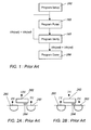
- FIG. 1 A state diagram of prior art for a program operation with program verify is shown in FIG. 1.
- the first program setup 101 is needed to startup the charge pumps and setup the voltages needed for the program operation.
- the selected memory cell is subjected to program voltage conditions during the program pulse step 102.
- the threshold of the memory cell is tested in the program verify step103. If the threshold of the memory cell is greater than the reference threshold, then the memory cell is deemed to have been programmed, and program is complete 104. Otherwise if the threshold of the selected memory cell is not high enough, then the memory cell is placed back into the program state 102.
- FIG. 2a gives an example of voltage conditions of a MONOS memory cell of prior art for program and for program verify of prior art in FIG. 2b.
- the memory cell is composed of a control gate 202, a source 201 and a drain 203. Electrons are stored in the nitride region 204 under the control gate 202. It should be noted that the voltages that are shown are an example only. Actual voltages depend on many specifications such as program speed, oxide thickness, and memory cell dimensions.
- CHE channel hot electron
- program verify is very similar to a read operation, in that one diffusion will be measured with respect to a reference to determine the memory state.
- the control gate 202 is biased to approximately 2V
- the drain 201 is biased to approximately 1V
- the source 203 is biased to 0V.
- the drain 203 is raised to 5V again. This is an inefficient usage of charge, because extra current is needed to raise and lower the drain voltage between program and program verify cycles.
- the transition time between program and program verify increases. This increased transition time increases the overall program operation time.
- FIG. 3 shows a prior art dual storage MONOS memory device (called NROM) in which there are two memory storage sites 304 and 305 within one memory cell, described in US Patent 6,011,725 (Eitan), which is directed to a method of read described called "reverse read".
- the diffusion 303 which is closest to the selected memory storage region 305, becomes the lower voltage or source whereas the diffusion 301, which is opposite the selected memory storage region 305, becomes the higher voltage or drain.
- the drain voltage is higher than the source voltage in order to create a depletion region into the substrate and thus "override" the charge that may be stored in the unselected memory storage region, if it is in the high threshold "0" memory state.
- This type of NROM memory cell can only operate in reverse read mode, because a higher voltage is needed on the unselected memory storage side to override the unselected memory channel. If the device were to be read in the forward direction, then the higher drain voltage would override the selected memory storage side, and the cell would always be sensed to be in a low Vt "1" memory state.
- FIG. 4a Another prior art dual storage MONOS device is described in Patent Application 09/426,692, filed Oct. 25, 1999, called the twin MONOS cell and shown in FIG. 4a.
- this type of memory cell there are two extra side wall polysilicon control gate structures 406 and 407 in addition to the word gate 402 and two diffusions 401 and 403.
- the word gate 402 of FIG. 4a does not have memory nitride storage regions underneath itself. Instead, the memory storage regions lie underneath the side wall polysilicon control gates 406 and 407.
- two side wall polysilicon gates between two adjacent memory cells are electrically connected together to define one equivalent control gate.
- the twin MONOS cell can be easily read in both the reverse and forward directions.
- the channel underneath of the unselected nitride storage site can be overridden by increasing the voltage of the associated control gate to a voltage which is some delta above the highest possible threshold voltage (Vcg override).
- Vcg override the highest possible threshold voltage
- FIG 4b shows the relationship of drain voltage v.s. the threshold of the selected nitride region for memory nitride channel lengths of >50nm and ⁇ 50nm.
- FIG. 4c is a schematic representation of the twin MONOS cell array in the diffusion bit configuration.
- Each memory cell consists of one word gate, two control gate halves, under which each control gate half is one nitride storage region, and two diffusion halves.
- memory cells are arranged in rows and columns, in which word gates are horizontally connected together by word lines WL[0-1], and bit diffusions are vertically connected together by bit lines BL[0-3], and control gates are vertically connected together by control lines CG[0-3].
- Control lines CG[0-3] and bit lines BL[0-3] may run atop of one another and have a coupling capacitance of about 30%.
- a method to produce a fast switch between program and program verify is described for a MONOS memory device.
- the word gate of the cell to be programmed is biased to a low voltage to limit memory cell current to a few microamperes.
- the drain diffusion is biased to a high voltage and the source diffusion is grounded.
- the drain diffusion is the diffusion near the storage site to be programmed in a two storage site device.
- the storage site is a nitride region located below a control gate. In a two storage site device there are two control gates and two separate nitride regions.
- the unselected control gate is biased to a high voltage to override the highest possible threshold voltage of the memory storage region beneath the unselected control gate.
- the selected control gate is the control gate above the storage site to be programmed and is biased to a high voltage for electron injection into the nitride storage site.
- the source diffusion can be connected to a load device to limit and control cell current, and cell current can be controlled with a low word gate voltage.
- To control program disturb of the adjacent cell the voltage of the unselected diffusion of the adjacent cell is increased slightly. Increasing the voltage of the unselected adjacent diffusion decreases the gate to source voltage as well as increases the threshold voltage of the adjacent storage region and protects the cell from program disturb.
- a program verify operation is necessary to determine if the cell being programmed has reach a sufficient program voltage. To do this there is a minimum of one switch from the program operation to a program verify operation and back. There can be several switches between operations during the programming of a cell. If the voltages involved in the two operations are substantially dissimilar, there is considerable charging and discharging of the various connecting lines, which results in time delays. To minimize the time delays between the two operations the bit line voltages and the control gate voltages are made the same as much as possible during both program and program verify. Also one variation of program verify uses a "forward read" direction which puts the lower voltage on the diffusion opposite the selected nitride storage site.
- the "forward read” operation allows minimal charging and discharging of the bit lines and control gates. This forward read approach is most effective when the channel length under the nitride region is long and the threshold voltage reduction as a function of drain-source voltage, shown in FIG. 4b, is small.
- the source and drain bit lines are equalized to a voltage that is half of the high drain voltage during program.
- the selected control gate voltage is lowered slightly, and the word line is then raised to a higher voltage to allow the word gate channel to conduct.
- one of the two bit lines is pulled down to a lower voltage.
- a sense amplifier connected to the bit line monitors the other bit line with respect to a reference voltage; if the target nitride region has been programmed enough, the voltage will be maintained, otherwise it will also fall. Verify can be performed in both the forward and reverse directions by choosing which of the two bit lines to pull down, or connect to the sense amplifier.
- program is performed by utilizing the capacitance of the BL. Due to the high injection efficiency of the channel hot electron (CHE) program for the twin MONOS memory, program can be sufficiently completed within a short time, by using the charge stored on the capacitance of the high voltage drain side bit line.
- Program verify is performed by utilizing capacitance of the BL and the coupling capacitance between the bit lines and the control gate lines in order to increase the threshold voltage range.
- First the appropriate voltages are applied to the control gate lines and bit lines for the program.
- the control gate lines and bit lines are then floated and the word line is raised to a low voltage to limit the program current. When the word line turns on, all channels between the source and drain are on, so that charge will flow between the two bit lines.
- the low voltage of the word line also limits the source bit line voltage.
- injection will stop.
- the word line is raised to a high voltage in order for both bit lines to equalize to a middle voltage. Thereafter, the bit line closest to the selected nitride region will be pulled down to a lower voltage.
- the threshold of the verify operation is determined by the control gate voltage of the selected side minus the lower bit line voltage.
- the voltage of the opposite bit line may be monitored to determine whether the selected nitride region has been programmed enough such that the bit line voltage is maintained, and doesn't fall.
- the program to program verify sequences described in the present invention may also be applied to high program bandwidth applications for storage of multiple threshold levels in a single nitride region.
- the memory cell 410 is comprised of one word gate 402, a left diffusion region 401, a right diffusion region 403, and two control gates 406and 407, and two nitride storage sites 404 and 405.
- the left nitride storage site 404 is positioned under the left control gate 406, above the left diffusion 401, and close to the word gate 402.
- the right nitride storage site 405 is positioned under the right control gate 407, above the right diffusion 403, and close to the word gate 402.
- the program condition shown are significantly lower than the program voltages for a conventional MONOS device.
- the voltage difference is due to the enhanced electron injection mechanism for the twin MONOS device.
- the voltages shown are approximations only. The actual voltages need to be determined based on process and product specification factors such as threshold shift, oxide and ONO thickness, doping profiles, and the program and erase time specifications. It is assumed that the threshold for a "0" state is Vth> 2.0V, the threshold for a "1" state is about 0.5V, and the word gate 503 threshold is 0.5V.
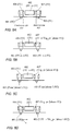
- FIG. 5a shows the voltage conditions of the present invention, when the right nitride storage site is selected.
- an approximate 5V drain to source voltage is applied across the memory cell.
- the diffusion 403 closest to the selected storage site becomes the drain.
- the right diffusion 403 is determined have the high drain voltage of about 5V, and the left diffusion 401 becomes the source, which is around 0V.
- a low word gate voltage of approximately 1V limits program cell current.
- the left control gate 406 is biased to a high voltage of approximately 5V to override a possible high threshold state in the unselected memory storage region 404.
- the higher voltage of 5V is selected to be the same override voltage as used during program verify to reduce the transition time between program and program verify modes.
- the right control gate 407 is biased to 5V.
- FIG. 5b gives the voltage conditions during transition between program and program verify mode.
- the control gate 406 remains near 5V.
- the source diffusion 401 and drain diffusion 403 is equalized to about 2.5V, which is half of the high drain voltage used for program.
- the voltage of the right control gate 407 is changed to Vcg_pv, which is about 4V for a target threshold of 2.0V, when body effect is considered. After the voltages of both the left and right diffusion 401 and 403 have settled to 2.5, both diffusions are floated as shown in FIG. 5c.
- the word gate 402 is then raised to a high voltage of about 4V, in order to allow the diffusion voltages of 2.5V to pass easily. It is also possible to equalize the bit lines at the same time the word line is being raised.
- the final step of the program verify sequence is shown in FIG. 5d.
- the voltage of the right diffusion 403 is pulled down to Vbl_pv, which can be about 1.8V and the voltage of the left diffusion 401 is monitored. If the threshold of the right nitride region 405 is greater than the target 2.0V, then the left diffusion 401 voltage will remain at about 2.5V. Otherwise, if the threshold is lower than 2.0V, the left diffusion 401 voltage will fall.
- the target program threshold voltage is determined by the voltage of Vcg_pv and the Vbl_pv, where Vtarget_threshold ⁇ Vcg_pv - Vbl_pv, considering that the nonzero source-substrate voltage introduces a body effect component to Vtarget_threshold.
- FIG. 6 shows simulation results for the program verify sequence described by FIG. 5a through d for the first embodiment. Shown are voltage curves versus time for the left control gate CGL 406, the right control gate CGR 407, the word gate WL 402, the left bit line BLL 401, and the right bit line BLR 403. The effects of threshold voltage are shown for the left bit line BLL 401.
- program verify can be conducted in the forward read direction.
- the program and verify sequences shown in FIG. 5a through c are the same. However, in the last step, the voltage conditions in FIG. 7 are substituted for those of FIG. 5d.
- the source and drain diffusions swap compared to during reverse read.
- the voltage of the left diffusion 401 farther from the selected nitride 405 is pulled down to a voltage of Vbl_pv.
- the voltage of the right diffusion 403 closer to the selected nitride region 405 is monitored to determine the threshold value. If the selected nitride region 405 threshold is greater than 2.0V, then the right diffusion voltage 403 will be maintained.
- Vcg_pv For forward read, threshold voltage degrades as a function of drain-source voltage, so it is important to keep the drain to source voltage to between 0.3 to 0.5V.
- Vcg_pv In order to verify a target threshold of 2.0V, Vcg_pv should be 2.0V (plus some additional voltage to account for body effect) greater than the Vbl_pv.
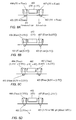
- FIG. 8a through b the sequence for program is given in FIG. 8a through b, and the program verify sequence is shown in FIG. 8c through d.
- FIG. 8a gives the voltage conditions in order to program the right nitride region 405 of the twin MONOS memory cell of FIG. 4a.
- the left control gate 406 is biased to an override voltage of about 5V.
- the right control gate 407 is biased to a selected program voltage of approximately 5V.
- the left diffusion 401 is grounded and the right diffusion 403 is raised to a high drain voltage of approximately 5V.
- the word line which is connected to word gate 402, is then raised and program begins when electrons start to flow from the source bit line to the drain bit line.
- the high CHE injection efficiency of the twin MONOS cell of the present invention allows sufficient programming using the energy stored in the high drain voltage bit line, without actually DC biasing of the source and drain.
- the word line voltage also limits the extent of bit line equalization, because the source bit line will not rise past the voltage of the word line minus the threshold voltage of the word gate, which is approximately 0.5V. Thus, after the source bit line rises to 0.5V, and the drain bit line falls to 4.5V, charge will no longer flow between the two bit lines and so CHE injection will stop. Changes in the bit line voltages also affect the voltages of the two floating control gate lines.
- the bit line and control gate voltages after program has stopped are given in FIG. 8b.
- the word gate 402 voltage is raised to a higher voltage of about 4V in order to equalize the left and right bit lines to a middle voltage of approximately 2.5V and then floated.
- the control gate voltages which are capacitive coupled, such that the left control gate 406 rises to 5.75V and the right control gate 407 falls to 4.25V.
- This voltage of the right control gate 407 is equivalent to the Vcg_pv in the first embodiment of the present invention.
- Vtarget_threshold Vcg_pv - Vbl_pv
- Vcg_pv does not have to be externally applied to the memory cell. Instead, it can be derived by a unique timing sequence and utilizing the capacitive coupling between the bit line and control gate line.
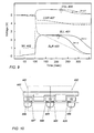
- FIG. 9 shows simulation results for the program verify sequence described by FIG. 8a through d for the third embodiment. Shown are voltage curves versus time for the left control gate CGL 406, the right control gate CGR 407, the word gate WL 402, the left bit line BLL 401, and the right bit line BLR 403. The effects of threshold voltage are shown for the left bit line BLL 401 and the left control gate 406.
- the first and third embodiments of the present invention may be applied to high program bandwidth applications for storage of multiple threshold levels in a single nitride region.
- Vtarget_threshold ⁇ Vcg_pv - Vbl_pv the desired threshold can be tightly controlled.
- body effect due to source-substrate bias needs also needs to be considered
- threshold voltage increments of less than 0.1V can be resolved by setting the values of Vcg_pv or Vbl_pv, or both.
- program verify time can be reduced by setting Vcg_pv - Vbl_pv > Vtarget_threshold. Both the insufficiently programmed bit line and the sufficiently programmed bit line voltages will fall, however it is possible to distinguish between the two cases by comparing the bit line voltage to a reference voltage or reference cell. If the bit line fall remains above the reference voltage within a given time interval, then the cell has been programmed enough.
- FIG. 10 shows a cross-section of two adjacent memory cells 601 and 602.
- the adjacent memory storage region 609 in the adjacent cell 602 sharing the same high voltage control gate and high voltage diffusion 605, is in danger of program disturb.
- the opposite right side memory storage region 610 in the right cell 602 has a negative threshold, it is possible that the adjacent right cell 602 may conduct current, thereby programming the memory storage region 609 of the unselected adjacent cell.
- the unselected adjacent diffusion 606 is biased to a slightly high voltage, approximately 1V. Increasing the voltage of the unselected adjacent diffusion 606 effectively increases the threshold of the memory storage region 610, as well as raises the source voltage of the cell. It is important that this diffusion voltage not be too high, or program disturb may propagate to the adjacent cell of the adjacent cell of 601.
- the current of the memory cell is controlled by connecting a current load transistor to the left source diffusion 401.
Landscapes
- Engineering & Computer Science (AREA)
- Microelectronics & Electronic Packaging (AREA)
- Read Only Memory (AREA)
- Non-Volatile Memory (AREA)
- Semiconductor Memories (AREA)
- Circuits Of Receivers In General (AREA)
- Debugging And Monitoring (AREA)
- Storage Device Security (AREA)
Applications Claiming Priority (2)
| Application Number | Priority Date | Filing Date | Title |
|---|---|---|---|
| US25582400P | 2000-12-15 | 2000-12-15 | |
| US255824P | 2000-12-15 |
Publications (3)
| Publication Number | Publication Date |
|---|---|
| EP1215680A2 true EP1215680A2 (fr) | 2002-06-19 |
| EP1215680A3 EP1215680A3 (fr) | 2004-01-21 |
| EP1215680B1 EP1215680B1 (fr) | 2008-03-19 |
Family
ID=22970026
Family Applications (1)
| Application Number | Title | Priority Date | Filing Date |
|---|---|---|---|
| EP01480133A Expired - Lifetime EP1215680B1 (fr) | 2000-12-15 | 2001-12-14 | Procédé rapide de programmation et de vérification de programmation |
Country Status (7)
| Country | Link |
|---|---|
| US (8) | US6549463B2 (fr) |
| EP (1) | EP1215680B1 (fr) |
| JP (1) | JP4050048B2 (fr) |
| KR (1) | KR100880547B1 (fr) |
| AT (1) | ATE389937T1 (fr) |
| DE (1) | DE60133259D1 (fr) |
| TW (1) | TW577082B (fr) |
Cited By (2)
| Publication number | Priority date | Publication date | Assignee | Title |
|---|---|---|---|---|
| KR100880547B1 (ko) * | 2000-12-15 | 2009-01-30 | 헤이로 엘에스아이 디자인 앤드 디바이스 테크놀로지 인크 | 메모리 셀 프로그래밍 방법 및 프로그램 검증 방법 |
| CN100543875C (zh) * | 2004-09-01 | 2009-09-23 | 旺宏电子股份有限公司 | 非易失存储器的编程方法 |
Families Citing this family (32)
| Publication number | Priority date | Publication date | Assignee | Title |
|---|---|---|---|---|
| JP4084922B2 (ja) * | 2000-12-22 | 2008-04-30 | 株式会社ルネサステクノロジ | 不揮発性記憶装置の書込み方法 |
| WO2002097821A1 (fr) * | 2001-05-25 | 2002-12-05 | Fujitsu Limited | Dispositif de stockage non volatile a semi-conducteur |
| JP2003151290A (ja) * | 2001-07-06 | 2003-05-23 | Halo Lsi Inc | コントロール・ゲート及びワード線電圧の昇圧回路 |
| US6925007B2 (en) * | 2001-10-31 | 2005-08-02 | Sandisk Corporation | Multi-state non-volatile integrated circuit memory systems that employ dielectric storage elements |
| US6897522B2 (en) * | 2001-10-31 | 2005-05-24 | Sandisk Corporation | Multi-state non-volatile integrated circuit memory systems that employ dielectric storage elements |
| US6795349B2 (en) * | 2002-02-28 | 2004-09-21 | Sandisk Corporation | Method and system for efficiently reading and programming of dual cell memory elements |
| JP3900979B2 (ja) * | 2002-03-14 | 2007-04-04 | セイコーエプソン株式会社 | 不揮発性レジスタおよび半導体装置 |
| US6747893B2 (en) * | 2002-03-14 | 2004-06-08 | Intel Corporation | Storing data in non-volatile memory devices |
| JP3843869B2 (ja) * | 2002-03-15 | 2006-11-08 | セイコーエプソン株式会社 | 不揮発性半導体記憶装置 |
| US6888755B2 (en) * | 2002-10-28 | 2005-05-03 | Sandisk Corporation | Flash memory cell arrays having dual control gates per memory cell charge storage element |
| US7031192B1 (en) | 2002-11-08 | 2006-04-18 | Halo Lsi, Inc. | Non-volatile semiconductor memory and driving method |
| JP2004348792A (ja) * | 2003-05-20 | 2004-12-09 | Sharp Corp | 半導体記憶装置、表示装置及び携帯電子機器 |
| US6992917B2 (en) * | 2003-12-15 | 2006-01-31 | International Business Machines Corporation | Integrated circuit with reduced body effect sensitivity |
| US20050251617A1 (en) * | 2004-05-07 | 2005-11-10 | Sinclair Alan W | Hybrid non-volatile memory system |
| US7206224B1 (en) * | 2004-04-16 | 2007-04-17 | Spansion Llc | Methods and systems for high write performance in multi-bit flash memory devices |
| WO2005109438A2 (fr) * | 2004-05-06 | 2005-11-17 | Halo Lsi, Inc. | Operations dynamiques de memoire remanente |
| JP4422556B2 (ja) * | 2004-06-10 | 2010-02-24 | 株式会社ルネサステクノロジ | 不揮発性半導体記憶装置およびその書き込み方法 |
| US7145372B2 (en) * | 2004-08-31 | 2006-12-05 | Micron Technology, Inc. | Startup circuit and method |
| JP2006278987A (ja) | 2005-03-30 | 2006-10-12 | Nec Electronics Corp | 不揮発性記憶素子およびその製造方法 |
| US7180779B2 (en) * | 2005-07-11 | 2007-02-20 | Atmel Corporation | Memory architecture with enhanced over-erase tolerant control gate scheme |
| US7388252B2 (en) * | 2005-09-23 | 2008-06-17 | Macronix International Co., Ltd. | Two-bits per cell not-and-gate (NAND) nitride trap memory |
| US7951669B2 (en) * | 2006-04-13 | 2011-05-31 | Sandisk Corporation | Methods of making flash memory cell arrays having dual control gates per memory cell charge storage element |
| JP2009076188A (ja) * | 2007-08-24 | 2009-04-09 | Renesas Technology Corp | 不揮発性半導体記憶装置 |
| US7808833B2 (en) * | 2008-01-28 | 2010-10-05 | Qimonda Flash Gmbh | Method of operating an integrated circuit, integrated circuit and method to determine an operating point |
| CN101968972B (zh) * | 2010-07-23 | 2016-04-13 | 上海华虹宏力半导体制造有限公司 | 分裂栅快闪存储单元的编程验证方法 |
| CN101986389B (zh) * | 2010-10-12 | 2015-06-24 | 上海华虹宏力半导体制造有限公司 | 闪存单元、闪存装置及其编程方法 |
| US9098553B2 (en) | 2013-03-15 | 2015-08-04 | Gridglo Llc | System and method for remote activity detection |
| US9082490B2 (en) * | 2013-06-18 | 2015-07-14 | Flashsilicon Incorporation | Ultra-low power programming method for N-channel semiconductor non-volatile memory |
| TWI627636B (zh) * | 2017-05-23 | 2018-06-21 | 旺宏電子股份有限公司 | 感測放大器以及用於其位元線電壓補償的方法 |
| US11507816B2 (en) * | 2019-09-19 | 2022-11-22 | Silicon Storage Technology, Inc. | Precision tuning for the programming of analog neural memory in a deep learning artificial neural network |
| CN113129940B (zh) * | 2019-12-30 | 2025-02-07 | 兆易创新科技集团股份有限公司 | 一种闪存及其制造方法 |
| EP4047802A1 (fr) * | 2021-02-17 | 2022-08-24 | Schaffner EMV AG | Filtre actif anti-interférences électromagnétiques |
Family Cites Families (43)
| Publication number | Priority date | Publication date | Assignee | Title |
|---|---|---|---|---|
| BR8807352A (pt) | 1987-02-13 | 1990-03-01 | Dow Chemical Co | Metodo para fabricar dispositivo de armazenamento de memoria otica e dispositivo de armazenamento otico |
| US5784327A (en) * | 1991-06-12 | 1998-07-21 | Hazani; Emanuel | Memory cell array selection circuits |
| US5357462A (en) * | 1991-09-24 | 1994-10-18 | Kabushiki Kaisha Toshiba | Electrically erasable and programmable non-volatile semiconductor memory with automatic write-verify controller |
| US7071060B1 (en) * | 1996-02-28 | 2006-07-04 | Sandisk Corporation | EEPROM with split gate source side infection with sidewall spacers |
| US5712180A (en) * | 1992-01-14 | 1998-01-27 | Sundisk Corporation | EEPROM with split gate source side injection |
| US6222762B1 (en) * | 1992-01-14 | 2001-04-24 | Sandisk Corporation | Multi-state memory |
| US5592415A (en) * | 1992-07-06 | 1997-01-07 | Hitachi, Ltd. | Non-volatile semiconductor memory |
| JP2541087B2 (ja) * | 1992-10-30 | 1996-10-09 | 日本電気株式会社 | 不揮発性半導体記憶装置のデ―タ消去方法 |
| JP3252306B2 (ja) * | 1993-08-10 | 2002-02-04 | 株式会社日立製作所 | 半導体不揮発性記憶装置 |
| US5467308A (en) * | 1994-04-05 | 1995-11-14 | Motorola Inc. | Cross-point eeprom memory array |
| US5422504A (en) * | 1994-05-02 | 1995-06-06 | Motorola Inc. | EEPROM memory device having a sidewall spacer floating gate electrode and process |
| DE19523775C2 (de) * | 1994-06-29 | 2001-12-06 | Toshiba Kawasaki Kk | Nichtflüchtige Halbleiterspeichervorrichtung |
| US5694356A (en) * | 1994-11-02 | 1997-12-02 | Invoice Technology, Inc. | High resolution analog storage EPROM and flash EPROM |
| US5541130A (en) * | 1995-06-07 | 1996-07-30 | International Business Machines Corporation | Process for making and programming a flash memory array |
| JP3517489B2 (ja) * | 1995-09-04 | 2004-04-12 | 株式会社日立製作所 | 不揮発性半導体記憶装置 |
| JP3184082B2 (ja) * | 1995-11-24 | 2001-07-09 | 日本電気株式会社 | 不揮発性半導体記憶装置 |
| US5712815A (en) * | 1996-04-22 | 1998-01-27 | Advanced Micro Devices, Inc. | Multiple bits per-cell flash EEPROM capable of concurrently programming and verifying memory cells and reference cells |
| JP3404712B2 (ja) * | 1996-05-15 | 2003-05-12 | 株式会社東芝 | 不揮発性半導体記憶装置及びその書き込み方法 |
| US5748538A (en) * | 1996-06-17 | 1998-05-05 | Aplus Integrated Circuits, Inc. | OR-plane memory cell array for flash memory with bit-based write capability, and methods for programming and erasing the memory cell array |
| TW367503B (en) * | 1996-11-29 | 1999-08-21 | Sanyo Electric Co | Non-volatile semiconductor device |
| JP3481817B2 (ja) * | 1997-04-07 | 2003-12-22 | 株式会社東芝 | 半導体記憶装置 |
| US5889303A (en) * | 1997-04-07 | 1999-03-30 | Motorola, Inc. | Split-Control gate electrically erasable programmable read only memory (EEPROM) cell |
| US6031760A (en) * | 1997-07-29 | 2000-02-29 | Kabushiki Kaisha Toshiba | Semiconductor memory device and method of programming the same |
| IL125604A (en) * | 1997-07-30 | 2004-03-28 | Saifun Semiconductors Ltd | Non-volatile electrically erasable and programmble semiconductor memory cell utilizing asymmetrical charge |
| US6768165B1 (en) | 1997-08-01 | 2004-07-27 | Saifun Semiconductors Ltd. | Two bit non-volatile electrically erasable and programmable semiconductor memory cell utilizing asymmetrical charge trapping |
| US6108238A (en) * | 1997-09-11 | 2000-08-22 | Kabushiki Kaisha Toshiba | Programmable semiconductor memory device having program voltages and verify voltages |
| KR100287885B1 (ko) * | 1997-12-31 | 2001-05-02 | 김영환 | 반도체 메모리 장치 |
| KR100327421B1 (ko) * | 1997-12-31 | 2002-07-27 | 주식회사 하이닉스반도체 | 비휘발성 메모리 소자의 프로그램 시스템 및 그의 프로그램 방법 |
| US6353242B1 (en) * | 1998-03-30 | 2002-03-05 | Kabushiki Kaisha Toshiba | Nonvolatile semiconductor memory |
| JPH11317085A (ja) * | 1998-05-08 | 1999-11-16 | Sony Corp | プログラム・ベリファイ回路及びプログラム・ベリファイ方法 |
| US6208542B1 (en) * | 1998-06-30 | 2001-03-27 | Sandisk Corporation | Techniques for storing digital data in an analog or multilevel memory |
| US6180461B1 (en) * | 1998-08-03 | 2001-01-30 | Halo Lsi Design & Device Technology, Inc. | Double sidewall short channel split gate flash memory |
| JP2000138300A (ja) * | 1998-10-30 | 2000-05-16 | Sony Corp | 不揮発性半導体記憶装置及びその書き込み方法 |
| US6975539B2 (en) * | 1999-01-14 | 2005-12-13 | Silicon Storage Technology, Inc. | Digital multilevel non-volatile memory system |
| US7031214B2 (en) * | 1999-01-14 | 2006-04-18 | Silicon Storage Technology, Inc. | Digital multilevel memory system having multistage autozero sensing |
| US6133098A (en) * | 1999-05-17 | 2000-10-17 | Halo Lsi Design & Device Technology, Inc. | Process for making and programming and operating a dual-bit multi-level ballistic flash memory |
| US6248633B1 (en) | 1999-10-25 | 2001-06-19 | Halo Lsi Design & Device Technology, Inc. | Process for making and programming and operating a dual-bit multi-level ballistic MONOS memory |
| US6490204B2 (en) * | 2000-05-04 | 2002-12-03 | Saifun Semiconductors Ltd. | Programming and erasing methods for a reference cell of an NROM array |
| US6292394B1 (en) * | 2000-06-29 | 2001-09-18 | Saifun Semiconductors Ltd. | Method for programming of a semiconductor memory cell |
| TW503528B (en) * | 2000-07-12 | 2002-09-21 | Koninkl Philips Electronics Nv | Semiconductor device |
| JP2002170891A (ja) * | 2000-11-21 | 2002-06-14 | Halo Lsi Design & Device Technol Inc | デュアルビット多準位バリスティックmonosメモリの製造、プログラミング、および動作のプロセス |
| DE60133619T2 (de) * | 2000-12-05 | 2009-06-10 | Halo Lsi Design And Device Technology Inc. | Programmier- und Löschverfahren in Zwilling-MONOS-Zellenspeichern |
| DE60133259D1 (de) * | 2000-12-15 | 2008-04-30 | Halo Lsi Design & Device Tech | Schnelles Programmier- und Programmierverifikationsverfahren |
-
2001
- 2001-12-14 DE DE60133259T patent/DE60133259D1/de not_active Expired - Lifetime
- 2001-12-14 AT AT01480133T patent/ATE389937T1/de not_active IP Right Cessation
- 2001-12-14 EP EP01480133A patent/EP1215680B1/fr not_active Expired - Lifetime
- 2001-12-14 TW TW090131003A patent/TW577082B/zh not_active IP Right Cessation
- 2001-12-14 US US10/016,916 patent/US6549463B2/en not_active Expired - Lifetime
- 2001-12-14 JP JP2001381765A patent/JP4050048B2/ja not_active Expired - Lifetime
- 2001-12-15 KR KR1020010079717A patent/KR100880547B1/ko not_active Expired - Fee Related
-
2003
- 2003-02-20 US US10/371,836 patent/US6628546B2/en not_active Expired - Fee Related
- 2003-02-20 US US10/371,514 patent/US6611461B2/en not_active Expired - Lifetime
- 2003-02-20 US US10/371,520 patent/US6856545B2/en not_active Expired - Lifetime
- 2003-02-20 US US10/371,839 patent/US6628547B2/en not_active Expired - Lifetime
- 2003-02-20 US US10/371,518 patent/US7046553B2/en not_active Expired - Lifetime
- 2003-02-20 US US10/371,519 patent/US6807105B2/en not_active Expired - Lifetime
- 2003-02-20 US US10/371,840 patent/US6636439B1/en not_active Expired - Lifetime
Cited By (2)
| Publication number | Priority date | Publication date | Assignee | Title |
|---|---|---|---|---|
| KR100880547B1 (ko) * | 2000-12-15 | 2009-01-30 | 헤이로 엘에스아이 디자인 앤드 디바이스 테크놀로지 인크 | 메모리 셀 프로그래밍 방법 및 프로그램 검증 방법 |
| CN100543875C (zh) * | 2004-09-01 | 2009-09-23 | 旺宏电子股份有限公司 | 非易失存储器的编程方法 |
Also Published As
| Publication number | Publication date |
|---|---|
| US6636439B1 (en) | 2003-10-21 |
| US20020075725A1 (en) | 2002-06-20 |
| ATE389937T1 (de) | 2008-04-15 |
| JP4050048B2 (ja) | 2008-02-20 |
| US6856545B2 (en) | 2005-02-15 |
| US20030123293A1 (en) | 2003-07-03 |
| US20030185053A1 (en) | 2003-10-02 |
| US6628546B2 (en) | 2003-09-30 |
| US20030123292A1 (en) | 2003-07-03 |
| EP1215680A3 (fr) | 2004-01-21 |
| US20030128588A1 (en) | 2003-07-10 |
| KR20020071442A (ko) | 2002-09-12 |
| EP1215680B1 (fr) | 2008-03-19 |
| US6549463B2 (en) | 2003-04-15 |
| US7046553B2 (en) | 2006-05-16 |
| US6628547B2 (en) | 2003-09-30 |
| US20030123308A1 (en) | 2003-07-03 |
| US6807105B2 (en) | 2004-10-19 |
| DE60133259D1 (de) | 2008-04-30 |
| US20030123290A1 (en) | 2003-07-03 |
| US6611461B2 (en) | 2003-08-26 |
| TW577082B (en) | 2004-02-21 |
| JP2002230988A (ja) | 2002-08-16 |
| KR100880547B1 (ko) | 2009-01-30 |
| US20030123291A1 (en) | 2003-07-03 |
Similar Documents
| Publication | Publication Date | Title |
|---|---|---|
| US6611461B2 (en) | Fast program to program verify method | |
| US8027202B2 (en) | Method of programming a flash memory device using self boosting | |
| US7929344B2 (en) | Semiconductor memory device having stacked gate including charge accumulation layer and control gate | |
| US8000150B2 (en) | Method of programming memory device | |
| US6459622B1 (en) | Twin MONOS memory cell usage for wide program | |
| US7839696B2 (en) | Method of programming and erasing a p-channel BE-SONOS NAND flash memory | |
| TWI331757B (en) | Self-boosting method for flash memory cells | |
| US20040174748A1 (en) | Self boosting technique | |
| US7787294B2 (en) | Operating method of memory | |
| US7839694B2 (en) | Nonvolatile memory devices and data reading methods | |
| US7272043B2 (en) | Operation methods for a non-volatile memory cell in an array | |
| KR100861749B1 (ko) | 2t nor형 비휘발성 메모리 셀 어레이, 2t nor형비휘발성 메모리의 데이터 처리방법 | |
| US7342833B2 (en) | Nonvolatile memory cell programming | |
| US7778081B2 (en) | Method for performing operations by applying periodic voltage pulses to control gate of an ono memory cell | |
| US7301820B2 (en) | Non-volatile memory dynamic operations | |
| US7054192B2 (en) | Method of controlling threshold voltage of NROM cell | |
| KR0170710B1 (ko) | 불휘발성 반도체 메모리 장치 |
Legal Events
| Date | Code | Title | Description |
|---|---|---|---|
| PUAI | Public reference made under article 153(3) epc to a published international application that has entered the european phase |
Free format text: ORIGINAL CODE: 0009012 |
|
| AK | Designated contracting states |
Kind code of ref document: A2 Designated state(s): AT BE CH CY DE DK ES FI FR GB GR IE IT LI LU MC NL PT SE TR |
|
| AX | Request for extension of the european patent |
Free format text: AL;LT;LV;MK;RO;SI |
|
| PUAL | Search report despatched |
Free format text: ORIGINAL CODE: 0009013 |
|
| AK | Designated contracting states |
Kind code of ref document: A3 Designated state(s): AT BE CH CY DE DK ES FI FR GB GR IE IT LI LU MC NL PT SE TR |
|
| AX | Request for extension of the european patent |
Extension state: AL LT LV MK RO SI |
|
| RIC1 | Information provided on ipc code assigned before grant |
Ipc: 7G 11C 16/14 B Ipc: 7G 11C 16/10 A Ipc: 7G 11C 16/34 B |
|
| 17P | Request for examination filed |
Effective date: 20040721 |
|
| 17Q | First examination report despatched |
Effective date: 20040826 |
|
| AKX | Designation fees paid |
Designated state(s): AT BE CH CY DE DK ES FI FR GB GR IE IT LI LU MC NL PT SE TR |
|
| 17Q | First examination report despatched |
Effective date: 20040826 |
|
| GRAP | Despatch of communication of intention to grant a patent |
Free format text: ORIGINAL CODE: EPIDOSNIGR1 |
|
| GRAS | Grant fee paid |
Free format text: ORIGINAL CODE: EPIDOSNIGR3 |
|
| GRAA | (expected) grant |
Free format text: ORIGINAL CODE: 0009210 |
|
| AK | Designated contracting states |
Kind code of ref document: B1 Designated state(s): AT BE CH CY DE DK ES FI FR GB GR IE IT LI LU MC NL PT SE TR |
|
| REG | Reference to a national code |
Ref country code: GB Ref legal event code: FG4D |
|
| REG | Reference to a national code |
Ref country code: CH Ref legal event code: EP |
|
| REF | Corresponds to: |
Ref document number: 60133259 Country of ref document: DE Date of ref document: 20080430 Kind code of ref document: P |
|
| REG | Reference to a national code |
Ref country code: IE Ref legal event code: FG4D |
|
| PG25 | Lapsed in a contracting state [announced via postgrant information from national office to epo] |
Ref country code: FI Free format text: LAPSE BECAUSE OF FAILURE TO SUBMIT A TRANSLATION OF THE DESCRIPTION OR TO PAY THE FEE WITHIN THE PRESCRIBED TIME-LIMIT Effective date: 20080319 |
|
| PG25 | Lapsed in a contracting state [announced via postgrant information from national office to epo] |
Ref country code: AT Free format text: LAPSE BECAUSE OF FAILURE TO SUBMIT A TRANSLATION OF THE DESCRIPTION OR TO PAY THE FEE WITHIN THE PRESCRIBED TIME-LIMIT Effective date: 20080319 |
|
| NLV1 | Nl: lapsed or annulled due to failure to fulfill the requirements of art. 29p and 29m of the patents act | ||
| PG25 | Lapsed in a contracting state [announced via postgrant information from national office to epo] |
Ref country code: BE Free format text: LAPSE BECAUSE OF FAILURE TO SUBMIT A TRANSLATION OF THE DESCRIPTION OR TO PAY THE FEE WITHIN THE PRESCRIBED TIME-LIMIT Effective date: 20080319 |
|
| PG25 | Lapsed in a contracting state [announced via postgrant information from national office to epo] |
Ref country code: SE Free format text: LAPSE BECAUSE OF FAILURE TO SUBMIT A TRANSLATION OF THE DESCRIPTION OR TO PAY THE FEE WITHIN THE PRESCRIBED TIME-LIMIT Effective date: 20080619 Ref country code: PT Free format text: LAPSE BECAUSE OF FAILURE TO SUBMIT A TRANSLATION OF THE DESCRIPTION OR TO PAY THE FEE WITHIN THE PRESCRIBED TIME-LIMIT Effective date: 20080826 Ref country code: ES Free format text: LAPSE BECAUSE OF FAILURE TO SUBMIT A TRANSLATION OF THE DESCRIPTION OR TO PAY THE FEE WITHIN THE PRESCRIBED TIME-LIMIT Effective date: 20080630 |
|
| PG25 | Lapsed in a contracting state [announced via postgrant information from national office to epo] |
Ref country code: NL Free format text: LAPSE BECAUSE OF FAILURE TO SUBMIT A TRANSLATION OF THE DESCRIPTION OR TO PAY THE FEE WITHIN THE PRESCRIBED TIME-LIMIT Effective date: 20080319 |
|
| ET | Fr: translation filed | ||
| PLBE | No opposition filed within time limit |
Free format text: ORIGINAL CODE: 0009261 |
|
| STAA | Information on the status of an ep patent application or granted ep patent |
Free format text: STATUS: NO OPPOSITION FILED WITHIN TIME LIMIT |
|
| PG25 | Lapsed in a contracting state [announced via postgrant information from national office to epo] |
Ref country code: DK Free format text: LAPSE BECAUSE OF FAILURE TO SUBMIT A TRANSLATION OF THE DESCRIPTION OR TO PAY THE FEE WITHIN THE PRESCRIBED TIME-LIMIT Effective date: 20080319 Ref country code: DE Free format text: LAPSE BECAUSE OF FAILURE TO SUBMIT A TRANSLATION OF THE DESCRIPTION OR TO PAY THE FEE WITHIN THE PRESCRIBED TIME-LIMIT Effective date: 20080620 |
|
| 26N | No opposition filed |
Effective date: 20081222 |
|
| PG25 | Lapsed in a contracting state [announced via postgrant information from national office to epo] |
Ref country code: MC Free format text: LAPSE BECAUSE OF NON-PAYMENT OF DUE FEES Effective date: 20081231 |
|
| REG | Reference to a national code |
Ref country code: CH Ref legal event code: PL |
|
| GBPC | Gb: european patent ceased through non-payment of renewal fee |
Effective date: 20081214 |
|
| PG25 | Lapsed in a contracting state [announced via postgrant information from national office to epo] |
Ref country code: IT Free format text: LAPSE BECAUSE OF FAILURE TO SUBMIT A TRANSLATION OF THE DESCRIPTION OR TO PAY THE FEE WITHIN THE PRESCRIBED TIME-LIMIT Effective date: 20080319 |
|
| PG25 | Lapsed in a contracting state [announced via postgrant information from national office to epo] |
Ref country code: CY Free format text: LAPSE BECAUSE OF FAILURE TO SUBMIT A TRANSLATION OF THE DESCRIPTION OR TO PAY THE FEE WITHIN THE PRESCRIBED TIME-LIMIT Effective date: 20080319 |
|
| REG | Reference to a national code |
Ref country code: FR Ref legal event code: ST Effective date: 20090831 |
|
| PG25 | Lapsed in a contracting state [announced via postgrant information from national office to epo] |
Ref country code: CH Free format text: LAPSE BECAUSE OF NON-PAYMENT OF DUE FEES Effective date: 20081231 Ref country code: LI Free format text: LAPSE BECAUSE OF NON-PAYMENT OF DUE FEES Effective date: 20081231 Ref country code: IE Free format text: LAPSE BECAUSE OF NON-PAYMENT OF DUE FEES Effective date: 20081215 |
|
| PG25 | Lapsed in a contracting state [announced via postgrant information from national office to epo] |
Ref country code: GB Free format text: LAPSE BECAUSE OF NON-PAYMENT OF DUE FEES Effective date: 20081214 |
|
| PG25 | Lapsed in a contracting state [announced via postgrant information from national office to epo] |
Ref country code: FR Free format text: LAPSE BECAUSE OF NON-PAYMENT OF DUE FEES Effective date: 20081231 |
|
| PG25 | Lapsed in a contracting state [announced via postgrant information from national office to epo] |
Ref country code: LU Free format text: LAPSE BECAUSE OF NON-PAYMENT OF DUE FEES Effective date: 20081214 |
|
| PG25 | Lapsed in a contracting state [announced via postgrant information from national office to epo] |
Ref country code: TR Free format text: LAPSE BECAUSE OF FAILURE TO SUBMIT A TRANSLATION OF THE DESCRIPTION OR TO PAY THE FEE WITHIN THE PRESCRIBED TIME-LIMIT Effective date: 20080319 |
|
| PG25 | Lapsed in a contracting state [announced via postgrant information from national office to epo] |
Ref country code: GR Free format text: LAPSE BECAUSE OF FAILURE TO SUBMIT A TRANSLATION OF THE DESCRIPTION OR TO PAY THE FEE WITHIN THE PRESCRIBED TIME-LIMIT Effective date: 20080620 |