EP1215698A2 - Plasmabildschirm mit Leuchtstoffschicht - Google Patents
Plasmabildschirm mit Leuchtstoffschicht Download PDFInfo
- Publication number
- EP1215698A2 EP1215698A2 EP01000719A EP01000719A EP1215698A2 EP 1215698 A2 EP1215698 A2 EP 1215698A2 EP 01000719 A EP01000719 A EP 01000719A EP 01000719 A EP01000719 A EP 01000719A EP 1215698 A2 EP1215698 A2 EP 1215698A2
- Authority
- EP
- European Patent Office
- Prior art keywords
- phosphor
- color
- phosphors
- plasma
- plasma display
- Prior art date
- Legal status (The legal status is an assumption and is not a legal conclusion. Google has not performed a legal analysis and makes no representation as to the accuracy of the status listed.)
- Granted
Links
Images

Classifications
-
- C—CHEMISTRY; METALLURGY
- C09—DYES; PAINTS; POLISHES; NATURAL RESINS; ADHESIVES; COMPOSITIONS NOT OTHERWISE PROVIDED FOR; APPLICATIONS OF MATERIALS NOT OTHERWISE PROVIDED FOR
- C09K—MATERIALS FOR MISCELLANEOUS APPLICATIONS, NOT PROVIDED FOR ELSEWHERE
- C09K11/00—Luminescent materials, e.g. electroluminescent or chemiluminescent
- C09K11/08—Luminescent materials, e.g. electroluminescent or chemiluminescent containing inorganic luminescent materials
- C09K11/77—Luminescent materials, e.g. electroluminescent or chemiluminescent containing inorganic luminescent materials containing rare earth metals
- C09K11/7728—Luminescent materials, e.g. electroluminescent or chemiluminescent containing inorganic luminescent materials containing rare earth metals containing europium
- C09K11/7734—Aluminates
-
- C—CHEMISTRY; METALLURGY
- C09—DYES; PAINTS; POLISHES; NATURAL RESINS; ADHESIVES; COMPOSITIONS NOT OTHERWISE PROVIDED FOR; APPLICATIONS OF MATERIALS NOT OTHERWISE PROVIDED FOR
- C09K—MATERIALS FOR MISCELLANEOUS APPLICATIONS, NOT PROVIDED FOR ELSEWHERE
- C09K11/00—Luminescent materials, e.g. electroluminescent or chemiluminescent
- C09K11/08—Luminescent materials, e.g. electroluminescent or chemiluminescent containing inorganic luminescent materials
- C09K11/77—Luminescent materials, e.g. electroluminescent or chemiluminescent containing inorganic luminescent materials containing rare earth metals
- C09K11/7715—Luminescent materials, e.g. electroluminescent or chemiluminescent containing inorganic luminescent materials containing rare earth metals containing cerium
- C09K11/7726—Borates
-
- C—CHEMISTRY; METALLURGY
- C09—DYES; PAINTS; POLISHES; NATURAL RESINS; ADHESIVES; COMPOSITIONS NOT OTHERWISE PROVIDED FOR; APPLICATIONS OF MATERIALS NOT OTHERWISE PROVIDED FOR
- C09K—MATERIALS FOR MISCELLANEOUS APPLICATIONS, NOT PROVIDED FOR ELSEWHERE
- C09K11/00—Luminescent materials, e.g. electroluminescent or chemiluminescent
- C09K11/08—Luminescent materials, e.g. electroluminescent or chemiluminescent containing inorganic luminescent materials
- C09K11/77—Luminescent materials, e.g. electroluminescent or chemiluminescent containing inorganic luminescent materials containing rare earth metals
- C09K11/7766—Luminescent materials, e.g. electroluminescent or chemiluminescent containing inorganic luminescent materials containing rare earth metals containing two or more rare earth metals
- C09K11/778—Borates
-
- H—ELECTRICITY
- H01—ELECTRIC ELEMENTS
- H01J—ELECTRIC DISCHARGE TUBES OR DISCHARGE LAMPS
- H01J11/00—Gas-filled discharge tubes with alternating current induction of the discharge, e.g. alternating current plasma display panels [AC-PDP]; Gas-filled discharge tubes without any main electrode inside the vessel; Gas-filled discharge tubes with at least one main electrode outside the vessel
- H01J11/20—Constructional details
- H01J11/34—Vessels, containers or parts thereof, e.g. substrates
- H01J11/42—Fluorescent layers
-
- H—ELECTRICITY
- H01—ELECTRIC ELEMENTS
- H01J—ELECTRIC DISCHARGE TUBES OR DISCHARGE LAMPS
- H01J2211/00—Plasma display panels with alternate current induction of the discharge, e.g. AC-PDPs
- H01J2211/20—Constructional details
- H01J2211/34—Vessels, containers or parts thereof, e.g. substrates
- H01J2211/42—Fluorescent layers
Definitions
- the invention relates to a plasma screen equipped with a front panel, the one Glass plate on which a dielectric layer and a protective layer are applied, with a carrier plate equipped with a fluorescent layer, with a rib structure, the space between the front plate and the carrier plate in plasma cells, which with are filled with a gas, split, and with one or more electrode arrays on the Front plate and the carrier plate for generating silent electrical discharges in the plasma cells.
- Plasma screens allow color images with high resolution, large screen diagonal and are of compact design.
- a plasma screen has a hermetic closed glass cell, which is filled with a gas, arranged with a grid Electrodes on. Applying an electrical voltage causes a gas discharge that produces light in the ultraviolet range. This can be done with phosphors Converted light into visible light and through the front plate of the glass cell Viewers are emitted.
- BaMgAl 10 O 17 : Eu (BAM) is mostly used as a blue phosphor
- Zn 2 SiO 4 Mn (ZSM) as a green phosphor
- (Y, Gd) BO 3 Eu (YGB) as a red phosphor.
- the selection of these phosphors was made mainly with regard to their luminous efficacy when excited with VUV light and their color points.
- the color points of the phosphors used play an enormous role in emissive screens, since they determine the maximum accessible color space.
- each of the selected phosphors has certain disadvantages that cannot be easily remedied.
- the blue fluorescent BaMgAl 10 O 17 : Eu shows a sharp decrease in brightness due to the irradiation with VUV light.
- the white point of the plasma screen shifts in the direction of yellow-orange, since the green and especially the red phosphor degrades less.
- the green phosphor Zn 2 SiO 4 : Mn has a relatively long decay time of about 10 ms and only a moderate efficiency when excited with VUV light. Efficiency continues to decrease significantly with increasing luminance due to saturation. In addition, its stability when excited with VUV light is also lower than that of the red phosphor (Y, Gd) BO 3 : Eu.
- the red phosphor (Y, Gd) BO 3 : Eu is very efficient when excited with VUV light, but its color point is less red than that of Y 2 O 2 S: Eu, which is used in cathode ray tubes.
- the phosphors are provided with a coating, for example, or alternative phosphors are synthesized.
- DE 197 27 607 discloses a blue-emitting aluminate phosphor with a coating of catena polyphosphate of one or more alkaline earth metals, zinc, cadmium and / or manganese.
- the coating of catena polyphosphate reduces the degradation of the phosphor by excitation with VUV light.
- a plasma screen equipped with a front plate which is a glass plate on which a dielectric layer and a protective layer are applied are equipped with a carrier plate with a phosphor layer, the one heterogeneous mixture of at least two phosphors contains the same color emit, with a ribbed structure, the space between the front panel and carrier plate divided into plasma cells filled with a gas, and with one or more Electrode arrays on the front plate and the carrier plate for the production of breastfeeding electrical discharges in the plasma cells.
- the phosphor layer is divided into different color segments and at least one color segment is a heterogeneous mixture of at least two phosphors, that emit the same color.
- the phosphor layer of a plasma display screen usually contains different color segments each with a phosphor, which is in one of the colors blue, green or red emitted. By using two different phosphors, the same Emitting color in a color segment can change the properties of that color segment be improved.
- a color segment of the phosphor layer contains a heterogeneous mixture of BaMgAl 10 O 17 : Eu and a phosphor selected from the group of Ce 3+ -activated phosphors and Tm 3+ -activated phosphors.
- the decrease in the brightness of a blue-emitting phosphor layer or a blue-emitting color segment of a phosphor layer during the life of a plasma display can be reduced, since Ce 3+ -activated phosphors and Tm 3+ -activated phosphors have a higher stability than BaMgAl 10 O 17 : Eu exposed to VUV light.
- the Ce 3+ -activated phosphor is selected from the group YBO 3 : Ce and (Y 1-x Gd x ) BO 3 : Ce with 0 x x 1 1.
- the Tm 3+ activated phosphor is LaBO 3 : Tm.
- a blue-emitting color segment of a phosphor layer can be improved, since YBO 3 : Ce, (Y 1-x Gd x ) BO 3 : Ce with 0 ⁇ x ⁇ 1 and LaBO 3 : Tm have a deeper blue emission color than BaMgAl 10 O 17 : Eu. It is further preferred that a color segment of the phosphor layer contains a heterogeneous mixture of Zn 2 SiO 4 : Mn and a Tb 3+ -activated phosphor.
- the decrease in the brightness of a green-emitting color segment of a phosphor layer during the life of a plasma display can be reduced because Tb 3+ activated phosphors have a higher stability than Zn 2 SiO 4 : Mn when irradiated with VUV light. Because Tb 3+ is relatively difficult to oxidize to Tb 4+ , while Mn 2+ is very sensitive to oxidation. Furthermore, the light yield, in particular in the case of high luminance, of a green-emitting color segment of the phosphor layer can be increased. In addition, reduced color saturation improves the color brilliance of a green-emitting color segment.
- the Tb 3+ -activated phosphor is selected from the group LaPO 4 : Ce, Tb, Y 2 SiO 5 : Tb, GdMgB 5 O 10 : Ce, Tb, CeMgAl 11 O 19 : Tb, GdBO 3 : Tb, (Y 1-x Gd x ) BO 3 : Tb with 0 ⁇ x ⁇ 1, YBO 3 : Tb, LaOCl: Tb and InBO 3 : Tb.
- Tb 3+ -activated phosphors have a shorter decay time than Zn 2 SiO 4 : Mn.
- a heterogeneous mixture of these Tb 3+ -activated phosphors with Zn 2 SiO 4 : Mn in a green-emitting color segment of the phosphor layer can reduce motion artifacts in the image display.
- a color segment of the phosphor layer contains a heterogeneous mixture of (Y, Gd) BO 3 : Eu and a second, red-emitting phosphor, whose color point (x, y) has a y value ⁇ 0.36.
- the second, red-emitting phosphor is selected from the group Y 2 O 3 : Eu, YVO 4 : Eu, Y (V, P) O 4 : Eu and (Y 1-x Gd x ) 2 O 3 : Eu with 0 ⁇ x ⁇ 1.
- Eu 3+ -activated phosphors have a shorter decay time than (Y, Gd) BO 3 : Eu, which can also reduce motion artifacts in the image display.
- the front panel 1 contains a glass plate 3 on which a dielectric layer 4 and a protective layer thereon 5 are applied.
- the protective layer 5 is preferably made of MgO and the dielectric Layer 4 is, for example, made of glass containing PbO.
- On the glass plate 3 are parallel, strip-shaped discharge electrodes 6, 7 applied by the dielectric layer 4 are covered.
- the discharge electrodes 6, 7 are made of metal or ITO, for example.
- the Carrier plate 2 is made of glass and on the carrier plate 2 are parallel, strip-shaped, vertical address electrodes 10, which run to the discharge electrodes 6, 7, for example Ag applied.
- the individual plasma cells have a rib structure 12 with separating ribs separated from preferably dielectric material.
- a gas preferably a Noble gas mixture, for example from He, Ne or Kr with Xe as UV light generating Component.
- a plasma forms in the plasma area 8, depending on the composition radiation 11 in the UV range, in particular in the VUV range, This radiation 11 stimulates the phosphor layer 9 to glow, which visible light 13 emitted in one of the three primary colors, which through the front panel 1 steps outwards and thus represents a luminous pixel on the screen.
- the dielectric layer 4 over the transparent discharge electrodes 6,7 serves below other with AC plasma screens, a direct discharge between the conductive Material existing discharge electrodes 6.7 and thus the formation of a To prevent the arc from igniting the discharge.
- At least one color segment of the phosphor layer 9 contains a heterogeneous mixture from at least two phosphors.
- a heterogeneous mixture is at least two Heterogeneous aggregate containing substances.
- a blue-emitting color segment of the phosphor layer 9 contains a Ce 3+ -activated phosphor or a Tm 3+ -activated phosphor.
- the Ce 3+ -activated phosphor can, for example, be selected from the group YBO 3 : Ce and (Y 1-x Gd x ) BO 3 : Ce with 0 x x 1 1 and as Tm 3+ -activated phosphor, for example LaBO 3 : Tm can be used.
- YBO 3 Ce
- (Y 1-x Gd x ) BO 3 Ce with 0 ⁇ x ⁇ 1
- LaBO 3 Tm each have a decay time of less than 0.1 ms.
- the x-value of the color point of the three phosphors is ⁇ 0.168 and thus the emission color of these phosphors appears deeper blue than that of BaMgAl 10 O 17 : Eu.
- the three phosphors have a high luminous efficacy when excited with VUV light and a higher stability than BaMgAl 10 O 17 : Eu when irradiated with VUV light.
- a green-emitting color segment of the phosphor 9 contains Zn 2 SiO 4 : Mn and a Tb 3+ -activated phosphor such as LaPO 4 : Ce, Tb, Y 2 SiO 5 : Tb, GdMgB 5 O 10 : Ce, Tb, CeMgAl 11 O 19 : Tb, GdBO 3 : Tb, (Y 1-x Gd x ) BO 3 : Tb with 0 ⁇ x ⁇ 1, YBO 3 : Tb, LaOCl: Tb or InBO 3 : Tb.
- a Tb 3+ -activated phosphor such as LaPO 4 : Ce, Tb, Y 2 SiO 5 : Tb, GdMgB 5 O 10 : Ce, Tb, CeMgAl 11 O 19 : Tb, GdBO 3 : Tb, (Y 1-x Gd x ) BO 3 : Tb with 0 ⁇ x ⁇ 1, YBO 3
- Tb As shown in Table 2, except for InBO 3 : Tb, all selected Tb 3+ -activated phosphors have a shorter decay time than Zn 2 SiO 4 : Mn. Tb 3+ -activated phosphors are temperature and photo stable, since Tb 3+ is difficult to oxidize to Tb 4+ . In addition, these Tb 3+ -activated phosphors have a high luminous efficacy when excited with VUV light.
- Color point [x, y] LaPO 4 : Ce, Tb 7.5 0.352, 0.580 Y 2 SiO 5 : Tb 5.0 0.331, 0.584 GdMgB 5 O 10 : Ce, Tb 5.5 0.343, 0.585 CeMgAl 11 O 19 : p 7.0 0.329, 0.605 GdBO 3 : p 8.0 0.336, 0.612 (Y 0.5 Gd 0.5 ) BO 3 : Tb 8.0 0.338, 0.615 YBO 3 : p 8.0 0.338, 0.615 InBO 3 : Tb 16.0 0.331, 0.621
- a red-emitting color segment of the phosphor layer 9 contains a heterogeneous mixture of (Y, Gd) BO 3 : Eu and a second, red-emitting phosphor, the color point (x, y) of which has a y value ⁇ 0.36.
- a second, red-emitting phosphor for example Y 2 O 3 : Eu, YVO 4 : Eu, Y (V, P) O 4 : Eu and (Y 1-x Gd x ) 2 O 3 : Eu with 0 ⁇ x ⁇ 1 can be used.
- the phosphors listed have an emission which is more in the red area of the color triangle than the emission of (Y, Gd) BO 3 : Eu. These phosphors also have a short decay time. Cooldowns and color dots of suitable red-emitting Eu 2+ phosphors fluorescent Cooldown [ms] Color point [x, y] Y 2 O 3 : Eu 2.5 0.642, 0.344 YVO 4 : Eu 3.5 0.658, 0.326 Y (V, P) O 4 : Eu 3.5 0.662, 0.328 (Y 0.5 Gd 0.5 ) 2 O 3 : Eu 2.5 0.650, 0.337
- the proportion of BaMgAl 10 O 17 : Eu (BAM), Zn 2 SiO 4 : Mn (ZSM) or (Y, Gd) BO 3 : Eu is in a color segment between 1 and 99% based on the total proportion of phosphors in this color segment ,
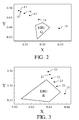
- Color point 14 corresponds to a green-emitting phosphor segment which contains 100% Zn 2 SiO 4 : Mn and color point 19 corresponds to a phosphor segment which contains 100% (Y 0.5 Gd 0.5 ) BO 3 : Tb.
- the color points 15 to 18 are the color points of green-emitting phosphor segments which contain a heterogeneous mixture of Zn 2 SiO 4 : Mn and (Y 0.5 Gd 0.5 ) BO 3 : Tb.
- the assignment of the color dots to the respective proportion of the phosphors in the green-emitting phosphor segment is shown in Table 4.
- EBU G is the EBU standard for green. Assignment of color points 15 to 18 Color point no.
- Color point 20 corresponds to a red-emitting phosphor segment which contains 100% (Y, Gd) BO 3 : Eu and color point 25 corresponds to a red-emitting phosphor segment which contains 100% Y (V, P) O 4 : Eu.
- the color points 21 to 24 are the color points of red-emitting phosphor segments which contain a heterogeneous mixture of (Y, Gd) BO 3 : Eu and Y (V, P) O 4 : Eu.
- the assignment of the color points to the respective proportion of the phosphors in the red-emitting phosphor segment is shown in Table 5.
- EBU R is the EBU standard for red. Assignment of color dots 21 to 24 Color point no.
- both dry coating processes e.g. B. electrostatic Deposition or electrostatically assisted dusting, as well as wet coating processes, z. B. screen printing, dispenser processes in which a suspension with one is introduced along the channels moving nozzle, or sedimentation from the liquid phase.
- the two phosphors of a color segment must be in Water, an organic solvent, optionally together with a dispersant, a surfactant and an anti-foaming agent or a binder preparation be dispersed.
- a dispersant for plasma screens inorganic binders that have an operating temperature of 250 ° C without decomposition, Resist embrittlement or discoloration, or organic binders that later show through Oxidation can be removed.
- the carrier plate 2 After the application of the phosphor layer 9 on a carrier plate 2, which address electrodes 10 and has a rib structure 12 with separating ribs, the carrier plate 2 with other components such as a front panel 1 and an inert gas mixture used to make a plasma screen.
- the noble gas mixture can Xenon with a proportion between 5 and 30% by volume, preferably 10% by volume contain.
- One or more color segments can be heterogeneous in a plasma display Mixture of at least two phosphors that emit the same color. It is particularly preferred that the red, green and blue emitting in a plasma screen Has color segments in the phosphor layer 9, each color segment one heterogeneous mixture of at least two phosphors that emit the same color, contains.
- a monochrome plasma screen can also be produced.
- the phosphor layer 9 contains only a heterogeneous mixture of at least two Phosphors that emit the same color.
- a screen printing paste was first prepared, containing 30% by weight (Y, Gd) BO 3 : Tb, 20% by weight Zn 2 SiO 4 : Mn and 50% of an organic binder.
- the paste was applied to a carrier plate 2 made of glass with a rib structure 12 and address electrodes made of Ag by means of screen printing and dried. This process step is carried out one after the other for the other two types of fluorescent with the emission colors red and blue.
- the screen printing paste for the red color segment contained 50% by weight (Y, Gd) BO 3 : Eu and 50% of an organic binder.
- the screen printing paste for the blue color segment contained 50% by weight of BaMgAl 10 O 17 : Eu and 50% of an organic binder.
- This carrier plate 2 was together with a front plate made of glass, which is a dielectric Layer 4 made of PbO-containing glass, a protective layer 5 made of MgO and discharge electrodes 6.7 from ITO, used to build an AC plasma screen.
- a front plate made of glass which is a dielectric Layer 4 made of PbO-containing glass, a protective layer 5 made of MgO and discharge electrodes 6.7 from ITO, used to build an AC plasma screen.
- a front plate made of glass which is a dielectric Layer 4 made of PbO-containing glass, a protective layer 5 made of MgO and discharge electrodes 6.7 from ITO, used to build an AC plasma screen.
- a front plate made of glass which is a dielectric Layer 4 made of PbO-containing glass, a protective layer 5 made of MgO and discharge electrodes 6.7 from ITO, used to build an AC plasma screen.
- a mixture of 10% by volume Xe and 90% by volume Ne was used for gas filling.
- the plasma screen showed greater efficiency and improved Peak luminance on.
- a screen printing paste was first prepared, containing 30% by weight: (Y, Gd) BO 3 : Eu, 20% by weight Y (V, P) O 4 : Eu and 50% of an organic binder.
- the paste was applied to a carrier plate 2 made of glass with a rib structure 12 and address electrodes made of Ag by means of screen printing and dried. This process step is carried out one after the other for the other two types of fluorescent material with the emission colors green and blue.
- the screen printing paste for the green color segment contained 50% by weight of Zn 2 SiO 4 : Mn and 50% of an organic binder.
- the screen printing paste for the blue color segment contained 50% by weight of BaMgAl 10 O 17 : Eu and 50% of an organic binder. All additives remaining in the phosphor layer 9 were removed by thermal treatment of the support plate 2 between 400 and 600 ° C. in an oxygen-containing atmosphere.
- This carrier plate 2 was together with other components as in the embodiment 1 described, used to build a plasma screen.
- a screen printing paste containing 30% by weight: BaMgAl 10 O 17 : Eu, 20% by weight YBO 3 : Ce and 50% of an organic binder was first prepared.
- the paste was applied to a carrier plate 2 made of glass with a rib structure 12 and address electrodes made of Ag by means of screen printing and dried. This process step is carried out one after the other for the other two types of fluorescent with the emission colors red and green.
- the screen printing paste for the green color segment contained 50% by weight of Zn 2 SiO 4 : Mn and 50% of an organic binder.
- the screen printing paste for the red color segment contained 50% by weight (Y, Gd) BO 3 : Eu and 50% of an organic binder.
- This carrier plate 2 was together with other components as in the embodiment 1 described, used to build a plasma screen.
- a screen printing paste was first prepared, containing 30% by weight (Y, Gd) BO 3 : Tb, 20% by weight Zn 2 SiO 4 : Mn and 50% of an organic binder.
- the paste was applied to a carrier plate 2 made of glass with a rib structure 12 and address electrodes made of Ag by means of screen printing and dried. This process step is carried out one after the other for the other two types of fluorescent with the emission colors red and blue.
- the screen printing paste for the red color segment contained 30% by weight: (Y, Gd) BO 3 : Eu, 20% by weight Y (V, P) O 4 : Eu and 50% of an organic binder.
- the screen printing paste for the blue color segment contained 30% by weight: BaMgAl 10 O 17 : Eu, 20% by weight YBO 3 : Ce and 50% of an organic binder.
- This carrier plate 2 was together with other components as in the embodiment 1, used to build an improved plasma display.
Landscapes
- Chemical & Material Sciences (AREA)
- Engineering & Computer Science (AREA)
- Inorganic Chemistry (AREA)
- Materials Engineering (AREA)
- Organic Chemistry (AREA)
- Physics & Mathematics (AREA)
- Plasma & Fusion (AREA)
- Luminescent Compositions (AREA)
- Gas-Filled Discharge Tubes (AREA)
Abstract
Description
Weiterhin ist es bevorzugt, dass ein Farbsegment der Leuchtstoffschicht eine heterogene Mischung aus Zn2SiO4:Mn und einem Tb3+-aktivierten Leuchtstoff enthält.
- Fig. 1
- den Aufbau und das Funktionsprinzip einer einzelnen Plasmazelle in einem AC-Plasmabildschirm.
| Abklingzeiten und Farbpunkte geeigneter blau-emittierender Ce3+- und Tm3+-aktivierter Leuchtstoffe | ||
| Leuchtstoff | Abklingzeit [ms] | Farbpunkt [x,y] |
| YBO3:Ce | <0.1 | 0.165, 0.027 |
| (Y0.5Gd0.5)BO3:Ce | <0.1 | 0.168, 0.030 |
| LaBO3:Tm | < 0.1 | 0.168, 0.060 |
| Abklingzeiten und Farbpunkte geeigneter Tb3+-aktivierter Leuchtstoffe | ||
| Leuchtstoff | Abklingzeit [ms] | Farbpunkt [x,y] |
| LaPO4:Ce,Tb | 7.5 | 0.352, 0.580 |
| Y2SiO5:Tb | 5.0 | 0.331, 0.584 |
| GdMgB5O10:Ce,Tb | 5.5 | 0.343, 0.585 |
| CeMgAl11O19:Tb | 7.0 | 0.329, 0.605 |
| GdBO3:Tb | 8.0 | 0.336, 0.612 |
| (Y0.5Gd0.5)BO3:Tb | 8.0 | 0.338, 0.615 |
| YBO3:Tb | 8.0 | 0.338, 0.615 |
| InBO3:Tb | 16.0 | 0.331, 0.621 |
| Abklingzeiten und Farbpunkte geeigneter rot-emittierender Eu2+-Leuchtstoffe | ||
| Leuchtstoff | Abklingzeit [ms] | Farbpunkt [x,y] |
| Y2O3:Eu | 2.5 | 0.642, 0.344 |
| YVO4:Eu | 3.5 | 0.658, 0.326 |
| Y(V,P)O4:Eu | 3.5 | 0.662, 0.328 |
| (Y0.5Gd0.5)2O3:Eu | 2.5 | 0.650, 0.337 |
| Zuordnung der Farbpunkte 15 bis 18 | |
| Farbpunkt Nr. | Anteil der Leuchtstoffe |
| 15 | 80 % Zn2SiO4:Mn, 20 % (Y0.5Gd0.5)BO3:Tb |
| 16 | 60 % Zn2SiO4:Mn, 40 % (Y0.5Gd0.5)BO3:Tb |
| 17 | 40 % Zn2SiO4:Mn, 80 % (Y0.5Gd0.5)BO3:Tb |
| 18 | 20 % Zn2SiO4:Mn, 20 % (Y0.5Gd0.5)BO3:Tb |
| Zuordnung der Farbpunkte 21 bis 24 | |
| Farbpunkt Nr. | Anteil der Leuchtstoffe |
| 21 | 80 % (Y,Gd)BO3:Eu, 20 % Y(V,P)O4:Eu |
| 22 | 60 % (Y,Gd)BO3:Eu, 40 % Y(V,P)O4:Eu |
| 23 | 40 % (Y,Gd)BO3:Eu, 80 % Y(V,P)O4:Eu |
| 24 | 20 % (Y,Gd)BO3:Eu, 20 % Y(V,P)O4:Eu |
Durch thermische Behandlung der Trägerplatte 2 zwischen 400 und 600 °C in sauerstoffhaltiger Atmosphäre wurden alle in der Leuchtstoffschicht 9 verbliebenen Additive entfernt.
Claims (9)
- Plasmabildschirm ausgerüstet mit einer Frontplatte (1), die eine Glasplatte (3), auf der eine dielektrische Schicht (4) und eine Schutzschicht (5) aufgebracht sind, aufweist, mit einer Trägerplatte (2) ausgestattet mit einer Leuchtstoffschicht (9), die eine heterogene Mischung aus mindestens zwei Leuchtstoffen enthält, die dieselbe Farbe emittieren, mit einer Rippenstruktur (12), die den Raum zwischen Frontplatte (1) und Trägerplatte (2) in Plasmazellen, die mit einem Gas gefüllt sind, aufteilt, und mit einem oder mehreren Elektroden-Arrays (6,7,10) auf der Frontplatte (1) und der Trägerplatte (2) zur Erzeugung von stillen elektrischen Entladungen in den Plasmazellen.
- Plasmabildschirm nach Anspruch 1,
dadurch gekennzeichnet, dass die Leuchtstoffschicht (9) in verschiedene Farbsegmente unterteilt ist und wenigstens ein Farbsegment eine heterogene Mischung aus mindestens zwei Leuchtstoffen, die dieselbe Farbe emittieren, enthält. - Plasmabildschirm nach Anspruch 2,
dadurch gekennzeichnet, dass ein Farbsegment der Leuchtstoffschicht (9) eine heterogene Mischung aus BaMgAl10O17:Eu und einem Leuchtstoff ausgewählt der aus der Gruppe der Ce3+-aktivierten Leuchtstoffe und der Tm3+-aktivierten Leuchtstoffe enthält. - Plasmabildschirm nach Anspruch 3,
dadurch gekennzeichnet, dass der Ce3+-aktivierte Leuchtstoff ausgewählt ist aus der Gruppe YBO3:Ce und (Y1-xGdx)BO3:Ce mit 0 ≤ x ≤ 1. - Plasmabildschirm nach Anspruch 3,
dadurch gekennzeichnet, dass der Tm3+-aktivierte Leuchtstoff LaBO3:Tm ist. - Plasmabildschirm nach Anspruch 2,
dadurch gekennzeichnet, dass ein Farbsegment der Leuchtstoffschicht (9) eine heterogene Mischung aus Zn2SiO4:Mn und einem Tb3+-aktivierten Leuchtstoff enthält. - Plasmabildschirm nach Anspruch 6,
dadurch gekennzeichnet, dass der Tb3+-aktivierte Leuchtstoff ausgewählt ist aus der Gruppe LaPO4:Ce,Tb,Y2SiO5:Tb, GdMgB5O10:Ce,Tb, CeMgAl11O19:Tb, GdBO3:Tb, (Y1-xGdx)BO3:Tb mit 0 ≤ x ≤ 1, YBO3:Tb und InBO3:Tb. - Plasmabildschirm nach Anspruch 2,
dadurch gekennzeichnet, dass ein Farbsegment der Leuchtstoffschicht (9) eine heterogene Mischung aus (Y,Gd)BO3:Eu und einem zweiten, rot-emittierenden Leuchtstoff, dessen Farbpunkt (x,y) einen y-Wert < 0.36 aufweist, enthält. - Plasmabildschirm nach Anspruch 8,
dadurch gekennzeichnet, dass der zweite, rot-emittierende Leuchtstoff ausgewählt ist aus der Gruppe Y2O3:Eu, YVO4:Eu, Y(V,P)O4:Eu und (Y1-xGdx)2O3:Eu mit 0 ≤ x ≤ 1.
Applications Claiming Priority (2)
| Application Number | Priority Date | Filing Date | Title |
|---|---|---|---|
| DE10061720 | 2000-12-12 | ||
| DE10061720A DE10061720A1 (de) | 2000-12-12 | 2000-12-12 | Plasmabildschirm mit Leuchtstoffschicht |
Publications (3)
| Publication Number | Publication Date |
|---|---|
| EP1215698A2 true EP1215698A2 (de) | 2002-06-19 |
| EP1215698A3 EP1215698A3 (de) | 2005-02-09 |
| EP1215698B1 EP1215698B1 (de) | 2007-08-08 |
Family
ID=7666731
Family Applications (1)
| Application Number | Title | Priority Date | Filing Date |
|---|---|---|---|
| EP01000719A Expired - Lifetime EP1215698B1 (de) | 2000-12-12 | 2001-12-06 | Plasmabildschirm mit Leuchtstoffschicht |
Country Status (7)
| Country | Link |
|---|---|
| US (1) | US6794821B2 (de) |
| EP (1) | EP1215698B1 (de) |
| JP (2) | JP4197098B2 (de) |
| KR (1) | KR100898199B1 (de) |
| CN (1) | CN100557752C (de) |
| DE (2) | DE10061720A1 (de) |
| TW (1) | TW528997B (de) |
Cited By (2)
| Publication number | Priority date | Publication date | Assignee | Title |
|---|---|---|---|---|
| EP1890311A4 (de) * | 2006-02-23 | 2008-08-20 | Matsushita Electric Industrial Co Ltd | Plasmaanzeigegerät und verfahren zur herstellung eines materials aus grünem phosphor für das plasmaanzeigegerät |
| EP2331345B2 (de) † | 2008-10-09 | 2018-02-21 | Bundesdruckerei GmbH | Sicherheitsmerkmal auf basis lumineszenz emittierender stoffe |
Families Citing this family (16)
| Publication number | Priority date | Publication date | Assignee | Title |
|---|---|---|---|---|
| TWI224806B (en) * | 2000-05-12 | 2004-12-01 | Semiconductor Energy Lab | Semiconductor device and manufacturing method thereof |
| TWI290329B (en) * | 2001-10-30 | 2007-11-21 | Hitachi Ltd | Plasma display device, luminescent device and image and information display system using the same |
| KR100490540B1 (ko) * | 2002-11-06 | 2005-05-17 | 삼성에스디아이 주식회사 | 플라즈마 디스플레이 패널 |
| KR100533723B1 (ko) * | 2003-04-25 | 2005-12-06 | 엘지전자 주식회사 | 플라즈마 디스플레이 패널 및 그 제조방법 |
| KR100651277B1 (ko) | 2003-07-25 | 2006-11-28 | 엘지전자 주식회사 | 녹색형광체 및 플라즈마 디스플레이 패널 |
| JP2005116363A (ja) * | 2003-10-08 | 2005-04-28 | Pioneer Plasma Display Corp | プラズマディスプレイパネル |
| KR100669408B1 (ko) * | 2003-11-24 | 2007-01-15 | 삼성에스디아이 주식회사 | 플라즈마 디스플레이 패널 |
| KR100627355B1 (ko) * | 2003-11-28 | 2006-09-21 | 삼성에스디아이 주식회사 | 플라즈마 디스플레이 패널 |
| JP4541832B2 (ja) * | 2004-03-19 | 2010-09-08 | パナソニック株式会社 | プラズマディスプレイパネル |
| KR100918417B1 (ko) * | 2004-05-28 | 2009-09-24 | 삼성에스디아이 주식회사 | 플라즈마 디스플레이 패널 |
| KR20060082527A (ko) * | 2005-01-12 | 2006-07-19 | 삼성에스디아이 주식회사 | 형광체 및 이를 이용한 플라즈마 디스플레이 패널 |
| US7662317B2 (en) * | 2005-06-30 | 2010-02-16 | Samsung Electronics Co., Ltd. | Dispersant, paste composition including the dispersant, inorganic device using the paste composition, and display apparatus including the inorganic device |
| KR101178053B1 (ko) * | 2005-09-27 | 2012-08-30 | 삼성전자주식회사 | 카르복실 에스테르계 분산제 및 그를 포함하는 황화물계 형광체 페이스트 조성물 |
| KR100904809B1 (ko) * | 2006-02-23 | 2009-06-25 | 파나소닉 주식회사 | 플라즈마디스플레이장치용 녹색형광체 재료의 제조방법 |
| WO2010016140A1 (ja) * | 2008-08-08 | 2010-02-11 | 株式会社 日立製作所 | 平面表示パネルの制御方法及びプラズマディスプレイパネルの制御方法 |
| JP2010097861A (ja) * | 2008-10-17 | 2010-04-30 | Hitachi Ltd | 表示装置およびプラズマディスプレイパネル |
Family Cites Families (15)
| Publication number | Priority date | Publication date | Assignee | Title |
|---|---|---|---|---|
| KR0133524B1 (ko) * | 1988-12-28 | 1998-04-20 | 아라이 기꾸지 | 형광체 |
| JPH04161483A (ja) * | 1990-10-25 | 1992-06-04 | Kasei Optonix Co Ltd | 発光組成物及び陰極線管用蛍光面 |
| MY109224A (en) * | 1993-02-11 | 1996-12-31 | Samsung Display Devices Co Ltd | Mixed blue emitting phosphor. |
| JPH09219154A (ja) * | 1996-02-08 | 1997-08-19 | Japan Synthetic Rubber Co Ltd | 螢光体組成物およびプラズマディスプレイパネル |
| KR100232136B1 (ko) * | 1996-08-20 | 1999-12-01 | 구자홍 | 칼라 플라즈마 디스플레이 패널의 격벽구조 및 격벽제조방법 |
| JPH10149776A (ja) * | 1996-11-18 | 1998-06-02 | Kasei Optonix Co Ltd | プラズマディスプレイ用蛍光膜 |
| US6013309A (en) * | 1997-02-13 | 2000-01-11 | Lg Electronics Inc. | Protection layer of plasma display panel and method of forming the same |
| JPH10255671A (ja) * | 1997-03-11 | 1998-09-25 | Toray Ind Inc | 蛍光体ペースト |
| DE19727607C2 (de) | 1997-06-28 | 2000-11-23 | Philips Corp Intellectual Pty | Plasmabildschirm mit einer UV-Leuchtstoffzubereitung und UV-Leuchtstoffzubereitung |
| JP4151104B2 (ja) * | 1998-03-31 | 2008-09-17 | 株式会社日立製作所 | プラズマディスプレイ |
| WO2000024025A1 (en) * | 1998-10-20 | 2000-04-27 | Koninklijke Philips Electronics N.V. | Plasma display panel |
| JP2000251701A (ja) * | 1999-02-26 | 2000-09-14 | Toray Ind Inc | ディスプレイの製造方法 |
| US6210605B1 (en) * | 1999-07-26 | 2001-04-03 | General Electric Company | Mn2+ activated green emitting SrAL12O19 luminiscent material |
| JP3797084B2 (ja) * | 1999-12-14 | 2006-07-12 | 松下電器産業株式会社 | プラズマディスプレイ装置 |
| DE10043530A1 (de) * | 2000-09-05 | 2002-03-14 | Philips Corp Intellectual Pty | Farbbildschirm mit blauer Leuchtstoffschicht |
-
2000
- 2000-12-12 DE DE10061720A patent/DE10061720A1/de not_active Withdrawn
-
2001
- 2001-12-06 US US10/011,893 patent/US6794821B2/en not_active Expired - Fee Related
- 2001-12-06 EP EP01000719A patent/EP1215698B1/de not_active Expired - Lifetime
- 2001-12-06 DE DE50112824T patent/DE50112824D1/de not_active Expired - Lifetime
- 2001-12-07 TW TW090130384A patent/TW528997B/zh not_active IP Right Cessation
- 2001-12-07 CN CNB011454911A patent/CN100557752C/zh not_active Expired - Fee Related
- 2001-12-10 KR KR1020010077904A patent/KR100898199B1/ko not_active Expired - Fee Related
- 2001-12-12 JP JP2001378214A patent/JP4197098B2/ja not_active Expired - Fee Related
-
2008
- 2008-04-03 JP JP2008096998A patent/JP4904307B2/ja not_active Expired - Fee Related
Cited By (3)
| Publication number | Priority date | Publication date | Assignee | Title |
|---|---|---|---|---|
| EP1890311A4 (de) * | 2006-02-23 | 2008-08-20 | Matsushita Electric Industrial Co Ltd | Plasmaanzeigegerät und verfahren zur herstellung eines materials aus grünem phosphor für das plasmaanzeigegerät |
| US7705537B2 (en) | 2006-02-23 | 2010-04-27 | Panasonic Corporation | Plasma display device |
| EP2331345B2 (de) † | 2008-10-09 | 2018-02-21 | Bundesdruckerei GmbH | Sicherheitsmerkmal auf basis lumineszenz emittierender stoffe |
Also Published As
| Publication number | Publication date |
|---|---|
| US6794821B2 (en) | 2004-09-21 |
| EP1215698B1 (de) | 2007-08-08 |
| JP2002251962A (ja) | 2002-09-06 |
| JP2008177174A (ja) | 2008-07-31 |
| JP4197098B2 (ja) | 2008-12-17 |
| TW528997B (en) | 2003-04-21 |
| KR100898199B1 (ko) | 2009-05-18 |
| DE10061720A1 (de) | 2002-06-13 |
| CN1360328A (zh) | 2002-07-24 |
| US20020113552A1 (en) | 2002-08-22 |
| DE50112824D1 (de) | 2007-09-20 |
| CN100557752C (zh) | 2009-11-04 |
| JP4904307B2 (ja) | 2012-03-28 |
| EP1215698A3 (de) | 2005-02-09 |
| KR20020046212A (ko) | 2002-06-20 |
Similar Documents
| Publication | Publication Date | Title |
|---|---|---|
| DE69824053T2 (de) | Lumineszenzmittel, pulverförmiges Lumineszenzmittel, Plasma-Anzeigetafel, und Herstellungsverfahren derselben | |
| EP1215698B1 (de) | Plasmabildschirm mit Leuchtstoffschicht | |
| DE19534075C2 (de) | Phosphor | |
| EP1156507B1 (de) | Plasmabildschirm mit einem Terbium(III)-aktivierten Leuchtstoff | |
| DE10009915A1 (de) | Plasmabildschirm mit UV-Licht emittierender Schicht | |
| DE60300743T2 (de) | Grüner Leuchtstoff und seine Verwendung in Vorrichtungen | |
| DE19937420C1 (de) | Plasmabildschirm mit Leuchtstoffzubereitung, Leuchtstoffzubereitung und Verfahren zu Herstellung einer Leuchtstoffzubereitung | |
| EP1256616B1 (de) | Plasmabildschirm mit blauem Leuchtstoff | |
| EP1158559A2 (de) | Plasmabildschirm mit Terbium(III)-aktiviertem Leuchtstoff | |
| EP1130621A2 (de) | Plasmabildschirm mit blauem Leuchtstoff | |
| EP1118650A2 (de) | Plasmabildschirm mit rotem Leuchtstoff | |
| EP1187167B1 (de) | Farbbildschirm mit blauer Leuchtstoffschicht | |
| DE19851348A1 (de) | Lumineszierender Schirm mit oxidhaltiger Leuchtstoffzubereitung | |
| WO2004021397A1 (de) | Dielektrische barriere-entladungslampe mit verbesserter farbwiedergabe | |
| DE60313312T2 (de) | Plasmaanzeigetafel enthaltend eine terbium(iii)-aktivierte fluoreszierende substanz | |
| EP1103591A1 (de) | Plasmabildschirm mit rotem Leuchtstoff | |
| EP1296348A2 (de) | Plasmabildschirm mit erhöhter Effizienz | |
| DE60204724T2 (de) | Plasmabildschirm mit grünem phosphor | |
| DE102004054091A1 (de) | Durch Vakuum-ultraviolett angeregtes grünes Phosphormaterial und eine dieses Material verwendende Vorrichtung | |
| EP1258902A2 (de) | Plasmabildschirm mit verbessertem Weissfarbpunkt | |
| DE10254175A1 (de) | Plasmabildschirm mit blauemittierendem Leuchtstoff | |
| EP1229099A2 (de) | Plasmabildschirm mit einer Leuchtstoffschicht | |
| DE10210043A1 (de) | Plasmabildschirm mit Pr(III)-aktiviertem Leuchtstoff | |
| DE3004535C2 (de) | Fluoreszierendes Material mit einem Gehalt an Indiumoxid | |
| DE10215891A1 (de) | Plasmabildschirm mit erhöhter Effizienz |
Legal Events
| Date | Code | Title | Description |
|---|---|---|---|
| PUAI | Public reference made under article 153(3) epc to a published international application that has entered the european phase |
Free format text: ORIGINAL CODE: 0009012 |
|
| AK | Designated contracting states |
Kind code of ref document: A2 Designated state(s): AT BE CH CY DE DK ES FI FR GB GR IE IT LI LU MC NL PT SE TR |
|
| AX | Request for extension of the european patent |
Free format text: AL;LT;LV;MK;RO;SI |
|
| RAP1 | Party data changed (applicant data changed or rights of an application transferred) |
Owner name: PHILIPS CORPORATE INTELLECTUAL PROPERTY GMBH Owner name: KONINKLIJKE PHILIPS ELECTRONICS N.V. |
|
| RAP1 | Party data changed (applicant data changed or rights of an application transferred) |
Owner name: PHILIPS INTELLECTUAL PROPERTY & STANDARDS GMBH Owner name: KONINKLIJKE PHILIPS ELECTRONICS N.V. |
|
| PUAL | Search report despatched |
Free format text: ORIGINAL CODE: 0009013 |
|
| AK | Designated contracting states |
Kind code of ref document: A3 Designated state(s): AT BE CH CY DE DK ES FI FR GB GR IE IT LI LU MC NL PT SE TR |
|
| AX | Request for extension of the european patent |
Extension state: AL LT LV MK RO SI |
|
| RIC1 | Information provided on ipc code assigned before grant |
Ipc: 7H 01J 17/49 B Ipc: 7C 09K 11/20 B Ipc: 7H 01J 17/16 B Ipc: 7H 01J 1/63 A |
|
| 17P | Request for examination filed |
Effective date: 20050809 |
|
| AKX | Designation fees paid |
Designated state(s): DE FR GB |
|
| GRAP | Despatch of communication of intention to grant a patent |
Free format text: ORIGINAL CODE: EPIDOSNIGR1 |
|
| RIC1 | Information provided on ipc code assigned before grant |
Ipc: H01J 17/49 20060101ALI20070130BHEP Ipc: H01J 17/16 20060101AFI20070130BHEP |
|
| GRAS | Grant fee paid |
Free format text: ORIGINAL CODE: EPIDOSNIGR3 |
|
| GRAA | (expected) grant |
Free format text: ORIGINAL CODE: 0009210 |
|
| AK | Designated contracting states |
Kind code of ref document: B1 Designated state(s): DE FR GB |
|
| REG | Reference to a national code |
Ref country code: GB Ref legal event code: FG4D Free format text: NOT ENGLISH |
|
| REF | Corresponds to: |
Ref document number: 50112824 Country of ref document: DE Date of ref document: 20070920 Kind code of ref document: P |
|
| GBT | Gb: translation of ep patent filed (gb section 77(6)(a)/1977) |
Effective date: 20070912 |
|
| ET | Fr: translation filed | ||
| PLBE | No opposition filed within time limit |
Free format text: ORIGINAL CODE: 0009261 |
|
| STAA | Information on the status of an ep patent application or granted ep patent |
Free format text: STATUS: NO OPPOSITION FILED WITHIN TIME LIMIT |
|
| 26N | No opposition filed |
Effective date: 20080509 |
|
| REG | Reference to a national code |
Ref country code: GB Ref legal event code: 732E Free format text: REGISTERED BETWEEN 20100204 AND 20100211 |
|
| REG | Reference to a national code |
Ref country code: FR Ref legal event code: TP |
|
| REG | Reference to a national code |
Ref country code: FR Ref legal event code: RM |
|
| PGFP | Annual fee paid to national office [announced via postgrant information from national office to epo] |
Ref country code: GB Payment date: 20131112 Year of fee payment: 13 Ref country code: FR Payment date: 20131115 Year of fee payment: 13 Ref country code: DE Payment date: 20131113 Year of fee payment: 13 |
|
| REG | Reference to a national code |
Ref country code: DE Ref legal event code: R119 Ref document number: 50112824 Country of ref document: DE |
|
| GBPC | Gb: european patent ceased through non-payment of renewal fee |
Effective date: 20141206 |
|
| REG | Reference to a national code |
Ref country code: FR Ref legal event code: ST Effective date: 20150831 |
|
| PG25 | Lapsed in a contracting state [announced via postgrant information from national office to epo] |
Ref country code: DE Free format text: LAPSE BECAUSE OF NON-PAYMENT OF DUE FEES Effective date: 20150701 Ref country code: GB Free format text: LAPSE BECAUSE OF NON-PAYMENT OF DUE FEES Effective date: 20141206 |
|
| PG25 | Lapsed in a contracting state [announced via postgrant information from national office to epo] |
Ref country code: FR Free format text: LAPSE BECAUSE OF NON-PAYMENT OF DUE FEES Effective date: 20141231 |