EP1215734A2 - Dispositif semi-conducteur de protection contre les surtensions et procédé pour sa fabrication - Google Patents
Dispositif semi-conducteur de protection contre les surtensions et procédé pour sa fabrication Download PDFInfo
- Publication number
- EP1215734A2 EP1215734A2 EP01129517A EP01129517A EP1215734A2 EP 1215734 A2 EP1215734 A2 EP 1215734A2 EP 01129517 A EP01129517 A EP 01129517A EP 01129517 A EP01129517 A EP 01129517A EP 1215734 A2 EP1215734 A2 EP 1215734A2
- Authority
- EP
- European Patent Office
- Prior art keywords
- layers
- buried
- conductivity type
- semiconductor substrate
- semiconductor device
- Prior art date
- Legal status (The legal status is an assumption and is not a legal conclusion. Google has not performed a legal analysis and makes no representation as to the accuracy of the status listed.)
- Withdrawn
Links
Images


Classifications
-
- H—ELECTRICITY
- H10—SEMICONDUCTOR DEVICES; ELECTRIC SOLID-STATE DEVICES NOT OTHERWISE PROVIDED FOR
- H10D—INORGANIC ELECTRIC SEMICONDUCTOR DEVICES
- H10D8/00—Diodes
- H10D8/01—Manufacture or treatment
- H10D8/041—Manufacture or treatment of multilayer diodes
-
- H—ELECTRICITY
- H10—SEMICONDUCTOR DEVICES; ELECTRIC SOLID-STATE DEVICES NOT OTHERWISE PROVIDED FOR
- H10D—INORGANIC ELECTRIC SEMICONDUCTOR DEVICES
- H10D8/00—Diodes
- H10D8/80—PNPN diodes, e.g. Shockley diodes or break-over diodes
Definitions
- the present invention relates to the technical field of semiconductor devices, and in particular to the structure of surge protective component.
- two terminal surge protective components are widely used as semiconductor devices for protecting electronic circuits from surge voltages occurring due to lightening strikes, etc.
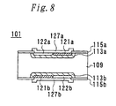
- Numeral 101 in FIG. 8 is an example of a semiconductor device of the related art.
- P-type base layers 113a and 113b are provided at a portion in the vicinity of both the inner side surface and the reverse side surface of an N-type substrate 109 so that a PN junction is formed between the substrate 109 and the base layers 113a and 113b.
- the base layers 113a and 113b are positioned substantially in the vicinity of the center of the semiconductor device 101, and are patterned so as to be rectangular in shape, with rounded corners.
- N-type emitters 122a and 122b are arranged at a part in the vicinity of the surface of the inside of the base layers 113a and 113b so that a PN junction is formed between each of the emitter layers 122a and 122b and the base layers 113a and 113b.
- Ohmic layers 121a and 121b with a high P-type surface concentration are provided at a portion where the emitter layers 122a and 122b provided in the vicinity of the surface on the inside of the base layers 113a and 113b are not provided.
- Metal films 127a and 127b are formed at the surfaces of the emitter layers 122a and 122b and the ohmic layers 121a and 121b on the surface side and rear surface side of the substrate 109.
- the metal film 127a at the surface side is electrically connected to the surface side emitter layer 122a and the ohmic layer 121a, but is not connected to the substrate 109.
- the metal film 127b of the rear surface side is electrically connected to the surface side emitter layer 122b and the ohmic layer 121b, but is not connected to the substrate 109.
- the semiconductor device 101 of this structure has a four-layer PNPN structure when viewed from the surface side or from the rear side. This means that the PN junction between the base layers 113a and 113b and the substrate 109 is reverse biased for whichever of the metal films 127a and 127b a voltage is applied to, wherein a current flows as a result of this PN junction experiencing an avalanche breakdown.
- the PNPN structure latches up, and a voltage state lower than a voltage during avalanche breakdown is maintained between the metal films 127a and 127b. Therefore, when the semiconductor device 101 is connected in parallel with an electronic circuit, when a surge voltage is applied to the electronic circuit, the semiconductor device 101 conducts in such a manner that the surge voltage is not applied to the electronic circuit.
- the present invention sets out to resolve the problems encountered in the related art, it is the object of the present invention to provide a surge protection semiconductor device that has a straightforward manufacturing process, a simple structure, and is highly reliable.
- a semiconductor device of the present invention having, when one of either an N-type or P-type is defined as a first conductivity type, and the other is defined as a second conductivity type, a semiconductor substrate of the first conductivity type, comprises first and second buried layers (in this invention, a buried layer may include a layer being partially exposed on the surface of a semiconductor substrate 9 as shown in Fig. 6) provided within the semiconductor substrate, being of the first conductivity type, and being of a higher concentration than the semiconductor substrate, first and second emitter layers of the first conductivity type, first and second base layers of the second conductivity type, and a substrate layer constituted by the semiconductor substrate. The substrate layer is sandwiched between the first and second buried layers.
- At least a part of the first and second base layers are positioned on one side surface and the other side surface of the semiconductor substrate so as to form PN junctions with the first and second buried layers. At least a part of the first and second emitter layers are located in a vicinity of a surface inside of the first and second base layers so as to form PN junctions with the first and second base layers.
- the first and second base layers are respectively provided between the first and second emitter layers and the first and second buried layers, and the first and second buried layers are located between the first and second base layers and the substrate layer.
- the first and second metal films are formed on both sides of the semiconductor substrate, the first emitter layer and the first base layer are electrically short-circuited by the first metal film; and the second emitter layer and the second base layer are electrically short-circuited by the second metal film.
- first and second moats with bottom surfaces reaching the buried layers are formed on both sides of the semiconductor substrate and the first and second emitter layers are located on inside of the first and second moats.
- the insides of the first and second moats of this semiconductor device of the present invention are filled with oxide.
- first and second base layers are positioned at a region on outside of the first and second moats of surfaces of the semiconductor substrate.
- At least a part of the first and second buried layers are positioned at a region on the outside of the first and second moats of the surfaces of the semiconductor substrate of the semiconductor device of the present invention.
- a semiconductor device manufacturing method of the present invention comprises the steps of, when one of an N-type and P-type is defined as a first conductivity type and the other is defined as a second conductivity type:
- the first and second buried layers are formed by introducing an impurity of the first conductivity type into the semiconductor substrate with the surfaces of both sides of the semiconductor substrate completely exposed and diffusing impurity of the first conductivity type.
- the first and second base layers are formed by introducing an impurity of the second conductivity type into the first and second buried layers with the surfaces of the first and second buried layers completely exposed and diffusing impurity of the second conductivity type.
- the semiconductor device manufacturing method of the present invention further comprises a step of, with ring-shaped moats having bottom surfaces reaching positions deeper than the bottom surfaces of the base layers, forming moats including the first and second emitter layers inside of the ring-shaped moats on both sides of the semiconductor substrate.
- the semiconductor device manufacturing method of the present invention may comprise a further step of forming first and second metal films short-circuiting the first and second emitter layers positioned inside of the ring-shaped moats and the first and second base layers after filling the insides of the first and second moats with oxide and forming first and second passivation films.
- the semiconductor device of the present invention is a two terminal semiconductor device used for protecting electronic circuits from surge voltages.
- the semiconductor device includes, when one of either an N-type or P-type is defined as a first conductivity type and the other is defined as a second conductivity type, a semiconductor substrate of the first conductivity type, first and second buried layers provided within the semiconductor substrate, being of the first conductivity type, and being of a higher concentration than the semiconductor substrate, first and second emitter layers of the first conductivity type, first and second base layers of the second conductivity type, and a substrate layer constituted by the semiconductor substrate.
- the semiconductor layer is sandwiched between the first and second buried layers; and the first and second base layers are positioned on one side surface and the other side surface of the semiconductor substrate so as to form PN junctions with the first and second buried layers.
- the first and second emitter layers are located in the vicinity of the surface of the inside of the first and second base layers so as to form PN junctions with the first and second base layers; and the first and second base layers are respectively provided between the first and second emitter layers and the first and second buried layers, while the first and second buried layers are located between the first and second base layers and the substrate layer.
- the first and second buried layers are formed by means of introducing impurities to within the semiconductor substrate with the surface side and rear surface side of the semiconductor being completely exposed. Processing to pattern the first and second buried layers is therefore unnecessary.
- the first and second base layers are arranged so as to be positioned in the vicinity of the inside surfaces of the first and second buried layers so that the first and second base layers form PN junctions between the first and second buried layers and a PN junction is not formed between the first and second base layers and the substrate layer.
- the first and second base layers are formed in such a manner that the entire surfaces of the first and second buried layers are exposed.
- first and second base layers are formed partially within the first and second buried layers, spherical junction portions and circular junction portions of a PN junction formed between the first and second base layers and the first and second buried layers are eliminated by the first and second moats so that only planar junction portions remain.
- the ends of a PN junction formed between the first and second base layers and the first and second buried layers are exposed within the first and second moats, but are not exposed at the surface of the semiconductor substrate.
- the inside of the first and second moats is filled up with oxide etc. and baked so as to form first and second passivation films without causing the electrical characteristics of the PN junction to deteriorate.
- the oxide may include glass granules comprising lead oxide, aluminum oxide, silicon oxide etc.
- a surge protective component of a preferred embodiment of a semiconductor device of the present invention and a method of manufacturing this surge protective component will now be described using the drawings.
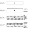
- FIG. 1(a) to FIG. 1(k) are views showing processes illustrating the method of manufacturing a semiconductor device of a first example of the present invention.
- the first conductivity type is an N-type (including N - , N + and N ++ types) and the second conductivity type is a P-type (including P - , P + and P ++ -types).
- a semiconductor substrate 9 consisting of high-resistivity N-type silicon single crystal is prepared.
- a crystal with a resistivity of 20 ⁇ cm or more, and less than or equal to 60 ⁇ cm (less than or equal to 2 ⁇ 10 14 cm 3 and greater than or equal to 7 ⁇ 10 13 cm 3 in concentration conversions) was used as the semiconductor substrate 9.
- phosphorous is implanted in with the entire surfaces of both sides of the semiconductor substrate 9 exposed; and as shown in FIG. 1(b), high concentration N-type layers 11a and 11b are formed in the vicinity of the surfaces of both of the inner surfaces of the semiconductor substrate 9.
- impurities contained in the high-concentration N-type layers 11a and 11b are diffused through heat processing so that first and second buried layers 12a and 12b of higher surface concentrations than the concentration of the semiconductor substrate 9 are formed.
- the surface of the first and second buried layers 12a and 12b coincide with the surface of the semiconductor substrate 9; and the depth of diffusion is substantially equal along the whole of the region for the first and second buried layers 12a and 12b.
- Numeral 10 in FIG. 1(c) indicates a substrate layer 10 constituting a low N-type concentration portion, such portion being a portion of the semiconductor substrate 9, except the first and second buried layers 12a and 12b.
- the first and second buried layers 12a and 12b are formed over both surfaces of the semiconductor substrate 9 in their entireties; and therefore sandwich the substrate layer 10.
- Numerals 19a and 19b show silicon oxide films formed on the surfaces of the buried layers 12a and 12b during a diffusion process.
- the silicon oxide films 19a and 19b are removed and boron is implated into the vicinity of the surfaces of the inner parts of the first and second buried layers 12a and 12b on the front and rear surfaces with the surfaces of the first and second buried layers 12a and 12b in an exposed state, as shown in FIG. 1(d).
- High-concentration P-type layers 14a and 14b are formed over the entire surfaces of the first and second buried layers 12a and 12b. In this state, the first and second buried layers 12a and 12b are buried in lower layers of the high-concentration P-type layers 14a and 14b.
- P-type first and second base layers 13a and 13b are formed in the vicinity of the inner part of both surfaces of the semiconductor substrate 9, as shown in Fig. 1(f).
- the positions of the bottom parts of the first and second base layers 13a and 13b exceed the bottom parts of the first and second buried layers 12a and 12b without being deep; and the first and second base layers 13a and 13b connect with the upper parts of the first and second buried layers 12a and 12b at this bottom part.
- the first and second base layers 13a and 13b therefore do not connect with the substrate layer 10.
- the first and second buried layers 12a and 12b are positioned on either side of the substrate layer 10; and the first and second base layers 13a and 13b are positioned at the side surfaces of the first and second buried layers 12a and 12b.
- PN junctions are formed between the first and second base layers 13a and 13b and the first and second buried layers 12a and 12b.
- Numerals 19a and 19b in FIG. 1(e) show silicon oxide films formed on the surfaces of the base layers 13a and 13b during the diffusion process, and silicon oxide films 19a and 19b are positioned on both sides of the semiconductor substrate 9.
- An opening of a large surface area is made at prescribed positions on the silicon oxide films 19a and 19b on the surfaces on both sides of the semiconductor substrate 9 using photographic processes and etching processes. After exposing the surfaces of the base layers 13a and 13b, boron is implanted into this exposed portion and a high-concentration P-type layer is formed.
- the numerals 15a and 15b in FIG. 1(f) indicate openings of a large surface area formed at the silicon oxide films 19a and 19b.
- Numerals 16a and 16b indicate high P-type concentration layers formed at the bottom surfaces of the openings 15a and 15b.
- mesh-like openings are made in the planar pattern at positions where the high P-type concentration layers 16a and 16b of the silicon oxide films 19a and 19b on both sides are not formed.
- the surfaces of the base layers 13a and 13b are then exposed, phosphorous is introduced, and a high N-type concentration layer is formed.
- Numerals 17a and 17b in FIG. 1(g) indicate mesh-like openings formed respectively at the silicon oxide films 19a and 19b on both sides and numerals 18a and 18b indicate high-concentration N-type layers formed at the bottom surfaces of the openings 17a and 17b.
- the planar shape of the high N-type concentration layers 18a and 18b is mesh-like.
- high-concentration P-type layers 16a and 16b and high-concentration N-type layers 18a and 18b are both formed in the vicinity of the inner surfaces of the base layers 13a and 13b.
- FIG. 1(h) shows the situation after diffusion where the silicon oxide films formed during diffusion processing are removed.
- first and second ohmic layers 21a and 21b are formed by diffusion of the high P-type concentration layers 16a and 16b; and first and second emitter layers 22a and 22b are formed by diffusion of the high-concentration N-type layers 18a and 18b.
- the depth of diffusion of the first and second ohmic layers 21a and 21b and the first and second emitter layers 22a and 22b is shallower than that of the first and second base layers 13a and 13b so that the first and second ohmic layers 21a and 21b and the outer portion of the surface shape of the first and second emitter layers 22a and 22b are located further towards the inside than the outer portion of the surface shape of the first and second base layers 13a and 13b.
- the first and second ohmic layers 21a and 21b and the first and second emitter layers 22a and 22b are formed on the insides of the first and second base layers 13a and 13b, respectively.
- a PN junction is therefore formed between the first and second emitter layers 22a and 22b and the first and second base layers 13a and 13b because these layers are of opposite conductivity types.
- first and second ohmic layers 21a and 21b and the first and second emitter layers 22a and 22b do not make contact with the first and second buried layers 12a and 12b or with the substrate layer 10.
- the pattern on one side of the semiconductor substrate 9 and on the other side is substantially the same in this state.
- This planar shape is shown in FIG. 4(a).
- the first and second emitter layers 22a and 22b are formed in the shape of a mesh. This means that the surfaces of the first and second base layers 13a and 13b are exposed in dotted state within the region where the surfaces of the first and second emitter layers 22a and 22b are positioned.
- FIG. 1(h) is a cross-section of a portion that does not include the first and second base layers 13a and 13b in a dotted state, corresponding to a cross-section taken along line A-A of FIG. 4(a).
- FIG. 2 is a cross-section of a portion that includes the surfaces of the first and second base layers 13a and 13b in a dotted state that corresponding to a cross-section taken along line B-B of FIG. 4(b).
- resist films having ring-shaped openings are formed on the front and rear surfaces of the semiconductor substrate 9, the semiconductor substrate 9, with the bottom surfaces of the openings exposed, is etched, and moats are formed.
- numeral 25a shows a first moat formed at one side surface of the semiconductor substrate 9 and numeral 25b shows a second moat formed in the surface on the other side.
- the ring-shaped openings of the resist films are located along a boundary of the first and second emitter layers 22a and 22b and the first and second base layers 13a and 13b, and the boundary of the first and second ohmic layers 21a and 21b and the first and second base layers 13a and 13b.
- the ring-shaped openings of the resist films are positioned above the edge portions of a region constituted by the first and second ohmic layers 21a and 21b and the first and second emitter layers 22a and 22b.
- the first and second moats 25a and 25b are formed in the same ring shape as the pattern for the openings for the resist films and are positioned above the edge portions of regions constituted by the first and second ohmic layers 21a and 21b and the first and second emitter layers 22a and 22b. That is, the first and second emitter layers 22a and 22b and the first and second ohmic layers 21a and 21b are positioned to the inside of the rings of the first and second moats 25a and 25b.
- the first and second moats 25a and 25b are deeper than the depth of the PN junction formed by the first and second base layers 13a and 13b and the first and second buried layers 12a and 12b; and therefore, the first and second moats 25a and 25b are only dug to depths that do not reach the substrate layer 10.
- the bottom parts of the first and second moats 25a and 25b are positioned in the first and second buried layers 12a and 12b. Therefore, an inner region and outer region of the first and second moats 25a and 25b of the first and second base layers 13a and 13b are electrically separated by the PN junction formed between the first and second base layers 13a and 13b and the first and second buried layers 12a and 12b.
- the PN junction formed between the first and second base layers 13a and 13b on the inside of the first and second moats 25a and 25b and the first and second buried layers 12a and 12b is therefore a planar junction.
- oxide is affixed to both sides of the semiconductor substrate 9 and an inside portion of a ring for the first and second moats 25a and 25b (and a scribe line portion for the semiconductor substrate 9 (not shown)) are exposed using photographic and etching processes after baking.
- first and second passivation films 26a and 26b are formed by silicon oxide that fills up the inside of the first and second moats 25a and 25b and silicon oxide positioned at the surface of the region on the outside of the first and second moats 25a and 25b.
- a first metal film 27a consisting of a metal such as nickel is formed at the surface of the first ohmic layer 21a and first emitter layer 22a on one side of the semiconductor substrate 9.
- a second metal film 27b of the same substance as the first metal film 27 is formed at the surface of the second ohmic layer 21b and the second emitter layer 22b so as to subsequently form the semiconductor device 1 of the present invention.
- the surface concentration of the first and second ohmic layers 21a and 21b is higher than the concentration of the surfaces of the first and second base layers 13a and 13b.
- the first and second metal films and the first and second emitter layers 22a and 22b are ohmically connected because the surface concentrations of the first and second emitter layers 22a and 22b are sufficiently high.
- the bottom parts of the first and second ohmic layers 21a and 21b and the first and second emitter layers 22a and 22b do not make contact with the first and second buried layers 12a and 12b.
- FIG. 4(b) A plan view of the front surface and rear surface in the state, where the first and second passivation films 26a and 26b and the first and second metal films 27a and 27b are peeled, (i.e., in the same state as shown in FIG. 1(i)) is shown in FIG. 4(b).
- FIG. 3 is a cross-sectional view taken along line B-B in FIG. 4(b).
- the concentration of the first and second buried layers 12a and 12b is higher than the concentration of the substrate layer 10; and these layers have a resistivity of 4 to 6 ⁇ cm.
- the withstand voltage of the PN junction formed between the first and second base layers 13a and 13b; and the first and second buried layers 12a and 12b is therefore low at approximately 200 to 500 Volts.
- the depth of the first and second base layers 13a and 13b is approximately 20 to 30 ⁇ m and the depth of the first and second buried layers 12 is 30 to 40 ⁇ m.
- the thickness of the substrate layer 10 is approximately 200 to 300 ⁇ m.
- the first and second base layers 13a and 13b and the substrate layer 10 do not make contact; and a PN junction is therefore not formed between them.
- a PN junction having a large surface area and low withstand voltage is formed between the first and second base layers 13a and 13b and the first and second buried layers 12a and 12b. Therefore, when a surge voltage is applied so that the semiconductor device 1 conducts, a current flows in the PN junction formed between the first and second base layers 13a and 13b and the first and second buried layers 12a and 12b in a uniform manner without this current partially converging; and resistance to destruction is therefore high.
- the PN junction formed between the first and second base layers 13a and 13b and the first and second buried layers 12a and 12b, is only a planar junction and no spherical junctions or cylindrical junctions exist. There are therefore no portions within the PN junction where the withstand voltage is low and current convergence therefore does not occur.
- the first and second buried layers 12a and 12b are formed by diffusion from the surface of the semiconductor substrate 9 and are therefore of a high concentration.
- the avalanche breakdown voltage of the PN junction between the first and second base layers 13a and 13b and the first and second buried layers 12a and 12b can therefore be easily controlled.
- Manufacture can be completed with few photographic processes because the first and second base layers 13a and 13b and the first and second buried layers 12a and 12b are not patterned.
- the present invention does, however, also include semiconductor devices where the first and second base layers 13a and 13b are patterned.
- FIG. 5(a) is a view corresponding to FIG. 1(e).
- points of difference with the above embodiment are that the P-type first and second base layers 33a and 33b are positioned at the centers of the first and second buried layers 12a and 12b and are partially arranged in the vicinity of the surface of the inside thereof.
- the surfaces of the first and second base layers 33a and 33b and the surfaces of the first and second buried layers 12a and 12b are also exposed at the surfaces of the semiconductor substrate 9.
- FIG. 5(a) shows the situation when silicon oxide films 19a and 19b are formed at the surfaces of the first and second base layers 33a and 33b and the surfaces of the first and second buried layers 12a and 12b.
- the planar shapes of the first and second base layers 33a and 33b are in the shape of quadrilaterals with rounded corners, with first and second buried layers 12a and 12b remaining at portions at the periphery of the first and second base layers 33a and 33b at the surfaces of the semiconductor substrate 9.
- P-type and N-type impurities are implanted into portions in the vicinity of the surface at the inside surfaces of the first and second base layers 33a and 33b are diffused.
- P + type first and second ohmic layers 21a and 21b and N + type first and second emitter layers 22a and 22b are then formed, as shown in FIG. 5(b).
- FIG. 7(a) shows the condition of both sides of the semiconductor substrate 9 in this state.
- FIG. 5(b) corresponds to a cross-sectional view taken along line C-C of FIG. 7(a).
- first and second moats 25a and 25b are formed along exposed edge portions of the surface of the semiconductor substrate 9 of the first and second base layers 33a and 33b (i.e., along portions of the PN junction formed between the first and second base layers 33a and 33b and the first and second buried layers 12a and 12b), exposed at the surface of the semiconductor substrate 9, as shown in FIG. 5(c), the first and second moats 25a and 25b form ring-shapes.
- Cylindrical and spherical junction portions of a PN junction formed between the first and second base layers 33a and 33b and the first and second buried layers 12a and 12b by the first and second moats 25a and 25b are removed.
- the first and second base layers 33a and 33b are therefore not arranged at the region on the outside of the first and second moats 25a and 25b and portions at the surfaces side of the first and second buried layers 12a and 12b are exposed.
- oxide is baked so as to form first and second passivation films 26a and 26b at a surface portion of the first and second buried layers 12a and 12b, respectively, positioned at regions on the inside of the first and second moats 25a and 25b and on the outside of the first and second moats 25a and 25b.
- first and second metal films 27a and 27b are then formed on the inside of the first and second moats 25a and 25b with the surfaces of the first and second ohmic layers 21a and 21b and the first and second emitter layers 22a and 22b exposed in order to obtain a semiconductor device 2 of the present invention.
- the depths of the first and second moats 25a and 25b are formed to be deeper than the depths of the first and second base layers 33a and 33b and spherical and cylindrical junction portions of the PN junction formed between the first and second base layers 33a and 33b and the first and second buried layers 12a and 12b are removed by the first and second moats 25a and 25b.
- the first metal film 27a is electrically connected to the first emitter layer 22a and the first ohmic layer 21a at a surface of one side of the semiconductor substrate 9; and the second metal film 27b is electrically connected to the second emitter layer 22b and the second ohmic layer 21b at a surface on the other side.
- FIG. 7(b) shows surface conditions for the front surface side and the rear surface side of the semiconductor 2 of the present invention with the first and second passivation films 26a and 26b and the first and second metal films 27a and 27b peeled away.
- the planar shape of the first and second emitter layers 22a and 22b of this semiconductor device 2 is also mesh-shaped; and portions where the first and second base layers 33a and 33b are exposed at the surface of a region where the first and second emitter layers 22a and 22b are located are in dotted state.
- FIG. 5(c) is a cross-sectional view taken along a line C-C not passing portions where the first and second base layers 33a and 33b exist.
- FIG. 6 is a cross-sectional view taken along line D-D passing portions where the first and second base layers 33a and 33b exist.
- the first and second base layers 33a and 33b and the substrate layer 10 also do not make contact and a PN junction is therefore not formed between them.
- the PN junction formed between the first and second base layers 33a and 33b and the buried layers 12a and 12b is a planar junction and no spherical junctions or cylindrical junctions exist. There are therefore no portions within the PN junction where the withstand voltage is low and current convergence does not occur.
- the semiconductor substrate is P-type
- the first and second buried layers are P + - type
- the first and second base layers are N-type
- the first and second emitter layers are P + -type
- the first and second ohmic layers are N + -type.
- a component for protecting against highly destructive surges can be obtained with few photographic processes.
Landscapes
- Bipolar Integrated Circuits (AREA)
- Thyristors (AREA)
- Semiconductor Integrated Circuits (AREA)
Applications Claiming Priority (2)
| Application Number | Priority Date | Filing Date | Title |
|---|---|---|---|
| JP2000382184A JP2002184952A (ja) | 2000-12-15 | 2000-12-15 | 半導体装置、半導体装置の製造方法 |
| JP2000382184 | 2000-12-15 |
Publications (2)
| Publication Number | Publication Date |
|---|---|
| EP1215734A2 true EP1215734A2 (fr) | 2002-06-19 |
| EP1215734A3 EP1215734A3 (fr) | 2004-03-17 |
Family
ID=18850056
Family Applications (1)
| Application Number | Title | Priority Date | Filing Date |
|---|---|---|---|
| EP01129517A Withdrawn EP1215734A3 (fr) | 2000-12-15 | 2001-12-11 | Dispositif semi-conducteur de protection contre les surtensions et procédé pour sa fabrication |
Country Status (3)
| Country | Link |
|---|---|
| US (1) | US6806510B2 (fr) |
| EP (1) | EP1215734A3 (fr) |
| JP (1) | JP2002184952A (fr) |
Cited By (5)
| Publication number | Priority date | Publication date | Assignee | Title |
|---|---|---|---|---|
| WO2006100657A1 (fr) * | 2005-03-22 | 2006-09-28 | University College Cork - National University Of Ireland, Cork | Structure de diode |
| WO2010014507A1 (fr) | 2008-07-30 | 2010-02-04 | Trion Technology, Inc. | Dispositif semi-conducteur discret et procédé de réalisation d'une terminaison de jonction en tranchée scellée |
| FR2969824A1 (fr) * | 2010-12-23 | 2012-06-29 | St Microelectronics Tours Sas | Diode de shockley bidirectionnelle a mesa prolonge |
| EP2183833A4 (fr) * | 2007-08-28 | 2013-03-20 | Littelfuse Inc | Dispositif epitaxial de protection contre les surtensions |
| US8895399B2 (en) | 2008-07-30 | 2014-11-25 | Addison R. Crockett | Integrated circuit and method of forming sealed trench junction termination |
Families Citing this family (4)
| Publication number | Priority date | Publication date | Assignee | Title |
|---|---|---|---|---|
| US8850980B2 (en) * | 2006-04-03 | 2014-10-07 | Canon Nanotechnologies, Inc. | Tessellated patterns in imprint lithography |
| EP2315255A1 (fr) * | 2009-10-22 | 2011-04-27 | Nxp B.V. | Dispositif de protection de sonde |
| CN115148589B (zh) * | 2021-03-29 | 2025-08-29 | 力特半导体(无锡)有限公司 | 半导体台面器件形成方法 |
| CN116565016A (zh) * | 2022-01-27 | 2023-08-08 | 达尔科技股份有限公司 | 半导体结构及其制造方法 |
Family Cites Families (22)
| Publication number | Priority date | Publication date | Assignee | Title |
|---|---|---|---|---|
| US3628107A (en) * | 1969-05-05 | 1971-12-14 | Gen Electric | Passivated semiconductor device with peripheral protective junction |
| US3772577A (en) * | 1972-02-10 | 1973-11-13 | Texas Instruments Inc | Guard ring mesa construction for low and high voltage npn and pnp transistors and diodes and method of making same |
| US4292646A (en) * | 1977-01-07 | 1981-09-29 | Rca Corporation | Semiconductor thyristor device having integral ballast means |
| JPS542077A (en) * | 1977-06-08 | 1979-01-09 | Hitachi Ltd | Semiconductor switching element |
| FR2458905A1 (fr) * | 1979-06-06 | 1981-01-02 | Silicium Semiconducteur Ssc | Diode de shockley et son procede de fabrication |
| JPS5773956A (en) * | 1980-10-27 | 1982-05-08 | Hitachi Ltd | Glass coated semiconductor device |
| GB2193596A (en) * | 1986-08-08 | 1988-02-10 | Philips Electronic Associated | A semiconductor diode |
| US4800420A (en) * | 1987-05-14 | 1989-01-24 | Hughes Aircraft Company | Two-terminal semiconductor diode arrangement |
| US4967256A (en) | 1988-07-08 | 1990-10-30 | Texas Instruments Incorporated | Overvoltage protector |
| JPH0656885B2 (ja) * | 1990-11-28 | 1994-07-27 | 工業技術院長 | サージ防護デバイス |
| JPH077837B2 (ja) * | 1990-11-29 | 1995-01-30 | 工業技術院長 | サージ防護デバイス |
| JP3142617B2 (ja) * | 1991-11-27 | 2001-03-07 | 新電元工業株式会社 | サージ防護素子 |
| JPH05160391A (ja) * | 1991-12-02 | 1993-06-25 | Sankooshiya:Kk | サージ防護デバイスの保持電流制御方法 |
| JPH0793424B2 (ja) * | 1992-03-27 | 1995-10-09 | 工業技術院長 | サージ防護デバイス |
| US5281832A (en) * | 1992-06-22 | 1994-01-25 | Motorola, Inc. | Bidirectional two-terminal thyristor |
| US5479031A (en) * | 1993-09-10 | 1995-12-26 | Teccor Electronics, Inc. | Four layer overvoltage protection device having buried regions aligned with shorting dots to increase the accuracy of overshoot voltage value |
| FR2718899B1 (fr) * | 1994-04-14 | 1996-07-12 | Sgs Thomson Microelectronics | Indicateur de défaut d'un composant de protection. |
| JP3131823B2 (ja) * | 1996-05-16 | 2001-02-05 | 株式会社サンコーシヤ | 多端子サージ防護デバイス |
| US5962878A (en) * | 1997-09-17 | 1999-10-05 | Citizen Watch Co., Ltd. | Surge protection device and method of fabricating the same |
| DE19981344D2 (de) * | 1998-07-17 | 2001-08-30 | Siemens Ag | Leistungshalbleiterelement mit einem Emitterbereich, dem eine Stoppzone vorgelagert ist |
| US6531717B1 (en) * | 1999-03-01 | 2003-03-11 | Teccor Electronics, L.P. | Very low voltage actuated thyristor with centrally-located offset buried region |
| US6448589B1 (en) * | 2000-05-19 | 2002-09-10 | Teccor Electronics, L.P. | Single side contacts for a semiconductor device |
-
2000
- 2000-12-15 JP JP2000382184A patent/JP2002184952A/ja active Pending
-
2001
- 2001-12-11 EP EP01129517A patent/EP1215734A3/fr not_active Withdrawn
- 2001-12-14 US US10/014,407 patent/US6806510B2/en not_active Expired - Fee Related
Cited By (8)
| Publication number | Priority date | Publication date | Assignee | Title |
|---|---|---|---|---|
| WO2006100657A1 (fr) * | 2005-03-22 | 2006-09-28 | University College Cork - National University Of Ireland, Cork | Structure de diode |
| EP2183833A4 (fr) * | 2007-08-28 | 2013-03-20 | Littelfuse Inc | Dispositif epitaxial de protection contre les surtensions |
| WO2010014507A1 (fr) | 2008-07-30 | 2010-02-04 | Trion Technology, Inc. | Dispositif semi-conducteur discret et procédé de réalisation d'une terminaison de jonction en tranchée scellée |
| EP2308092A4 (fr) * | 2008-07-30 | 2013-02-20 | Addison R Crockett | Dispositif semi-conducteur discret et procédé de réalisation d'une terminaison de jonction en tranchée scellée |
| US8766398B2 (en) | 2008-07-30 | 2014-07-01 | Addison R. Crockett | Discrete semiconductor device and method of forming sealed trench junction termination |
| US8895399B2 (en) | 2008-07-30 | 2014-11-25 | Addison R. Crockett | Integrated circuit and method of forming sealed trench junction termination |
| FR2969824A1 (fr) * | 2010-12-23 | 2012-06-29 | St Microelectronics Tours Sas | Diode de shockley bidirectionnelle a mesa prolonge |
| US8575647B2 (en) | 2010-12-23 | 2013-11-05 | Stmicroelectronics (Tours) Sas | Bidirectional shockley diode with extended mesa |
Also Published As
| Publication number | Publication date |
|---|---|
| US20020074562A1 (en) | 2002-06-20 |
| JP2002184952A (ja) | 2002-06-28 |
| US6806510B2 (en) | 2004-10-19 |
| EP1215734A3 (fr) | 2004-03-17 |
Similar Documents
| Publication | Publication Date | Title |
|---|---|---|
| US6221688B1 (en) | Diode and method for manufacturing the same | |
| JPH05347383A (ja) | 集積回路の製法 | |
| US3509433A (en) | Contacts for buried layer in a dielectrically isolated semiconductor pocket | |
| JP4108861B2 (ja) | バイポーラトランジスターの製造方法及びその構造 | |
| EP1215734A2 (fr) | Dispositif semi-conducteur de protection contre les surtensions et procédé pour sa fabrication | |
| US4988639A (en) | Method of manufacturing semiconductor devices using trench isolation method that forms highly flat buried insulation film | |
| US7816763B2 (en) | BJT and method for fabricating the same | |
| EP0112489A1 (fr) | Dispositif semi-conducteur à isolation occupant peu d'espace et son procédé de fabrication | |
| CN100573913C (zh) | 半导体器件 | |
| KR100779005B1 (ko) | 반도체 장치 및 그 제조 방법 | |
| US4035907A (en) | Integrated circuit having guard ring Schottky barrier diode and method | |
| US4247343A (en) | Method of making semiconductor integrated circuits | |
| JPH08162472A (ja) | バイポーラトランジスタ,バイポーラトランジスタを有する半導体装置およびその製造方法 | |
| JPS6195565A (ja) | エミツタ直列抵抗を有するバイポーラトランジスタの製造方法 | |
| KR100537321B1 (ko) | 반도체 장치 및 그 제조 방법 | |
| CN116525609B (zh) | 一种ldmos工艺tvs器件及其制造方法 | |
| KR100510241B1 (ko) | 횡형 피엔피 트랜지스터 및 그 제조 방법 | |
| JP2018056214A (ja) | ダイオード素子およびその製造方法 | |
| JP5562628B2 (ja) | 半導体装置の製造方法 | |
| JP2527049B2 (ja) | 半導体装置の製造方法 | |
| CN116387363A (zh) | 一种ldmos工艺tvs器件及其制造方法 | |
| JPS62229974A (ja) | シヨツトキ−ダイオ−ド及びその製造方法 | |
| JPS6038889A (ja) | 半導体装置およびその製造方法 | |
| JP2002246595A (ja) | トランジスタ | |
| EP0145282A2 (fr) | Dispositif semi-conducteur |
Legal Events
| Date | Code | Title | Description |
|---|---|---|---|
| PUAI | Public reference made under article 153(3) epc to a published international application that has entered the european phase |
Free format text: ORIGINAL CODE: 0009012 |
|
| AK | Designated contracting states |
Kind code of ref document: A2 Designated state(s): AT BE CH CY DE DK ES FI FR GB GR IE IT LI LU MC NL PT SE TR |
|
| AX | Request for extension of the european patent |
Free format text: AL;LT;LV;MK;RO;SI |
|
| PUAL | Search report despatched |
Free format text: ORIGINAL CODE: 0009013 |
|
| RIC1 | Information provided on ipc code assigned before grant |
Ipc: 7H 01L 21/332 B Ipc: 7H 01L 21/329 B Ipc: 7H 01L 29/747 B Ipc: 7H 01L 29/87 A |
|
| AK | Designated contracting states |
Kind code of ref document: A3 Designated state(s): AT BE CH CY DE DK ES FI FR GB GR IE IT LI LU MC NL PT SE TR |
|
| AX | Request for extension of the european patent |
Extension state: AL LT LV MK RO SI |
|
| 17P | Request for examination filed |
Effective date: 20040715 |
|
| AKX | Designation fees paid |
Designated state(s): FR GB IT |
|
| REG | Reference to a national code |
Ref country code: DE Ref legal event code: 8566 |
|
| STAA | Information on the status of an ep patent application or granted ep patent |
Free format text: STATUS: THE APPLICATION HAS BEEN WITHDRAWN |
|
| 18W | Application withdrawn |
Effective date: 20051208 |