EP1217637A2 - Temperaturkompensierender Dünnschichtkondensator und Elektronikbauteil - Google Patents
Temperaturkompensierender Dünnschichtkondensator und Elektronikbauteil Download PDFInfo
- Publication number
- EP1217637A2 EP1217637A2 EP01125397A EP01125397A EP1217637A2 EP 1217637 A2 EP1217637 A2 EP 1217637A2 EP 01125397 A EP01125397 A EP 01125397A EP 01125397 A EP01125397 A EP 01125397A EP 1217637 A2 EP1217637 A2 EP 1217637A2
- Authority
- EP
- European Patent Office
- Prior art keywords
- film
- thin
- dielectric thin
- temperature
- dielectric
- Prior art date
- Legal status (The legal status is an assumption and is not a legal conclusion. Google has not performed a legal analysis and makes no representation as to the accuracy of the status listed.)
- Withdrawn
Links
Images


Classifications
-
- H—ELECTRICITY
- H01—ELECTRIC ELEMENTS
- H01G—CAPACITORS; CAPACITORS, RECTIFIERS, DETECTORS, SWITCHING DEVICES, LIGHT-SENSITIVE OR TEMPERATURE-SENSITIVE DEVICES OF THE ELECTROLYTIC TYPE
- H01G4/00—Fixed capacitors; Processes of their manufacture
- H01G4/33—Thin- or thick-film capacitors (thin- or thick-film circuits; capacitors without a potential-jump or surface barrier specially adapted for integrated circuits, details thereof, multistep manufacturing processes therefor)
-
- H—ELECTRICITY
- H01—ELECTRIC ELEMENTS
- H01G—CAPACITORS; CAPACITORS, RECTIFIERS, DETECTORS, SWITCHING DEVICES, LIGHT-SENSITIVE OR TEMPERATURE-SENSITIVE DEVICES OF THE ELECTROLYTIC TYPE
- H01G4/00—Fixed capacitors; Processes of their manufacture
- H01G4/002—Details
- H01G4/018—Dielectrics
- H01G4/06—Solid dielectrics
- H01G4/14—Organic dielectrics
- H01G4/18—Organic dielectrics of synthetic material, e.g. derivatives of cellulose
Definitions
- the present invention relates to a temperature-compensating thin-film capacitor in which temperature dependence of a junction capacitance of a semiconductor is reduced, and to an electronic device which includes the capacitor having reduced temperature dependence.
- a thin-film capacitor generally has a structure wherein a lower electrode, a dielectric layer, and a upper electrode are deposited on a substrate, or has a structure wherein a dielectric layer and a upper electrode are deposited in that order on a semiconductor substrate which functions as a lower electrode in some cases.
- the following characteristics are required for the above capacitor: a large Q factor, a large specific inductive capacity, and a small capacitance-temperature coefficient which is positive or negative and preferably near "0" at the resonance frequency.
- the dielectric ceramic laminate is provided by performing the following steps: producing the first dielectric ceramic disk by preparing a raw material having a desired composition, forming the material into a disk having a diameter of 16 mm and a thickness of 9 mm, and then firing the sheet at 1,260 to 1,450 °C for several hours; producing the second dielectric ceramic disk having the same size as the first one by forming and then firing a raw material having another composition; cutting both disks into sheets each having a thickness of 1mm; and then laminating the sheets.
- the dielectric ceramic laminate having a desired specific inductive capacity and a desired temperature coefficient is provided by laminating dielectric ceramic sheets having different volumes in the case where the sheets have the same specific inductive capacity or in the case where laminating dielectric ceramic sheets have different specific inductive capacities.
- the above method can provide a capacitor composed of laminated sheets but can not provide a thinner and lighter one because the capacitor is produced by laminating a plurality of sheets including a first dielectric ceramic sheet and a second dielectric ceramic sheet which both have thicknesses of about 1mm. For example, it is difficult for the above method to provide a capacitor having a thickness of 1mm or less.
- a thin-film capacitor having a negative capacitance-temperature coefficient of which the absolute value is 200 ppm/°C is provided by using a material having a linear thermal expansion coefficient of 25 ppm/°C or more.
- a thin-film capacitor having excellent performance is provided by using a dielectric thin-film having a specific inductive capacity of 4.0 or less and a linear thermal expansion coefficient of 25 ppm/°C or more.
- the dielectric thin-film has a reduced difference in capacitance in processing and has a large Q factor at a high frequency. Also, miniaturizing, thinning, and lightening the capacitor having a function of temperature compensation is achieved.
- the temperature-compensating thin-film capacitor of the present invention includes a dielectric thin-film placed between a pair of electrodes, in which the dielectric thin-film has a specific inductive capacity of 4.0 or less and a linear thermal expansion coefficient of 25 ppm/°C or more. Accordingly, the thin-film capacitor is hardly affected by processing accuracy, and has a small difference in capacitance. Also, miniaturizing, thinning, and lightening the capacitor for temperature compensation are achieved.
- the thin-film capacitor of the present invention having a Q factor of 100 or more at a high frequency of 1 GHz or more exhibits a small dielectric loss at a high frequency. Accordingly, the thin-film capacitor is suitable for a circuit for a high frequency of 1 GHz or more.
- the dielectric thin-film of the present invention containing a fluoric polymer as a main component exhibits a specific inductive capacity of 4.0 or less and a linear thermal expansion coefficient of 25 ppm/°C or more. Also, the thin-film capacitor including the film placed between the electrodes exhibits a Q factor of 100 or more at a frequency of 1 GHz or more, according to the kind of the fluoric polymer.
- the dielectric thin-film of the present invention which contains a benzocyclobutene polymer or a naphthocyclobutene polymer as a main component, has a specific inductive capacity of 4.0 or less and a linear thermal expansion coefficient of 25 ppm/°C or more. Also, the capacitor including the film placed between the electrodes has a Q factor of 100 or more at a frequency of 1 GHz or more, according to the kind of the benzocyclobutene or naphthocyclobutene polymer.
- the benzocyclobutene polymer and the naphthocyclobutene polymer provide corrosion resistance against a resist-developing solution and a resist-peeling solution used for forming electrodes. Accordingly, the dielectric thin-film composed of the polymers is advantageous with regard to corrosion resistance.
- the electronic devices of the present invention include the temperature-compensating thin-film capacitor of the present invention, in which the electronic circuit of the devices requires a temperature compensation. Accordingly, electronic devices, such as a portable electronic device and microwave communication equipment, including the above electronic circuit is resistant to changes in temperature.
- FIG. 6 shows that there are three regions in the specific inductive capacity, namely, a low region, a middle region, and a high region.
- Polarization in the low region of the specific inductive capacity k is mainly electronic polarization and the electronic polarization does not depend on temperature.
- the specific inductive capacity changes according to changes in temperature because the degree of the electronic polarization changes according to changes in temperature.
- the capacitance-temperature coefficient is in proportion to the product of the specific inductive capacity and the linear thermal expansion coefficient.
- the inventors have found that the capacitance-temperature coefficient is controllable in the range of minus several hundreds to minus several thousands ppm/°C by using materials having a linear thermal expansion coefficient of several tens to minus several hundreds ppm/°C.
- a capacitor including a thin-film capacitor which is composed of an acrylic polymer (k 3.5) having a linear thermal expansion coefficient of 170 to 210 ppm/°C had a capacitance-temperature coefficient of about -2000 ppm/°C.
- the acrylic polymer can not be used for electronic circuits having a semiconductor junction for high frequency because the acrylic polymer has a small Q factor at high frequency, namely, a Q factor of 30 at 1 GHz.
- the inventors have performed further studies and experiments on materials having a proper linear thermal expansion coefficient and a high Q factor at a high frequency, especially a frequency of 1 GHz or more.
- the inventors found that the following polymers are suitable for the dielectric thin film: a fluoric polymer such as a cyclic polymer of perfluorodivinyl ether, polypropylene, or a benzocyclobutene or naphthocyclobutene polymer.
- the above cyclic polymer had a specific inductive capacity of 2.1 and a linear thermal expansion coefficient of 70 to 100 ppm/°C.
- the capacitor When a capacitor included a dielectric thin-film composed of the cyclic polymer placed between electrodes, the capacitor had a capacitance-temperature coefficient of -600 to -700 ppm/°C. Further, The above benzocyclobutene or naphthocyclobutene polymer had a specific inductive capacity of 2.7 and a linear thermal expansion coefficient of 50 to 70 ppm/°C. When a capacitor included a dielectric thin-film composed of the benzocyclobutene or naphthocyclobutene polymer placed between electrodes, the capacitor had a capacitance-temperature coefficient of -350 to -400 ppm/°C.
- polarization is an intermediate of electric polarization and atomic polarization.
- temperature dependence of the specific inductive capacity a positive dependence due to a decrease in the inherent atomic vibration value due to nonlinearity of atomic vibration potential competes with a negative dependence due to the above change in degree of polarization.
- the specific inductive capacity may have a negative or positive value.
- a specific inductive capacity of the combination of the above dielectric thin films was controllable in the range of 0 to -700 ppm/°C by adjusting the ratio of the thicknesses of the dielectric thin films.
- Capacitance-temperature coefficient of a junction capacitance is normally 200 to 500 ppm/°C in electronic circuits having a semiconductor junction, so that a temperature-compensating thin-film capacitor included in the electronic circuits needs to have a capacitance-temperature coefficient of -200 ppm/°C or less in order to compensate the above positive coefficient.
- the specific inductive capacity is 4 or less, the linear thermal expansion coefficient needs to be at least 12.5 ppm/°C in order to make the capacitance-temperature coefficient be -200 or less, according to equation (6).
- a specific inductive capacity of 4 or less and a linear thermal expansion coefficient of 25 ppm/°C or more are within the scope of the present invention.
- FIG. 7 shows the relationship between the specific inductive capacity and the linear thermal expansion coefficient.
- the diagonally shaded region in FIG. 7 is the region that the capacitance-temperature coefficient is -200 ppm/°C or less if the specific inductive capacity is 4 or less. The above region is within the scope of the present invention.
- the capacitor of the present invention includes a dielectric thin film having a specific inductive capacity of 4.0 or less and a linear thermal expansion coefficient of 25 ppm/°C or more in which the dielectric thin film is placed between electrodes.
- the specific inductive capacity is preferably 1.5 to 4.0, more preferably 1.5 to 2.5 because the capacitance-temperature coefficient constantly exhibits a negative value in the stable region of the electronic polarization.
- the capacitance-temperature coefficient is controllable in the negative range by using the dielectric thin film having a linear thermal expansion coefficient of 25 ppm/°C or more.
- the thin-film capacitor includes the dielectric thin film having a specific inductive capacity of 4.0 or less, the thin-film capacitor has very little difference in capacitance due to processing accuracy and has a good temperature-compensating function.
- the capacitance-temperature coefficient of a junction capacitance is normally a positive value in electronic circuits having a semiconductor junction, so that a temperature-compensating thin-film capacitor included in the electronic circuits needs to have a negative capacitance-temperature coefficient in order to compensate the above positive coefficient.
- the thin-film capacitor is particularly required to have a capacitance-temperature coefficient of -200 to -500 ppm/°C. When the linear thermal expansion coefficient is less than 25 ppm/°C, controlling the capacitance-temperature coefficient in the above range is difficult.
- the dielectric thin film of the present invention has a linear thermal expansion coefficient of at least 25 ppm/°C.
- the thin-film capacitor having the above structure preferably has a Q factor of at least 100, and more preferably at least 300 at a frequency of 1 GHz or more in the present invention.
- the thin-film capacitor includes the dielectric thin film having a specific inductive capacity of 4.0 or less and a linear thermal expansion coefficient of 25 ppm/°C or more, in which the thin-film capacitor has a Q factor of 100 or more at a frequency of 1 GHz or more when the thin-film capacitor includes the dielectric thin film. Consequently, the thin-film capacitor has a small dielectric loss at a high frequency of 1 GHz or more and is suitable for a high frequency circuit.
- the thin-film capacitor having the above structure preferably has a negative capacitance-temperature coefficient, and more preferably a capacitance-temperature coefficient of 200 ppm/°C or less in the present invention.
- a temperature-compensating thin-film capacitor having a negative capacitance-temperature coefficient compensates the positive coefficient of the junction capacitance with the negative coefficient.
- the capacitance-temperature coefficient of the thin-film capacitor is preferably -200 ppm/°C or less in particular.
- the thin-film capacitor having the above structure preferably contains a fluoric polymer as a main component in the present invention.
- the above fluoric polymer may be a crystalline perfluoropolymer such as polytetrafluoroethylene (PTFE), tetrafluoroethylene-perfluoroalkylvinyl ether copolymer (PFA), or tetrafluoroethylene-hexafluoropropylene copolymer (FEP), an amorphous perfluoropolymer such as a cyclic polymer of perfluorodivinyl ether, or a fluoric polymer such as polychrolotrifluoroethylene (PCTFE), tetrafluoroethylene-ethylene copolymer (ETFE), or chrolotrifluoroethylene-ethylene copolymer (ECTFE).
- PCTFE polychrolotrifluoroethylene
- ETFE tetrafluoroethylene-ethylene copolymer
- ECTFE
- the dielectric thin film containing the above fluoric polymer has a specific inductive capacity of 4.0 or less and a linear thermal expansion coefficient of 25 ppm/°C or more.
- a thin-film capacitor including such a dielectric thin film has a Q factor of 100 or more, preferably 300 or more at a frequency of 1 GHz or more, according to the kind of the fluoric polymer.
- the cyclic polymer of perfluorodivinyl ether is preferable in particular. Using the cyclic polymer dissolved in perfluorobutylamine easily forms a dielectric thin-film by spin coating. Hence, a production process is simplified.
- the dielectric thin film of the present invention may be composed of a material containing polypropylene (PP), polyether ether ketone (PEEK), or syndiotactic polystyrene (SPS) as a main component, except for a material containing the above fluoric polymer.
- PP polypropylene
- PEEK polyether ether ketone
- SPS syndiotactic polystyrene
- a protective coating is preferably formed on the dielectric thin film to cover the entire dielectric thin film. That is, covering the entire dielectric thin film with the protective coating prevents the dielectric thin film from corroding, in which the dielectric thin film contains the cyclic polymer of perfluorodivinyl ether, because the cyclic polymer is corroded by the resist-developing solution and the resist-peeling solution used for forming electrodes.
- the material of the protective coating may be selected from the group consisting of SiN x such as Si 3 N 4 , SiO x such as SiO 2 , amorphous SiO x N y , Ti, and the like.
- the thin-film capacitor of the present invention may be composed of a material containing a polymer having a condensed polynuclear hydrocarbonic group and an unsaturated bond in the molecule thereof.
- the above material may contain for example a benzocyclobutene or naphthocyclobutene polymer as a main component.
- a benzocyclobutene or naphthocyclobutene polymer may be a polymer having a benzocyclobutene or naphthocyclobutene group and an ethylenic group in the molecule thereof, or a polymer having a benzocyclobutene or naphthocyclobutene group, an ethylenic group, and a siloxane bond in the molecule thereof.
- the dielectric thin film contains the above benzocyclobutene or naphthocyclobutene polymer as a main component
- the dielectric thin film has a specific inductive capacity of 4.0 or less and a linear thermal expansion coefficient of 25 ppm/°C or more.
- the thin-film capacitor including the dielectric thin film may have a Q factor of at least 100, preferably at least 300, at a frequency of 1 GHz or more according to the kind of the benzocyclobutene or naphthocyclobutene polymer.
- the protective coating may not be provided on the dielectric thin film because the above polymer is resistant to corrosion by a resist-developing solution and a resist-peeling solution used for forming electrodes.
- the temperature-compensating thin-film capacitor of the present invention includes a first dielectric thin film which has a specific inductive capacity of 4.0 or less and a linear thermal expansion coefficient of 50 ppm/°C or more, and a second dielectric thin film which has a capacitance-temperature coefficient with an absolute value of 50 ppm/°C or less, in which the first and the second dielectric thin films are placed between electrodes.
- the capacitance-temperature coefficient of the thin-film capacitor is controllable within the range of 0 to -700 ppm/°C by varying the ratio of the thickness of the first dielectric thin-film to that of the second dielectric thin-film. Accordingly, the thin-film capacitor may have the capacitance-temperature coefficient which is suitable for electronic circuits which are used for portable electronic devices, microwave communication equipment, or the like and require temperature compensation. Thus, the electronic circuits including the thin-film capacitor have various uses.
- the thin-film capacitor has a multilayer structure composed of the first and the second dielectric thin-films, miniaturization and thinning of the thin-film capacitor is easily achieved in comparison with conventional sheet capacitors having a lamination structure composed of dielectric ceramics.
- the first dielectric thin-film may be composed of materials containing a fluoric polymer as a main component.
- the first dielectric thin-film may be composed of materials containing polypropylene (PP), polyether ether ketone (PEEK), or syndiotactic polystyrene (SPS) as a main component other than the fluoric polymer.
- PP polypropylene
- PEEK polyether ether ketone
- SPS syndiotactic polystyrene
- the second dielectric thin-film is preferably formed above the first dielectric thin-film. Because the fluoric polymer is corroded by a resist-developing solution and a resist-peeling solution used for forming electrodes as described above, the second dielectric thin-film covering the entire first dielectric thin-film prevents the first dielectric thin-film from corrosion.
- the material of the second dielectric thin-film may be selected from the group consisting of SiN x such as Si 3 N 4 , SiO x such as SiO 2 , and amorphous SiO x N y .
- the protective coating is preferably formed above the first dielectric thin-film to cover the entire first dielectric thin-film.
- the protective coating covering the entire first dielectric thin-film prevents the first dielectric thin-film from corrosion according to the same reason as described above.
- the protective coating may be composed of a material which is resistant to corrosion by the resist-developing solution and the resist-peeling solution used for forming electrodes and is selected from the group consisting of SiN x such as Si 3 N 4 , SiO x such as SiO 2 , and amorphous SiO x N y .
- the first dielectric thin-film may contain the benzocyclobutene or naphthocyclobutene polymer as a main component. Because such a polymer is resistant to corrosion by the resist-developing solution and the resist-peeling solution, the protective coating is not necessary to be provided above the first dielectric thin-film.
- the electronic device of the present invention has the temperature-compensating thin-film capacitor of the present invention as described above.
- the temperature stability of the electronic device including the electronic circuit is excellent, in which the electronic device is a portable electronic device, microwave communication equipment, and so on.
- FIG. 1 shows a temperature-compensating thin-film capacitor of a first embodiment of the present invention.
- the thin-film capacitor 1 is formed by depositing a thin first electrode layer (a lower electrode) 3, a second dielectric thin-film 4, a first dielectric thin-film 5, and a thin second electrode layer (an upper electrode) 7, in that order on a rectangular surface of a substrate 2 when shown in a plan view.
- the substrate 2 may be composed of any material, as long as the substrate 2 has an enough thickness to provide proper stiffness to the entire capacitor and is resistant to high temperatures while depositing the following layers or films on the substrate 2: the first electrode layer 3; the second dielectric thin-film 4; the first dielectric thin-film 5; and the second electrode layer 7.
- Materials that satisfy the above condition are a silicon wafer, SiO 2 , Al 2 O 3 , and so on.
- the first electrode layer 3 and the second electrode layer 7 may have a monolayer structure consisting of a single metal such as Cu, Ag, Au, and Pt, or may have a laminate structure consisting of a plurality of metal layers.
- the laminate structure may be formed by depositing layers of silicon oxide, elemental chromium, elemental nickel, chromium oxide, nickel oxide, platinum, and so on.
- the above second dielectric thin-film 4 preferably has a high dielectric strength, a large Q factor, and a capacitance-temperature coefficient which is smaller than the coefficient of the first dielectric thin-film 5.
- the second dielectric thin-film 4 preferably has capacitance-temperature coefficient with an absolute value of 50 ppm/°C or less.
- the second dielectric thin-film 4 preferably more preferably has capacitance-temperature coefficient with an absolute value of 50 ppm/°C or less, a specific inductive capacity of 10 or less, a field intensity resistance of at least 5 MV/cm and more preferably at least 8 MV/cm, a nonloaded Q factor of at least 200 and more preferably at least 500 at a frequency of at least 1 GHz, and a dielectric relaxation time of at least 1 second.
- the second dielectric thin-film 4 preferably has a thickness of 1 ⁇ m (1 ⁇ 10 -6 m) or less and more preferably in the range of 500 to 5,000 ⁇ (0.05 to 0.5 ⁇ m), in order to achieve high dielectric strength, miniaturization, and high productivity.
- SiN x Materials that satisfy the above conditions are SiN x , SiO x , amorphous SiO x N y , and so on.
- the SiN x layer may be formed by film deposition such as PECVD.
- the amorphous SiO x N y layer may be formed by film deposition such as sputtering or PECVD.
- the above first dielectric thin-film 5 may have a lower dielectric strength, and preferably has a smaller linear thermal expansion coefficient than the coefficient of the second dielectric thin-film 4.
- the first dielectric thin-film 5 preferably has a specific inductive capacity of 4.0 or less and a linear thermal expansion coefficient of 50 ppm/°C or more.
- the first dielectric thin-film 5 more preferably has a specific inductive capacity of 4.0 or less, a linear thermal expansion coefficient of 50 ppm/°C or more, and a negative capacitance-temperature coefficient.
- the first dielectric thin-film 5 more preferably has a specific inductive capacity of 4.0 or less, a linear thermal expansion coefficient of 50 ppm/°C or more, a negative capacitance-temperature coefficient, and capacitance-temperature coefficient with an absolute value of 200 ppm/°C or more.
- the thin-film capacitor preferably has a Q factor of at least 100 and more preferably at least 300 at a frequency of 1 GHz or more when the first dielectric thin-film 5 is placed between the first electrode layer 3 and the second electrode layer 7.
- the first dielectric thin-film 5 preferably has a specific inductive capacity in the range of 1.5 to 4.0 and more preferably 1.5 to 2.5.
- the first dielectric thin-film 5 may contain, for example, a fluoric polymer or at least one polymer selected from the group consisting of polypropylene, polyether ether ketone, and syndiotactic polystyrene as a main component.
- the above fluoric polymer may be a crystalline perfluoropolymer such as polytetrafluoroethylene, tetrafluoroethylene-perfluoroalkylvinyl ether copolymer, or tetrafluoroethylene-hexafluoropropylene copolymer, an amorphous perfluoropolymer such as a cyclic polymer of perfluorodivinyl ether, or a fluoric polymer such as polychrolotrifluoroethylene, tetrafluoroethylene-ethylene copolymer (ETFE), or chrolotrifluoroethylene-ethylene copolymer.
- a crystalline perfluoropolymer such as polytetrafluoroethylene, tetrafluoroethylene-perfluoroalkylvinyl ether copolymer, or tetrafluoroethylene-hexafluoropropylene copolymer
- the cyclic polymer of perfluorodivinyl ether is preferable in particular because the first dielectric thin-film 5 is easily formed by spin coating, spraying, or dipping (soaking) and the resulting first dielectric thin-film 5 has a Q factor of 100 or more at a frequency of 1 GHz.
- the first dielectric thin-film 5 may contain a benzocyclobutene polymer or a naphthocyclobutene polymer as a main component.
- the benzocyclobutene polymer or a naphthocyclobutene polymer has, for example, a benzocyclobutene or naphthocyclobutene group and an ethylene group, or a benzocyclobutene or naphthocyclobutene group, an ethylene group, and a siloxane bond.
- a method for forming the first dielectric thin-film 5 by using a benzocyclobutene or naphthocyclobutene polymer is as follows, for example.
- a solution containing a solvent and a monomer having structural formula (I) is applied onto the surface of the substrate 2, on which the first electrode layer 3 has been formed, by spin coating, spraying, dipping (soaking) or the like, and then the solvent is removed during curing on a hot plate.
- the monomer is polymerized to form the first dielectric thin-film 5 composed of the benzocyclobutene or naphthocyclobutene polymer.
- the first dielectric thin-film 5 preferably has a thickness in the range of about 50 to 500 nm (500 to 5,000 ⁇ ).
- the capacitance-temperature coefficient is made to have a negative value.
- the first dielectric thin-film 5 has a specific inductive capacity of 4.0 or less, hence a difference in specific inductive capacity according to precision in processing is reduced and an accurate temperature compensation is achieved.
- the first dielectric thin-film 5 having a capacitance-temperature coefficient of -200 ppm/°C or less is provided in order to adjust the capacitance-temperature coefficient of the second dielectric thin-film 4.
- the Q factor, the voltage resistance, and the capacitance-temperature coefficient of a capacitor are controlled by adjusting the thickness and the composition of the first dielectric thin-film 5 and the second dielectric thin-film 4, so that devices having very stable characteristics in an operating environment in which temperature changes significantly are provided.
- the thin-film capacitor 1 has a multilayer structure composed of the first dielectric thin-film 5 and the second dielectric thin-film 4, that is, the structure of the thin-film capacitor 1 is different from that of conventional laminates composed of dielectric ceramic sheets.
- thinning and miniaturization are easily achieved and a capacitor having a thickness of 5 ⁇ m (5 ⁇ 10 -6 m), for example, is provided.
- the first dielectric thin-film 5 is composed of the above benzocyclobutene or naphthocyclobutene polymer, it is not necessary to provide a protective coating 8 shown in the third embodiment described because such a polymer is resistant to corrosion by a resist-developing solution and a resist-peeling solution used for forming electrodes.
- the thin-film capacitor 1 shown in FIG. 1 is useful for communication devices, portable electronic devices such as mobile phones, and the like which needs temperature compensation.
- the capacitor may be used in combination with a varactor diode or an element controlling a frequency according to a voltage.
- a thin-film capacitor 1a may have the structure in which only the first dielectric thin-film 5 may be provided between the first electrode layer 3 and the second electrode layer 7 as shown in FIG. 8.
- reference numeral 2 represents a substrate.
- FIG. 3 illustrates an example that a thin-film capacitor C 1 , which is the thin-film capacitor 1 of the present invention, is placed in an electronic circuit.
- a capacitor C 0 is connected in series and a varactor diode D c is connected in parallel to a coil L
- the thin-film capacitor C 1 is connected in parallel to the varactor diode D c
- input terminals 11 and 12 are connected to the upper electrode 7 and the lower electrode 3 of the thin-film capacitor C 1 shown in FIG. 1
- a resistor R is placed between the input terminals 12 and either electrode of the thin-film capacitor C 1 .
- the varactor diode D c shows a change in capacitance according to voltage.
- the varactor diode D c has a predetermined positive capacitance-temperature coefficient, so that a resonance circuit which is resistant to changes in temperature is provided, in which the positive capacitance-temperature coefficient compensates for the capacitance-temperature coefficient of the thin-film capacitor C 1 .
- Capacitance-temperature coefficients are shown in FIG. 4.
- the capacitance-temperature coefficient of the varactor diode compensates for the capacitance-temperature coefficient of the thin-film capacitor C 1 which is in the range of -200 to - 500 ppm/°C.
- the temperature stability of the circuit is improved.
- the conventional capacitors as described above do not exhibit such a wide range of capacitance-temperature coefficient.
- the thin-film capacitor of the present invention is applicable to temperature-compensating devices such as temperature-compensating circuits of varactor diodes.
- FIG. 9 is a sectional view showing a temperature-compensating thin-film capacitor of a second embodiment of the present invention.
- the second dielectric thin-film 4 is deposited on the first dielectric thin-film 5.
- the deposition order is different from that of the first embodiment.
- the same components as those of the first embodiment have the same reference number as the first embodiment in this description.
- the material of the second dielectric thin-film 4 is selected from SiN x , SiO x , and SiO x N y , which are shown in the first embodiment.
- the material of the first dielectric thin-film 5 may contain a fluoric polymer, a benzocyclobutene or naphthocyclobutene polymer, or the like, which are the same material as those used in the first embodiment.
- the first dielectric thin-film 5 of this embodiment when a material containing a fluoric polymer such as a perfluorodivinyl ether polymer as a main component is used for the first dielectric thin-film 5 of this embodiment, it is preferable for the first dielectric thin-film 5 that the second dielectric thin-film 4 covers the first dielectric thin-film 5. That is, because the above fluoric polymer is corroded by the resist-developing solution and the resist-peeling solution used for forming electrodes, forming the second dielectric thin-film 4 to cover the first dielectric thin-film 5 prevents the first dielectric thin-film 5 from corroding.
- a fluoric polymer such as a perfluorodivinyl ether polymer as a main component
- the thin-film capacitor 21 of the second embodiment has the above structure, hence the thin-film capacitor 21 provides the same effect as the thin-film capacitor 1 of the first embodiment.
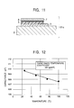
- FIG. 10 is a sectional view showing a temperature-compensating thin-film capacitor of the third embodiment of the present invention.
- a first dielectric thin-film 5 which is deposited on a second dielectric thin-film 4 containing the fluoric polymer as a main component and a protective coating 8 is deposited on and used to cover the first dielectric thin-film 5.
- the same components as the first embodiment have the same reference number as the first embodiment.
- the material of the protective coating 8 is preferably corrosion-resistant against a resist-developing solution and a resist-peeling solution used for forming electrodes, and is preferably selected from a group consisting of SiN x such as Si 3 N 4 , SiO x such as SiO 2 , amorphous SiO x N y , Ti, and the like.
- the thin-film capacitor 31 of the second embodiment has the above structure, hence the thin-film capacitor 31 provides the same effect as the thin-film capacitor 1 of the first embodiment.
- the protective coating 8 is deposited on the first dielectric thin-film 5 containing a fluoric polymer as a main component to cover the first dielectric thin-film 5, so that the first dielectric thin-film 5 is prevented from corrosion which is caused by the resist-developing solution and the resist-peeling solution used for forming electrodes.
- the protective coating 8, the second dielectric thin-film 4, and the first dielectric thin-film 5 are placed between a first electrode layer 3 and a second electrode layer 7.
- the first dielectric thin-film 5 and the protective coating 8 which is deposited thereon may be placed between the first electrode layer 3 and the second electrode layer 7 as shown in FIG. 11.
- a reference numeral 2 in FIG. 11 represents a substrate.
- each capacitor included a dielectric thin-film placed between an upper electrode and a lower electrode which were composed of copper and were deposited on a substrate composed of alumina or glass.
- Each thickness of the upper electrode and the lower electrode was 1,500 nm (15,000 ⁇ ) and the thickness of the dielectric thin-film was 2,000 nm (20,000 ⁇ ).
- the length and width of the upper electrode were controlled within the range of 50 to 1,000 ⁇ m in order to keep the capacitance of the thin-film capacitor at 10 pF.
- the Q factor, the specific inductive capacity, the linear thermal expansion coefficient, the material for composing the thin-film, and the evaluation of each sample is shown in Table 1.
- PTFE represents polytetrafluoroethylene
- PFDA represents a cyclic polymer of perfluorodivinyl ether
- PFA represents a polytetrafluoroethylene-perfluoroalkylvinyl ether copolymer
- FEP represents a tetrafluoroethylene-hexafluoropropylene copolymer
- PCTFE represents polychloro trifluoroethylene
- ETFE represents a tetrafluoroethylene-ethylene copolymer
- ECTFE represents a chlorotrifluoroethylene-ethylene copolymer
- PP represents polypropylene
- PEI represents polyetherimide
- PPS represents polyphenylenesulfide
- SPS represents syndiotactic polystyrene
- PEEK represents polyether ether ketone.
- a material having a specific inductive capacity of 4.0 or less is superior and a material having a linear thermal expansion coefficient of 25 ppm/°C or more is also superior, but a material having a linear thermal expansion coefficient of less than 25 ppm/°C is inferior.
- Table 1 shows that controlling the capacitance-temperature coefficients of the dielectric thin-films of Samples 9 and 10 to negative values is difficult because the linear thermal expansion coefficients thereof are less than 25 ppm/°C.
- controlling the capacitance-temperature coefficients of the dielectric thin-films of Samples 1 to 8 and 11 to 12 in the negative range is possible because the specific inductive capacity and the linear thermal expansion coefficients thereof satisfy the desired conditions.
- the dielectric thin-films of Samples 1 to 8 and 11 to 12 are hardly affected by processing accuracy, hence, the dielectric thin-films have small differences in capacitance.
- the Q factor generally tends to decrease as the frequency increases, the capacitors of Samples 1 to 4, 8 and 11 to 12 have Q factors of 100 or more at a frequency of 1 GHz or more. That is, the capacitors have excellent high frequency characteristics.
- a thin-film capacitor was prepared according to the procedure described below.
- the thin-film capacitor had a first and a second dielectric thin-film placed between electrode layers and had a multilayer structure.
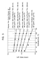
- a capacitance-temperature coefficient, a Q factor at 1 GHz, and a dielectric strength of a thin-film capacitor were measured. The measurement was performed by varying the thickness of the first dielectric thin-film within the range of 50 to 300 nm (500 to 3,000 ⁇ ).
- the capacitance-temperature coefficient was determined according to the slope of the plot of a capacitance (pF) versus temperature (°C) varied in the range of 20 to 120 °C, as shown in FIG. 5.
- the thicknesses of the first dielectric thin-film and the second dielectric thin-film, and the capacitance-temperature coefficient are shown in Table 2.
- the thin-film capacitor was prepared as follows. A copper lower electrode having a thickness of 1,500 nm (15,000 ⁇ ) was deposited on an alumina or glass substrate by sputtering; and then the dielectric thin-film which was composed of SiN x and had a thickness of 300nm (3,000 ⁇ ) was deposited on the lower electrode by PECVD.
- a solution which contains perfluorotributylamine (TFPA) as a solvent and a cyclic polymer of perfluorodivinyl ether was applied onto the second dielectric thin-film by a spin coat method, and then the applied film was cured by (1) curing at 50°C for 2 minutes, (2) curing at 110°C for 2 minutes, and (3) curing at 250°C for 10 minutes, if necessary.
- the first dielectric thin-film composed of the cyclic polymer of perfluorodivinyl ether was formed thereby on the second dielectric thin-film.
- the first dielectric thin-film was etched by 20 nm (200 ⁇ ) from the surface in argon plasma using a dry etcher; a photoresist pattern was formed on the polymer film by photoresist-coating, pre-baking, exposing, developing, and post-baking; the first dielectric thin-film and the second dielectric thin-film were continuously etched with SF 6 or CF 4 by a single process; and then the photoresist was removed. Finally, a copper upper electrode layer having a thickness of 1,500 nm (15,000 ⁇ ) was formed on the first dielectric thin-film by sputtering at room temperature. The dielectric thin-film having a multilayer structure was provided thereby.
- the length and width of the upper electrode were controlled within the range of 50 to 1,000 ⁇ m in order to keep the capacitance of the thin-film capacitor at 10 pF.
- the thin-film capacitor had a Q factor in the range of 210 to 290 at a frequency of 1 GHz and a dielectric strength of 200 V or more.
- the first dielectric thin-film had various Q factors and dielectric strengths according to the thicknesses thereof.
- the SiN x second dielectric thin-film had a linear thermal expansion coefficient of 3 ppm/°C and a specific inductive capacity of 7.0. Also, the thin-film capacitor had a Q factor of 200 at a frequency of 1 GHz when only the second dielectric thin-film was formed between the electrode layers.
- the first dielectric thin-film composed of the cyclic polymer of perfluorodivinyl ether had a linear thermal expansion coefficient of 74 ppm/°C and a specific inductive capacity of 2.1. Also, the thin-film capacitor had a capacitance-temperature coefficient of -677 ppm/°C and a Q factor of 300 at a frequency of 1 GHz when only the first dielectric thin-film was formed between the electrode layers. Thickness of first dielectric thin-film Thickness of second dielectric thin-film Capacitance-temperature coefficient (nm) (nm) (ppm/°C) 50 300 -240 100 300 -360 200 300 -462 300 300 -512
- FIG. 5 and Table 2 show that the capacitance-temperature coefficient of the thin-film capacitor, which comprises the second dielectric thin-film (a SiN x layer) and the first dielectric thin-film (a polymer layer) both placed between the electrodes, is controllable within the range of -240 to -512 ppm/°C.
- the above coefficient is achieved by varying the ratio of the thickness of the first dielectric thin-film to that of the second dielectric thin-film. That is, the thickness of the first dielectric thin-film is varied in the range of 50 to 300 nm when the first dielectric thin-film has a linear thermal expansion coefficient of 74 ppm/°C and a specific inductive capacity of 2.1.
- the thin-film capacitor of this embodiment is suitable to a temperature-compensating electronic device including a varactor diode having a positive capacitance-temperature coefficient.
- FIG. 5 and Table 2 show the following results.
- the thin-film capacitor including only the second dielectric thin-film between the electrodes exhibits a Q factor of 200 at a frequency of 1 GHz
- the thin-film capacitor of this embodiment including the second dielectric thin-film and the first dielectric thin-film which are both placed between the electrodes has a Q factor of 210 or more at a frequency of 1 GHz.
- the relationship between the dimensional difference in processing and the difference in capacitance of a thin-film capacitor were measured while varying the dielectric constant of the copper dielectric thin-film.
- the dimensional difference in processing means the difference between the actual size of a thin-film capacitor and the design size.
- the difference in capacitance is caused by the dimensional difference.
- the dielectric thin-films were placed between the lower electrode and the upper electrode.
- the target sheet capacitance of the thin-film capacitor was 10 pF.
- Cs ⁇ 0 ⁇ ⁇ ⁇ (S/d) wherein ⁇ 0 is 8.854 ⁇ 10 -14 F•cm -1 , S represents the area of the electrodes, d represents the distance between the electrodes, and ⁇ represents the specific inductive capacity.
- the dimensional difference in processing and the difference in capacitance of a thin-film capacitor are shown in Table 3.
- the capacitor included a dielectric thin-film which was composed of ECTFE and had a specific inductive capacity of 2.5, in which the electrode length L was 0.4 mm and the interelectrode distance was 0.3 ⁇ m.
- the dimensional difference in processing and the difference in capacitance of the thin-film capacitor are shown in Table 4.
- the capacitor included a dielectric thin-film which was composed of PPS and had a specific inductive capacity of 4, in which the electrode length L was 0.3 mm and the interelectrode distance was 0.3 ⁇ m.
- the PPS material used in this example had a specific inductive capacity which was within the scope of the present invention, but had a linear thermal expansion coefficient which was outside of the scope of the present invention. Accordingly, the PPS material was measured in order to only investigate effects caused by the specific inductive capacity on the difference in capacitance.
- Table 5 shows the dimensional difference in processing and difference in capacitance of a thin-film capacitor.
- the thin-film capacitor had an electrode length L of 0.02 mm and an interelectrode distance of 0.3 ⁇ m.
- the capacitor included a BaTiO 2 dielectric thin-film having a specific inductive capacity of 1,000.
- the interelectrode distance is the same as that of a thin-film capacitor having a specific inductive capacity of 2.5 or 4.
- Table 6 shows the dimensional difference in processing and difference in capacitance of a thin-film capacitor.
- the thin-film capacitor had an electrode length L of 0.3 mm and an interelectrode distance of 80 ⁇ m.
- the capacitor included a BaTiO 2 dielectric thin-film having a specific inductive capacity of 1,000.
- the electrode area of the thin-film capacitor is the same as that of a thin-film capacitor having a specific inductive capacity of 4.
- the difference in capacitance significantly deviates from a tolerance range, ⁇ 5% of 10 pF, if the dimensional difference in processing is 1 ⁇ m or more, in which a thin-film capacitor includes a dielectric thin-film having a specific inductive capacity of 1,000 and has the same interelectrode distance as that of a thin-film capacitor including a dielectric thin-film having a specific inductive capacity of 2.5 or 4.
- the difference in capacitance is inside the tolerance range if the dimensional difference in processing is 5 ⁇ m or less, in which a thin-film capacitor includes a dielectric thin-film having a specific inductive capacity of 1,000 and has the same electrode area as that of a capacitor including a dielectric thin-film having a specific inductive capacity of 4.
- miniaturization of such a capacitor is difficult because an interelectrode distance is 80 ⁇ m or more.
- the difference in capacitance is inside the tolerance range if the dimensional difference in processing is 5 ⁇ m or less, in which a capacitor comprises a dielectric thin-film having a specific inductive capacity of 2.5 or 4. Also, the interelectrode distance of the thin-film capacitor having a specific inductive capacity of 4 is 1/27 in comparison with that of the thin-film capacitor having a specific inductive capacity of 1,000, wherein the electrode area of both thin-film capacitors is the same.
- the difference in capacitance caused by the dimensional difference in processing is reduced, and miniaturization and thinning of a capacitor is possible if the specific inductive capacity of the dielectric thin-film is 4 or less.
- a thin-film capacitor was prepared according to the procedure described below.
- the thin-film capacitor had a first and a second dielectric thin-film placed between electrode layers and had a multilayer structure.
- a capacitance-temperature coefficient, a Q factor at 1 GHz, and a dielectric strength of a thin-film capacitor were measured.
- the capacitance-temperature coefficient was determined according to the slope of the plot of a capacitance (pF) versus temperature (°C) varied in the range of 20 to 100 °C, as in FIG. 12.
- the thin-film capacitor was prepared as follows. A copper lower electrode having a thickness of 1,500nm (15,000 ⁇ ) was deposited on an alumina or glass substrate by sputtering, and then the SiN x second dielectric thin-film having a thickness of 150nm (1,500 ⁇ ) was deposited on the lower electrode by PECVD.
- a photoresist pattern was formed on the polymer film of the second dielectric thin-film by photoresist-coating, pre-baking, exposing, developing, and post-baking; the first dielectric thin-film and the second dielectric thin-film were continuously etched with SF 6 or CF 4 by a single process; and then the photoresist was removed.
- a copper upper electrode layer having a thickness of 1,500 nm (15,000 ⁇ ) was formed on the first dielectric thin-film by sputtering at room temperature.
- the dielectric thin-film having a multilayer structure was provided thereby.
- the thin-film capacitor having a multilayer structure had a Q factor of 100 at a frequency of 1 GHz, a dielectric strength of 150 V or more, and a capacitance-temperature coefficient of -261 ppm/°C.
- the SiN x second dielectric thin-film had a linear thermal expansion coefficient of 3 ppm/°C and a specific inductive capacity of 7.0. Also, the thin-film capacitor had a Q factor of 200 at a frequency of 1 GHz when only the second dielectric thin-film was formed between the electrode layers.
- the first dielectric thin-film composed of the benzocyclobutene polymer had a linear thermal expansion coefficient of 52 ppm/°C and a specific inductive capacity of 2.7. Also, the thin-film capacitor had a capacitance-temperature coefficient of -380 ppm/°C and a Q factor of 250 at a frequency of 1 GHz when only the first dielectric thin-film was formed between the electrode layers.
- the thin-film capacitor having a capacitance-temperature coefficient of -261 ppm/°C is provided when the capacitor has the second dielectric thin-film composed of SiN x and the first dielectric thin-film composed of the benzocyclobutene polymer which are both placed between electrodes. Accordingly, the thin-film capacitor of this example is applicable to a temperature-compensating circuit of a varactor diode having a positive capacitance-temperature coefficient because the capacitor has a negative capacitance-temperature coefficient.
- the capacitor of this example has a Q factor of 100 or more, which is a large factor.
- a thin-film capacitor was prepared according to the procedure described below.
- the thin-film capacitor had a first and a second dielectric thin-film placed between electrode layers and had a multilayer structure.
- a capacitance-temperature coefficient, a Q factor at 1 GHz, and a dielectric strength of a thin-film capacitor were measured.
- the capacitance-temperature coefficient was determined according to the slope of the plot of a capacitance (pF) versus temperature (°C) varied in the range of 20 to 100 °C, as in FIG. 13.
- the thin-film capacitor was prepared as follows. A copper lower electrode having a thickness of 1,500nm (15,000 ⁇ ) was deposited on an alumina or glass substrate by sputtering, and then the SiN x second dielectric thin-film having a thickness of 150nm (1,500 ⁇ ) was deposited on the lower electrode by PECVD.
- a photoresist pattern was formed on the polymer film of the second dielectric thin-film by photoresist-coating, pre-baking, exposing, developing, and post-baking; the first dielectric thin-film and the second dielectric thin-film were continuously etched with SF 6 or CF 4 by a single process; and then the photoresist was removed.
- a copper upper electrode layer having a thickness of 1,500 nm (15,000 ⁇ ) was formed on the first dielectric thin-film by sputtering at room temperature.
- the dielectric thin-film having a multilayer structure was provided thereby.
- the thin-film capacitor having a multilayer structure had a Q factor of 100 at a frequency of 1 GHz, a dielectric strength of 150 V or more, and a capacitance-temperature coefficient of -238 ppm/°C.
- the second dielectric thin-film composed of SiN x had a linear thermal expansion coefficient of 3 ppm/°C and a specific inductive capacity of 7.0. Also, the second dielectric thin-film had a Q factor of 200 at a frequency of 1 GHz when only the second dielectric thin-film was formed between the electrode layers.
- the first dielectric thin-film composed of the naphthocyclobutene polymer had a linear thermal expansion coefficient of 50 ppm/°C and a specific inductive capacity of 2.75. Also, the first dielectric thin-film had a capacitance-temperature coefficient of -370 ppm/°C and a Q factor of 240 at a frequency of 1 GHz when only the first dielectric thin-film was formed between the electrode layers.
- the thin-film capacitor of this example is applicable to a temperature-compensating circuit of a varactor diode having a positive capacitance-temperature coefficient because the capacitor has a negative capacitance-temperature coefficient.
- the capacitor of this example has a Q factor of 100 or more, which is a large factor.
- a thin-film capacitor was prepared according to the procedure described below.
- the thin-film capacitor had a first and a second dielectric thin-film placed between electrode layers and had a multilayer structure.
- a capacitance-temperature coefficient, a Q factor at 1 GHz, and a dielectric strength of a thin-film capacitor were measured.
- the capacitance-temperature coefficient was determined according to the slope of the plot of a capacitance (pF) versus temperature (°C) varied in the range of 20 to 100 °C, as in FIG. 14.
- the thin-film capacitor was prepared as follows. A copper lower electrode having a thickness of 1,500nm (15,000 ⁇ ) was deposited on an alumina or glass substrate by sputtering, and then the SiN x second dielectric thin-film having a thickness of 150nm (1,500 ⁇ ) was deposited on the lower electrode by PECVD.
- a photoresist pattern was formed on the polymer film of the second dielectric thin-film by photoresist-coating, pre-baking, exposing, developing, and post-baking; the first dielectric thin-film and the second dielectric thin-film were continuously etched with SF 6 or CF 4 by a single process; and then the photoresist was removed.
- a copper upper electrode layer having a thickness of 1,500 nm (15,000 ⁇ ) was formed on the first dielectric thin-film by sputtering at room temperature.
- the dielectric thin-film having a multilayer structure was provided thereby.
- the thin-film capacitor having a multilayer structure had a Q factor of 100 at a frequency of 1 GHz, a dielectric strength of 150 V or more, and a capacitance-temperature coefficient of -243 ppm/°C.
- the second dielectric thin-film composed of SiN x had a linear thermal expansion coefficient of 3 ppm/°C and a specific inductive capacity of 7.0. Also, the second dielectric thin-film had a Q factor of 200 at a frequency of 1 GHz when only the second dielectric thin-film was formed between the electrode layers.
- the first dielectric thin-film composed of the naphthocyclobutene polymer had a linear thermal expansion coefficient of 50 ppm/°C and a specific inductive capacity of 2.8. Also, the first dielectric thin-film had a capacitance-temperature coefficient of -373 ppm/°C and a Q factor of 230 at a frequency of 1 GHz when only the first dielectric thin-film was formed between the electrode layers.
- the above result shows that a thin-film capacitor having a capacitance-temperature coefficient of -243 ppm/°C is provided when the capacitor has the second dielectric thin-film composed of SiN x and the first dielectric thin-film composed of the naphthocyclobutene polymer which are both placed between electrodes. Accordingly, the thin-film capacitor of this example is applicable to a temperature-compensating circuit of a varactor diode having a positive capacitance-temperature coefficient because the capacitor has a negative capacitance-temperature coefficient.
- the capacitor of this example has a Q factor of 100 or more, which is a large factor.
Landscapes
- Engineering & Computer Science (AREA)
- Power Engineering (AREA)
- Microelectronics & Electronic Packaging (AREA)
- Manufacturing & Machinery (AREA)
- Fixed Capacitors And Capacitor Manufacturing Machines (AREA)
- Semiconductor Integrated Circuits (AREA)
Applications Claiming Priority (4)
| Application Number | Priority Date | Filing Date | Title |
|---|---|---|---|
| JP2000389008 | 2000-12-21 | ||
| JP2000389008 | 2000-12-21 | ||
| JP2001254927 | 2001-08-24 | ||
| JP2001254927A JP2002252143A (ja) | 2000-12-21 | 2001-08-24 | 温度補償用薄膜コンデンサ及び電子機器 |
Publications (2)
| Publication Number | Publication Date |
|---|---|
| EP1217637A2 true EP1217637A2 (de) | 2002-06-26 |
| EP1217637A3 EP1217637A3 (de) | 2005-01-26 |
Family
ID=26606293
Family Applications (1)
| Application Number | Title | Priority Date | Filing Date |
|---|---|---|---|
| EP01125397A Withdrawn EP1217637A3 (de) | 2000-12-21 | 2001-10-31 | Temperaturkompensierender Dünnschichtkondensator und Elektronikbauteil |
Country Status (5)
| Country | Link |
|---|---|
| US (1) | US6556421B2 (de) |
| EP (1) | EP1217637A3 (de) |
| JP (1) | JP2002252143A (de) |
| KR (1) | KR100428225B1 (de) |
| CN (1) | CN1198297C (de) |
Cited By (3)
| Publication number | Priority date | Publication date | Assignee | Title |
|---|---|---|---|---|
| DE102004005082A1 (de) * | 2004-02-02 | 2005-08-18 | Infineon Technologies Ag | Kondensator mit einem Dielektrikum aus einer selbstorganisierten Monoschicht einer organischen Verbindung |
| WO2009151694A3 (en) * | 2008-03-13 | 2010-03-04 | Strategic Polymer Sciences, Inc. | Device with a dielectric layer comprising a high energy density polymeric composition |
| CN109166730A (zh) * | 2018-08-28 | 2019-01-08 | 西安交通大学 | 一种宽温高储能的无铅柔性的介电薄膜电容器及其制备方法 |
Families Citing this family (17)
| Publication number | Priority date | Publication date | Assignee | Title |
|---|---|---|---|---|
| US6461886B1 (en) * | 2000-05-13 | 2002-10-08 | Semiconductor Energy Laboratory Co., Ltd. | Method of manufacturing a semiconductor device |
| UA77459C2 (en) * | 2001-11-03 | 2006-12-15 | Thin-film capacitor and a method for producing the capacitor | |
| US20040061990A1 (en) * | 2002-09-26 | 2004-04-01 | Dougherty T. Kirk | Temperature-compensated ferroelectric capacitor device, and its fabrication |
| US7161795B1 (en) * | 2005-09-26 | 2007-01-09 | Ferro Corporation | COG dielectric composition for use with copper electrodes |
| US8223472B1 (en) * | 2008-11-14 | 2012-07-17 | Sandia Corporation | Norbornylene-based polymer systems for dielectric applications |
| JP4905497B2 (ja) * | 2009-04-22 | 2012-03-28 | 株式会社村田製作所 | 電子部品 |
| TW201121786A (en) * | 2009-10-22 | 2011-07-01 | Chi Lin Technology Co Ltd | Hybrid electret |
| US8315032B2 (en) | 2010-07-16 | 2012-11-20 | Ut-Battelle, Llc | High power density capacitor and method of fabrication |
| JP5679167B2 (ja) * | 2010-10-18 | 2015-03-04 | 信越ポリマー株式会社 | フィルムキャパシタ用フィルム |
| GB201212487D0 (en) * | 2012-07-13 | 2012-08-29 | Secr Defence | A device for measuring the hydration level of humans |
| CN103772783A (zh) * | 2013-12-18 | 2014-05-07 | 芜湖万润机械有限责任公司 | 一种电容器用改性聚乙烯等规聚丙烯复合金属化薄膜及其制备方法 |
| KR20160145690A (ko) * | 2014-04-16 | 2016-12-20 | 더 보드 오브 트러스티스 오브 더 리랜드 스탠포드 쥬니어 유니버시티 | 고성능 전자 및 광전자 장치를 위한 극성 엘라스토머 |
| TWI754606B (zh) * | 2014-05-29 | 2022-02-11 | 美商西凱渥資訊處理科技公司 | 用於射頻裝置之溫度補償電路 |
| EP3671780B1 (de) * | 2017-11-15 | 2024-10-09 | Murata Manufacturing Co., Ltd. | Folienkondensator und metallisierte folie |
| US11469761B1 (en) | 2020-09-11 | 2022-10-11 | Mixed-Signal Devices Inc. | CMOS frequency reference circuit with temperature coefficient cancellation |
| US12261596B1 (en) | 2020-09-11 | 2025-03-25 | Mixed-Signal Devices Inc. | Systems and methods for low temperature coefficient capacitors |
| US12085972B1 (en) | 2021-04-01 | 2024-09-10 | Mixed-Signal Devices Inc. | Sampled band-gap reference voltage generators |
Family Cites Families (19)
| Publication number | Priority date | Publication date | Assignee | Title |
|---|---|---|---|---|
| US3949280A (en) * | 1975-02-18 | 1976-04-06 | Mitsumi Electric Co., Ltd. | Miniature variable capacitor and method of manufacture |
| JPS5873908A (ja) * | 1981-10-28 | 1983-05-04 | ティーディーケイ株式会社 | 高周波用誘電体磁器組成物 |
| WO1984003003A1 (fr) * | 1983-01-31 | 1984-08-02 | Nippon Soda Co | Dielectrique a film mince et son procede de production |
| JPS63110618A (ja) | 1986-10-28 | 1988-05-16 | 沖電気工業株式会社 | 積層型マイクロ波用誘電体磁器組成物 |
| EP0393271A1 (de) * | 1987-08-08 | 1990-10-24 | The Standard Oil Company | Dünnschichtüberzüge aus Fluorpolymer und Verfahren zu ihrer Herstellung durch Plasmapolymerisation |
| DE68906219T2 (de) | 1988-08-25 | 1993-08-05 | Matsushita Electric Ind Co Ltd | Duennfilmkapazitaet und verfahren zur herstellung einer integrierten hybridmikrowellenschaltung. |
| US5088003A (en) * | 1989-08-24 | 1992-02-11 | Tosoh Corporation | Laminated silicon oxide film capacitors and method for their production |
| JPH03252160A (ja) * | 1990-02-28 | 1991-11-11 | Nec Corp | コンデンサ、コンデンサネットワーク及び抵抗―コンデンサネットワーク |
| US5311406A (en) * | 1991-10-30 | 1994-05-10 | Honeywell Inc. | Microstrip printed wiring board and a method for making same |
| US5723171A (en) * | 1992-10-23 | 1998-03-03 | Symetrix Corporation | Integrated circuit electrode structure and process for fabricating same |
| JPH08115851A (ja) * | 1994-10-14 | 1996-05-07 | Ngk Spark Plug Co Ltd | 薄膜コンデンサ付きセラミック基板および その製造方法 |
| JP3475976B2 (ja) * | 1995-01-13 | 2003-12-10 | 出光石油化学株式会社 | コンデンサ |
| EP0749134B1 (de) | 1995-06-16 | 2002-10-02 | AT&T IPM Corp. | TiO2 dotiertes, Ta2O5 enthaltendes dielektrisches Material und dieses enthaltende Bauteile |
| AU2923397A (en) * | 1996-04-18 | 1997-11-07 | California Institute Of Technology | Thin film electret microphone |
| US5965273A (en) * | 1997-01-31 | 1999-10-12 | Hoechst Celanese Corporation | Polymeric compositions having a temperature-stable dielectric constant |
| US6153525A (en) * | 1997-03-13 | 2000-11-28 | Alliedsignal Inc. | Methods for chemical mechanical polish of organic polymer dielectric films |
| JPH11214250A (ja) * | 1998-01-28 | 1999-08-06 | Kuraray Co Ltd | デバイスとこれを実装した実装回路基板 |
| US6324048B1 (en) * | 1998-03-04 | 2001-11-27 | Avx Corporation | Ultra-small capacitor array |
| US6154311A (en) * | 1998-04-20 | 2000-11-28 | Simtek Hardcoatings, Inc. | UV reflective photocatalytic dielectric combiner having indices of refraction greater than 2.0 |
-
2001
- 2001-08-24 JP JP2001254927A patent/JP2002252143A/ja not_active Withdrawn
- 2001-10-31 EP EP01125397A patent/EP1217637A3/de not_active Withdrawn
- 2001-12-19 US US10/028,543 patent/US6556421B2/en not_active Expired - Fee Related
- 2001-12-20 KR KR10-2001-0081832A patent/KR100428225B1/ko not_active Expired - Fee Related
- 2001-12-21 CN CNB011449012A patent/CN1198297C/zh not_active Expired - Fee Related
Cited By (5)
| Publication number | Priority date | Publication date | Assignee | Title |
|---|---|---|---|---|
| DE102004005082A1 (de) * | 2004-02-02 | 2005-08-18 | Infineon Technologies Ag | Kondensator mit einem Dielektrikum aus einer selbstorganisierten Monoschicht einer organischen Verbindung |
| DE102004005082B4 (de) * | 2004-02-02 | 2006-03-02 | Infineon Technologies Ag | Kondensator mit einem Dielektrikum aus einer selbstorganisierten Monoschicht einer organischen Verbindung und Verfahren zu dessen Herstellung |
| US7202547B2 (en) | 2004-02-02 | 2007-04-10 | Infineon Technologies, Ag | Capacitor with a dielectric including a self-organized monolayer of an organic compound |
| WO2009151694A3 (en) * | 2008-03-13 | 2010-03-04 | Strategic Polymer Sciences, Inc. | Device with a dielectric layer comprising a high energy density polymeric composition |
| CN109166730A (zh) * | 2018-08-28 | 2019-01-08 | 西安交通大学 | 一种宽温高储能的无铅柔性的介电薄膜电容器及其制备方法 |
Also Published As
| Publication number | Publication date |
|---|---|
| KR100428225B1 (ko) | 2004-04-28 |
| CN1198297C (zh) | 2005-04-20 |
| CN1360323A (zh) | 2002-07-24 |
| EP1217637A3 (de) | 2005-01-26 |
| KR20020050734A (ko) | 2002-06-27 |
| JP2002252143A (ja) | 2002-09-06 |
| US20020122285A1 (en) | 2002-09-05 |
| US6556421B2 (en) | 2003-04-29 |
Similar Documents
| Publication | Publication Date | Title |
|---|---|---|
| EP1217637A2 (de) | Temperaturkompensierender Dünnschichtkondensator und Elektronikbauteil | |
| US5172304A (en) | Capacitor-containing wiring board and method of manufacturing the same | |
| US7875956B2 (en) | Multi-level thin film capacitor on a ceramic substrate and method of manufacturing the same | |
| KR100505305B1 (ko) | 캐패시터를구비한물품 | |
| US6477036B2 (en) | Temperature compensating thin-film capacitor | |
| US8569142B2 (en) | Multi-level thin film capacitor on a ceramic substrate and method of manufacturing the same | |
| WO2001067465A2 (en) | Lead zirconate titanate dielectric thin film composites on metallic foils | |
| WO2008138127A1 (en) | Systems and methods for a thin film capacitor having a composite high-k thin film stack | |
| Pushkar et al. | Thin-film capacitors for packaged electronics | |
| US6482527B1 (en) | Pyrochlore thin films and process for making | |
| Ma et al. | Chemical solution deposition of ferroelectric lead lanthanum zirconate titanate films on base-metal foils | |
| US7079373B2 (en) | Dielectric sheet, method for fabricating the dielectric sheet, printed circuit and patch antenna using the dielectric sheet, and method for fabricating the printed circuit | |
| Hyun et al. | Frequency and temperature dependence of dielectric constant of epoxy/BaTiO 3 composite embedded capacitor films (ECFs) for organic substrate | |
| Ulrich | Matching embedded capacitor dielectrics to applications | |
| US6872468B1 (en) | Peelable circuit board foil | |
| Imanaka et al. | Embedded capacitor technology using aerosol deposition | |
| EP1187184A2 (de) | Temperaturkompensierender Düunnfilmkondensator | |
| US3271192A (en) | Capacitors and process for making same | |
| US4374179A (en) | Plasma polymerized ethane for interlayer dielectric | |
| Hyun et al. | A study on the temperature dependence of epoxy/BaTiO3 composite embedded capacitor films | |
| Potrepka et al. | Sputtered Platinum (Pt) Electrode Development for Lead Zirconate Titanate (PZT) Piezoelectric Microelectromechanical Systems (MEMS) Devices | |
| Hoffmann et al. | Graded dielectric thin films prepared by chemical solution deposition | |
| Noda et al. | Comparison of BST film microwave tunable devices based on (100) and (111) MgO substrates | |
| KR20110001688A (ko) | 유전체 세라믹스 후막 및 그 제조방법 | |
| JP3622773B2 (ja) | セラミック電子部品 |
Legal Events
| Date | Code | Title | Description |
|---|---|---|---|
| PUAI | Public reference made under article 153(3) epc to a published international application that has entered the european phase |
Free format text: ORIGINAL CODE: 0009012 |
|
| AK | Designated contracting states |
Kind code of ref document: A2 Designated state(s): AT BE CH CY DE DK ES FI FR GB GR IE IT LI LU MC NL PT SE TR |
|
| AX | Request for extension of the european patent |
Free format text: AL;LT;LV;MK;RO;SI |
|
| PUAL | Search report despatched |
Free format text: ORIGINAL CODE: 0009013 |
|
| AK | Designated contracting states |
Kind code of ref document: A3 Designated state(s): AT BE CH CY DE DK ES FI FR GB GR IE IT LI LU MC NL PT SE TR |
|
| AX | Request for extension of the european patent |
Extension state: AL LT LV MK RO SI |
|
| 17P | Request for examination filed |
Effective date: 20050307 |
|
| AKX | Designation fees paid |
Designated state(s): DE FI FR GB |
|
| 17Q | First examination report despatched |
Effective date: 20060901 |
|
| STAA | Information on the status of an ep patent application or granted ep patent |
Free format text: STATUS: THE APPLICATION IS DEEMED TO BE WITHDRAWN |
|
| 18D | Application deemed to be withdrawn |
Effective date: 20070112 |