EP1220101B1 - Verfahren und Vorrichtung zum Schutz gegen unbefugte Benutzung eines integrierten Schaltkreises - Google Patents
Verfahren und Vorrichtung zum Schutz gegen unbefugte Benutzung eines integrierten Schaltkreises Download PDFInfo
- Publication number
- EP1220101B1 EP1220101B1 EP01126122A EP01126122A EP1220101B1 EP 1220101 B1 EP1220101 B1 EP 1220101B1 EP 01126122 A EP01126122 A EP 01126122A EP 01126122 A EP01126122 A EP 01126122A EP 1220101 B1 EP1220101 B1 EP 1220101B1
- Authority
- EP
- European Patent Office
- Prior art keywords
- time delay
- integrated circuit
- circuit
- capacitor
- active
- Prior art date
- Legal status (The legal status is an assumption and is not a legal conclusion. Google has not performed a legal analysis and makes no representation as to the accuracy of the status listed.)
- Expired - Lifetime
Links
Images



Classifications
-
- G—PHYSICS
- G06—COMPUTING OR CALCULATING; COUNTING
- G06F—ELECTRIC DIGITAL DATA PROCESSING
- G06F21/00—Security arrangements for protecting computers, components thereof, programs or data against unauthorised activity
- G06F21/70—Protecting specific internal or peripheral components, in which the protection of a component leads to protection of the entire computer
- G06F21/71—Protecting specific internal or peripheral components, in which the protection of a component leads to protection of the entire computer to assure secure computing or processing of information
- G06F21/75—Protecting specific internal or peripheral components, in which the protection of a component leads to protection of the entire computer to assure secure computing or processing of information by inhibiting the analysis of circuitry or operation
- G06F21/755—Protecting specific internal or peripheral components, in which the protection of a component leads to protection of the entire computer to assure secure computing or processing of information by inhibiting the analysis of circuitry or operation with measures against power attack
-
- G—PHYSICS
- G06—COMPUTING OR CALCULATING; COUNTING
- G06F—ELECTRIC DIGITAL DATA PROCESSING
- G06F2221/00—Indexing scheme relating to security arrangements for protecting computers, components thereof, programs or data against unauthorised activity
- G06F2221/21—Indexing scheme relating to G06F21/00 and subgroups addressing additional information or applications relating to security arrangements for protecting computers, components thereof, programs or data against unauthorised activity
- G06F2221/2143—Clearing memory, e.g. to prevent the data from being stolen
Definitions
- the present invention relates to a method of protecting an integrated circuit against piracy, at least during execution by the circuit of operations involving the reading of confidential data stored in the integrated circuit.
- the present invention also relates to an integrated circuit comprising at least one memory in which confidential data is stored, calculation means capable of reading the confidential data stored in the memory, and a protection device against the piracy of these confidential data.
- the cryptographic algorithm is generally executed by a wired logic circuit, or cryptographic co-processor, which is assigned a secret key or cryptographic key, which is stored in a zone protected from the memory of the integrated circuit. It is therefore essential to guarantee absolute protection of this secret key because the cryptography algorithms implemented in the authentication procedures are in themselves known and only the secret key guarantees the inviolability of the authentication procedure.
- Such a method relies on a correlation of samples of current consumed with a mathematical model of the cryptography circuit and hypotheses on the value of the secret key.
- the correlation makes it possible to eliminate the continuous part of the consumed current and to highlight consumption peaks which are indicative of the operations carried out by the cryptography circuit and the value of the confidential data. With such a method, it is enough to acquire about 1000 samples to obtain a secret key type DES.
- EP 1022683 thus describes a method of disconnecting the power source of an encryption apparatus when confidential operations are performed.
- the present invention aims to provide additional protection to integrated circuits designed to handle confidential information, especially those fitted to smart cards.
- this method further comprises a step performed by the integrated circuit if the sequence of predetermined processing has been executed normally, consisting of deactivating the timer.
- this method also comprises a step executed by the integrated circuit if the timer is detected active, consisting in modifying the value of a counter in a protected area of a non-volatile memory, comparing the value of this counter to a predefined threshold, and carry out a protection treatment of confidential data stored in memories of the integrated circuit if the value of the counter reaches the predefined threshold.
- said protection process consists in erasing the confidential data of the memories of the integrated circuit.
- said protection treatment consists of erasing a secret code stored in a memory of the integrated circuit.
- said protection treatment consists of erasing all memories of the integrated circuit.
- the integrated circuit Before executing a calculation of a sequence of a predefined number of calculations, the integrated circuit preferably detects the state of a respective timer, each calculation being respectively associated with a delay, it controls the activation of the delay associated if it is not active, and it hangs if the associated timer is active.
- the invention also relates to an integrated circuit protected against piracy, characterized in that it comprises at least one timing circuit comprising means for activating a timer designed to remain in the active state as long as the circuit is under voltage and for a predetermined time if the circuit is de-energized, means for inactivating the timer, and means for detecting the active or inactive state of the timer; the integrated circuit further comprising means for reading the state of the timer, and to lock at predefined times if the timer is in the active state.
- this integrated circuit further comprises means for deactivating the delay following a normal execution of a predetermined processing sequence.
- each delay circuit furthermore comprises means for detecting the presence of the supply voltage, and means for authorizing the activation or inactivation of the delay when the supply voltage is detected present for a predetermined duration.
- this integrated circuit comprises several delay circuits, each delay circuit being associated with a calculation performed by the integrated circuit, the integrated circuit comprising means for, before each calculation, determine the state of the timer associated with the calculation, activate the associated timer if it is not active and lock if the associated timer is active.
- the capacitor discharge control means are designed to discharge the capacitor faster than when the circuit is de-energized.
- this integrated circuit comprises a MOS transistor having very low leakage currents, which is associated with the capacitor so that it only discharges by these leakage currents, when the circuit integrated is off.
- FIG. 1 schematically represents the conventional architecture of an integrated circuit 1 for a smart card.
- This integrated circuit 1 comprises a central processing unit 2, for example of the microprocessor or microcontroller type, a link unit 7 to be able to communicate with or without contact with an external terminal 10, a cryptography circuit 6 and memories 4, namely a read-only memory ROM in which is stored the operating system of the central unit 2, a random access memory RAM for storing temporary data, and a programmable memory and erasable, for example of the EEPROM type, for storing one or more application programs.
- the central unit 2, the memories 4, the cryptography circuit 6 and the linking unit 7 are interconnected by a common data bus 3.
- a secret key used by the cryptographic circuit 6 is stored in a protected area of the ROM or EEPROM.
- the integrated circuit may also include a countermeasure circuit 8 designed to scramble a DPA analysis.
- the integrated circuit 1 also comprises a delay circuit 5 to resist more effectively a DPA type attack.
- this circuit 5 comprises a delay circuit, which comprises an nMOS transistor M1 advantageously designed so as to have a very weak drain-source leakage current, that is to say a perimeter and a drain surface. minimum.
- the drain of this transistor is connected to ground via another nMOS transistor 27 whose gate is connected to a Dchrg discharge control input.
- the drain of the transistor M1 is also connected via a diode D1 mounted in reverse to the drain of a pMOS transistor 24 whose source is connected to the voltage source V dd .
- the gate of transistor 24 is connected to the output of an inverter 25 whose input is connected to the output of an OR gate 23.
- This OR gate 23 has a first input connected to the load control input Chrg of the circuit 5, and a second input connected to the output Q of the circuit 5. In this way, if the output Q or the load control Chrg is at logic level 1, the source of the transistor is placed at logic level 1. Conversely, if Q and Chrg are at logic level 0, the drain of transistor M1 is isolated by diode D1 which is then blocked.
- This diode is preferably a box type diode, so to be isolated from the substrate (that is to say the mass) on which the transistor M1 is formed, to reduce the leakage currents.
- each inverter stage comprises a pMOS transistor 28, 30 and an nMOS transistor 29, 31, connected in series between the voltage source V dd and the ground.
- the transistors 28 to 31 are made so that a very low voltage across the capacitor makes it possible to obtain a logic level 1 at the output Q.
- the gate of the transistor M1 is connected to the output of an AND gate 22 whose inputs are respectively connected to a circuit 32 for detecting the supply voltage V dd and to the output of an OR gate 21.
- the OR gate 21 comprises three input channels, namely a first channel connected to the Q output, a second channel connected to the loading control input CHG, and a third channel connected to the DCHG unloading control.
- FIG. 2a shows in detail the circuit 32 for detecting the supply voltage V dd .
- This circuit comprises two pMOS transistors 35, 36 mounted in a diode (gate connected to the drain), these two transistors being connected in series between the voltage source V dd and the drain of an nMOS transistor 37 whose gate is connected to the source voltage V dd and the source is connected to ground, in order to play the role of resistance.
- the junction point between the transistors 36 and 37 is connected to a first inverter stage comprising a pMOS transistor 38 whose source is at the potential V dd and a nMOS transistor 39 whose source is grounded, this junction point being connected to the grids of the two transistors 38 and 39.
- junction point between the drains of the transistors 38 and 39 is connected to a capacitor 40 whose other terminal is grounded, and to a second inverter stage comprising a pMOS transistor 41 whose source is at the potential V dd , and a nMOS transistor 42 whose source is grounded, the junction point of the drains of the two transistors 41, 42 providing the output signal Enable of the circuit 32.
- the assembly consisting of the capacitor 40 and the last inverter stage with transistors 41 and 42 functions as a delay line.
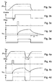
- circuit 5 The operation of the circuit 5 is now explained in more detail with reference to FIGS. 3 and 4 giving as a function of time the shape of different signals of the integrated circuit 1.
- the processing unit 2 sends a pulse to the charge input Chrg of the circuit 5 (curve of FIG. 3c), the Enable signal being in the high state.
- the output of the OR gate 21 goes high, as well as the output of the AND gate 22.
- a voltage is then applied to the gate of the transistor M1.
- the output of the OR gate 23 goes high, which turns on the transistor 24.
- the supply voltage V dd of the circuit is therefore applied to the drain of the transistor M1 which is then conducting, the transistor 27 being blocked (Dchrg discharge control at 0), isolating the drain of the transistor M1 from the ground.
- capacitor C is charged as shown in the curve of Figure 3d.
- the transistor 30 is unblocked, placing the output Q at the logic level 1 (curve of FIG. ) which then takes over the load pulse to keep transistor M1 on.
- the charge control pulse is therefore chosen so wide that the voltage across the capacitor C reaches at least the value V TH .
- the Enable signal goes low, and the output of the AND gate 22 goes low, which blocks the transistor M1.
- the capacitor C is no longer under voltage and discharges through the drain of the transistor M1 (leakage current of the drain-substrate diode of the transistor).
- the output Q follows the supply voltage V dd and therefore falls to 0.
- the time ⁇ t corresponding to the time constant of the capacitor discharge circuit has not elapsed, the voltage across the capacitor C remains greater than the threshold voltage V TH . Consequently, as shown in FIGS. 4a to 4d, any re-energization of the circuit before the time ⁇ t has elapsed causes the transistors 28 and 30 to be energized, and thus the recovery of the Q output and automatic recharging. capacitor C.
- the time constant ⁇ t is the time during which the integrated circuit 1 must be de-energized for the capacitor C to be discharged.
- the capacitor C slowly discharges because of the very low leakage currents that appear through the transistor M1. Therefore, even if the capacitance of the capacitor C is very small, of the order of a few pF, the voltage across the capacitor remains greater than the switching threshold of the inverter stages during the duration ⁇ t.
- C may be 10 pF, ⁇ V 2 V and I 10 pA.
- the time constant ⁇ t is 2 s.
- the time constant can reach 5 s.
- the processing unit 2 sends a pulse to the Dchrg discharge input, the transistor 27 becomes on, which places the drain of the transistor M1 to ground and thus the capacitor C is discharged then in a virtually instantaneous manner, the two transistors M1 and 27 having a low resistance in the on state.
- the transistor 28 becomes on, while the transistor 29 is blocked.
- the transistor 30 then locks in turn, while the transistor 31 is unblocked, placing the Q output output to the ground so that it goes to logic 0.
- the width of the Dchrg discharge control pulse must also be greater than the discharge time of the capacitor C through the transistors M1 and 27, up to the value V TH . It should be noted that the discharge command is applied to the OR gate 21 to ensure that the capacitor C fully discharges. Without this arrangement, the discharge of the capacitor could be stopped as soon as the voltage thereof returns below the voltage V TH , moment at which the signal Q goes back to the low level, which would block the door 21 and therefore the transistor M1.
- FIG. 5a shows the evolution of the voltage V dd during a transaction established with the integrated circuit.
- the reset signal in FIG. 5b changes from logic level 0 to logic level 1, which triggers initialization processing by processing unit 2, then a series of n calculations.
- authentication as can be seen in Figure 5c which represents the activity of the CPU 2.
- the CPU goes into session normal to execute the transaction requested by the terminal.
- the Q output (curve of Figure 5d) is low when the circuit is turned on.
- the circuit 5 is controlled at time t1 by the processing unit 2 which sends a pulse to the input Chrg, so as to trigger the charging of the capacitor C, and therefore to make the Q output go high, the Enable signal is high.
- the output Q goes high, which then keeps the gate and source voltage of the transistor M1 high. Capacitor C therefore remains charged and signal Q is kept high.
- the central unit 2 controls the discharge of the capacitor C by sending a pulse on the Dchrg discharge command, which makes the output Q return to the low level at time t2.
- the CPU 2 detects an abnormal operation revealing an attempted hacking, it does not control the discharge of the capacitor and hangs, for example in a waiting loop (FIGS. , 5f).
- the central unit 2 which executes the initialization procedure, detects that the signal Q is still at the high level, indicating that the capacitor C is not completely discharged and hangs ( Figure 6c).
- the central unit 2 increments a blocking counter stored in the EEPROM memory and definitively blocks when the value of the counter reaches or exceeds a certain threshold predefined.
- the definitive blocking of the integrated circuit may for example consist of erasing the secret key stored in the EEPROM memory, or more generally, erasing all the confidential data stored in this memory, or still all the content of it.
- transistor M1 It is furthermore possible to connect the drain of transistor M1 to an nMOS transistor 26 whose gate is connected to a test control input and whose source is connected to a circuit 33 comprising a plurality of nMOS transistors in parallel between the source. of the transistor 26 and the ground, these transistors being mounted in blocked mode (grid connected to ground).
- These transistors are of the same size as the transistor M1, so that the leakage current that discharges the capacitance C is n times greater than that of M1, where n is the number of transistors of the circuit 33.
- test command must be made sufficiently inaccessible not to be activated by potential hackers.
- each calculation sequence comprises a command for reading the value of the output signal Qi of the delay circuit 5 associated with it, and then, if this signal is at the low level, a load control of the capacitor of this circuit, so as to pass the signal Qi high as shown in Figures 7b to 7d.
- the processing unit 2 detects it by reading the value of the signal Qi corresponding to the calculation sequence, and locks.
Landscapes
- Engineering & Computer Science (AREA)
- Physics & Mathematics (AREA)
- Computer Hardware Design (AREA)
- Theoretical Computer Science (AREA)
- Mathematical Physics (AREA)
- Computer Security & Cryptography (AREA)
- Software Systems (AREA)
- General Engineering & Computer Science (AREA)
- General Physics & Mathematics (AREA)
- Storage Device Security (AREA)
- Semiconductor Integrated Circuits (AREA)
Claims (15)
- Verfahren zum Schutz gegen unbefugter Benutzung eines integrierten Schaltkreises, dadurch gekennzeichnet, dass es die von dem integrierten Schaltkreis (1) vor einer vorbestimmten Sequenz von Behandlungen durchgeführten Schritte aufweist, die darin bestehen, nacheinander:- den Zustand mindestens einer Verzögerung (5) zu erfassen,- das Auslösen der Verzögerung (5) zu veranlassen, wenn diese nicht aktiv ist, und- sich zu blockieren, wenn die Verzögerung aktiv ist.
- Verfahren nach Anspruch 1, dadurch gekennzeichnet, dass es ferner einen Schritt aufweist, der von dem integrierten Schaltkreis (1) ausgeführt wird, wenn die Sequenz vorbestimmter Behandlungen normal ausgeführt wurde, der im Deaktivieren der Verzögerung (5) besteht.
- Verfahren nach Anspruch 1 oder 2, dadurch gekennzeichnet, dass es ferner einen Schritt aufweist, der von dem integrierten Schaltkreis (1) ausgeführt wird, wenn die Verzögerung (5) als aktiv erfasst wird, der darin besteht, den Wert eines Zählers in einer geschützten Zone eines nicht flüchtigen Speichers (EEPROM) zu ändern, den Wert dieses Zählers mit einem vorbestimmten Schwellenwert zu vergleichen und eine Verarbeitung zum Schutz vertraulicher Daten auszuführen, die in Speichern des integrierten Schaltkreises gespeichert sind, wenn der Wert des Zählers einen vorbestimmten Schwellenwert erreicht.
- Verfahren nach Anspruch 3, dadurch gekennzeichnet, dass die Schutzverarbeitung darin besteht, die vertraulichen Daten der Speicher (4) des integrierten Schaltkreises zu löschen.
- Verfahren nach Anspruch 3, dadurch gekennzeichnet, dass die Schutzverarbeitung darin besteht, einen Geheimcode in einem Speicher (4) des integrierten Schaltkreises (1) zu löschen.
- Verfahren nach Anspruch 3, dadurch gekennzeichnet, dass die Schutzverarbeitung darin besteht, alle Speicher (4) des integrierten Schaltkreises (1) zu löschen.
- Verfahren nach einem der vorhergehenden Ansprüche 1 bis 4, dadurch gekennzeichnet, dass der integrierte Schaltkreis (1) vor dem Ausführen einer Berechnung einer Sequenz mit einer vorbestimmten Anzahl von Berechnungen den Zustand einer jeweiligen Verzögerung (5) erfasst, wobei jede Berechnung jeweils mit einer Verzögerung (5) verbunden ist, dass er das Aktivieren der dazugehörenden Verzögerung befiehlt, wenn diese nicht aktiv ist, und sich blockiert, wenn die dazugehörende Verzögerung aktiv ist.
- Integrierter Schaltkreis, der gegen ungefugte Benutzung geschützt ist, dadurch gekennzeichnet, dass er mindestens einen Verzögerungsschaltkreis (5) aufweist, der Mittel zum Aktivieren (Charg) einer Verzögerung aufweist, die konzipiert sind, um im aktiven Zustand zu bleiben, solange an dem Schaltkreis (5) Spannung anliegt, und während einer vorbestimmten Dauer, wenn der Schaltkreis spannungsfrei ist, Mittel zum Deaktivieren (Dcharg) der Verzögerung sowie Mittel (Q) zum Erfassen des aktiven oder inaktiven Zustands der Verzögerung, wobei der integrierte Schaltkreis (1) ferner Mittel aufweist, um den Zustand der Verzögerung zu lesen und sich in vorbestimmten Augenblicken zu blockieren, wenn die Verzögerung im aktiven Zustand ist.
- Integrierter Schaltkreis nach Anspruch 8, dadurch gekennzeichnet, dass er ferner Mittel zum Deaktivieren der Verzögerung im Anschluss an ein normales Ausführen einer vorbestimmten Sequenz von Verarbeitungen aufweist.
- Integrierter Schaltkreis nach Anspruch 8 oder 9, dadurch gekennzeichnet, dass jeder Verzögerungsschaltkreis (5) ferner Mittel (32) aufweist, um die Gegenwart der Versorgungsspannung zu erfassen, sowie Mittel (22), um das Aktivieren oder das Deaktivieren der Verzögerung zu gestatten, wenn die Versorgungsspannung während einer vorbestimmten Dauer als gegenwärtig erfasst wird.
- Integrierter Schaltkreis nach einem der Ansprüche 8 bis 10, dadurch gekennzeichnet, dass er mehrere Verzögerungsschaltkreise (5) aufweist, wobei jeder Verzögerungsschaltkreis mit einer Berechnung verbunden ist, die von dem integrierten Schaltkreis (1) ausgeführt wird, wobei der integrierte Schaltkreis Mittel aufweist, um vor jeder Berechnung den Zustand der zu der Berechnung gehörenden Verzögerung zu bestimmen, die dazugehörende Verzögerung zu aktivieren, wenn diese nicht aktiv ist, und sich zu blockieren, wenn die dazugehörende Verzögerung aktiv ist.
- Integrierter Schaltkreis nach einem der Ansprüche 8 bis 11, dadurch gekennzeichnet, dass jeder Verzögerungsschaltkreis (5) einen Kondensator (C) aufweist, der verbunden ist mit:- einem Entladeschaltkreis (M1), der so konzipiert ist, dass sich der Kondensator (C) langsam entlädt, wenn der Schaltkreis spannungsfrei ist,- einem Schaltkreis (28 bis 30) zum Erfassen der Ladung des Kondensators (C),- Mitteln zum Steuern des Ladens des Kondensators (C) und- Mitteln zum Steuern des Entladens des Kondensators.
- Integrierter Schaltkreis nach Anspruch 12, dadurch gekennzeichnet, dass die Steuermittel (27) der Entladung des Kondensators (C) konzipiert sind, um den Kondensator schneller zu entladen als wenn der Schaltkreis spannungsfrei ist.
- Integrierter Schaltkreis nach einem der Ansprüche 8 bis 13, dadurch gekennzeichnet, dass er einen MOS-Transistor (M1) aufweist, der sehr geringe Leckströme aufweist, der mit dem Kondensator (C) so verbunden ist, dass sich dieser nur durch diese Leckströme entlädt, wenn der integrierte Schaltkreis (1) spannungsfrei ist.
- Integrierter Schaltkreis nach einem der Ansprüche 8 bis 14, dadurch gekennzeichnet, dass er einen Testschaltkreis (33) aufweist, der von einem Testbefehl gesteuert wird, um die Dauer der Verzögerung zu verringern.
Applications Claiming Priority (2)
| Application Number | Priority Date | Filing Date | Title |
|---|---|---|---|
| FR0017261A FR2819070B1 (fr) | 2000-12-28 | 2000-12-28 | Procede et dispositif de protection conte le piratage de circuits integres |
| FR0017261 | 2000-12-28 |
Publications (2)
| Publication Number | Publication Date |
|---|---|
| EP1220101A1 EP1220101A1 (de) | 2002-07-03 |
| EP1220101B1 true EP1220101B1 (de) | 2007-05-30 |
Family
ID=8858377
Family Applications (1)
| Application Number | Title | Priority Date | Filing Date |
|---|---|---|---|
| EP01126122A Expired - Lifetime EP1220101B1 (de) | 2000-12-28 | 2001-11-03 | Verfahren und Vorrichtung zum Schutz gegen unbefugte Benutzung eines integrierten Schaltkreises |
Country Status (4)
| Country | Link |
|---|---|
| US (1) | US7146509B2 (de) |
| EP (1) | EP1220101B1 (de) |
| DE (1) | DE60128646T2 (de) |
| FR (1) | FR2819070B1 (de) |
Families Citing this family (15)
| Publication number | Priority date | Publication date | Assignee | Title |
|---|---|---|---|---|
| FR2786006B1 (fr) * | 1998-11-17 | 2001-10-12 | Schlumberger Systems & Service | Dispositif pour la limitation de fraudes dans une carte a circuit integre |
| GB0221240D0 (en) * | 2002-09-13 | 2002-10-23 | Koninkl Philips Electronics Nv | Current source for cryptographic processor |
| FR2844896A1 (fr) * | 2002-09-19 | 2004-03-26 | St Microelectronics Sa | Alimentation d'un circuit de traitement asynchrone de donnees |
| KR100528464B1 (ko) * | 2003-02-06 | 2005-11-15 | 삼성전자주식회사 | 스마트카드의 보안장치 |
| JP2004361986A (ja) * | 2003-04-08 | 2004-12-24 | Sharp Corp | スクランブル回路 |
| US20050071656A1 (en) * | 2003-09-25 | 2005-03-31 | Klein Dean A. | Secure processor-based system and method |
| DE10360998B4 (de) | 2003-12-23 | 2008-09-04 | Infineon Technologies Ag | Schutz von Chips gegen Attacken |
| EP1612639A1 (de) * | 2004-06-30 | 2006-01-04 | ST Incard S.r.l. | Methode zum Feststellen und zum Ergreifen von Gegenmassnahmen gegen mögliche Angriffe auf Sicherheitsoperationen die von einer Kryptografischen Karte ausgeführt werden |
| US20090049548A1 (en) * | 2005-10-24 | 2009-02-19 | Nxp B.V. | Semiconductor Device and Method For Preventing Attacks on the Semiconductor Device |
| FR2926382B1 (fr) * | 2008-01-11 | 2010-02-26 | Proton World Internat Nv | Hierarchisation de cles cryptographiques dans un circuit electronique |
| CN103605936A (zh) | 2008-06-24 | 2014-02-26 | Nds有限公司 | 集成电路内的安全 |
| BR112012007143A2 (pt) * | 2009-09-29 | 2016-08-23 | NagraID Security SA | dispositivo eletrônico portátil, particularmente um cartão eletrônico, fornecido com um interruptor óptico |
| DE102010044687A1 (de) * | 2010-09-08 | 2012-03-08 | Giesecke & Devrient Gmbh | Portabler Datenträger mit Fehlbedienungszähler |
| JP5776927B2 (ja) * | 2011-03-28 | 2015-09-09 | ソニー株式会社 | 情報処理装置及び方法、並びにプログラム |
| US11621036B2 (en) * | 2020-07-14 | 2023-04-04 | Taiwan Semiconductor Manufacturing Company, Ltd. | Method of operating an integrated circuit and integrated circuit |
Family Cites Families (45)
| Publication number | Priority date | Publication date | Assignee | Title |
|---|---|---|---|---|
| US4317180A (en) * | 1979-12-26 | 1982-02-23 | Texas Instruments Incorporated | Clocked logic low power standby mode |
| JPH0616607B2 (ja) * | 1983-01-12 | 1994-03-02 | キヤノン株式会社 | 光通信装置 |
| GB2182176B (en) * | 1985-09-25 | 1989-09-20 | Ncr Co | Data security device for protecting stored data |
| US4742215A (en) * | 1986-05-07 | 1988-05-03 | Personal Computer Card Corporation | IC card system |
| US4882752A (en) * | 1986-06-25 | 1989-11-21 | Lindman Richard S | Computer security system |
| US4769765A (en) * | 1986-11-10 | 1988-09-06 | Green David L | Controlled access programmable event timer system |
| US4881263A (en) * | 1987-09-25 | 1989-11-14 | Digital Equipment Corporation | Apparatus and method for secure transmission of data over an unsecure transmission channel |
| US4924513A (en) * | 1987-09-25 | 1990-05-08 | Digital Equipment Corporation | Apparatus and method for secure transmission of data over an unsecure transmission channel |
| US5014191A (en) * | 1988-05-02 | 1991-05-07 | Padgaonkar Ajay J | Security for digital signal processor program memory |
| US5497462A (en) * | 1988-07-20 | 1996-03-05 | Siemens Aktiengesellschaft | Method and circuit for protecting circuit configurations having an electrically programmable non-volatile memory |
| US5065429A (en) * | 1989-04-03 | 1991-11-12 | Lang Gerald S | Method and apparatus for protecting material on storage media |
| US4965828A (en) * | 1989-04-05 | 1990-10-23 | Quadri Corporation | Non-volatile semiconductor memory with SCRAM hold cycle prior to SCRAM-to-E2 PROM backup transfer |
| US5027397A (en) * | 1989-09-12 | 1991-06-25 | International Business Machines Corporation | Data protection by detection of intrusion into electronic assemblies |
| US5249294A (en) * | 1990-03-20 | 1993-09-28 | General Instrument Corporation | Determination of time of execution of predetermined data processing routing in relation to occurrence of prior externally observable event |
| US5388267A (en) * | 1991-05-29 | 1995-02-07 | Dell Usa, L.P. | Method and apparatus for updating and restoring system BIOS functions while maintaining BIOS integrity |
| DE69231230T2 (de) * | 1991-11-12 | 2001-03-01 | Microchip Technology Inc., Chandler | Einschaltverzoegerung fuer mikrokontroller |
| US5243647A (en) * | 1992-06-10 | 1993-09-07 | Scientific-Atlanta, Inc. | Method and apparatus for broadband signal distribution |
| US5437021A (en) * | 1992-06-12 | 1995-07-25 | Intel Corporation | Programmable dedicated timer operating on a clock independent of processor timer |
| US5513133A (en) * | 1992-11-30 | 1996-04-30 | Fortress U&T Ltd. | Compact microelectronic device for performing modular multiplication and exponentiation over large numbers |
| US5469557A (en) * | 1993-03-05 | 1995-11-21 | Microchip Technology Incorporated | Code protection in microcontroller with EEPROM fuses |
| US5519843A (en) * | 1993-03-15 | 1996-05-21 | M-Systems | Flash memory system providing both BIOS and user storage capability |
| US5544246A (en) * | 1993-09-17 | 1996-08-06 | At&T Corp. | Smartcard adapted for a plurality of service providers and for remote installation of same |
| US5563799A (en) * | 1994-11-10 | 1996-10-08 | United Technologies Automotive, Inc. | Low cost/low current watchdog circuit for microprocessor |
| US6269392B1 (en) * | 1994-11-15 | 2001-07-31 | Christian Cotichini | Method and apparatus to monitor and locate an electronic device using a secured intelligent agent |
| EP0882258B1 (de) * | 1995-12-29 | 2000-07-26 | Advanced Micro Devices, Inc. | Rücksetzschaltung für eine batterie-getriebene integrierte schaltung und verfahren zum rücksetzen dieser integrierten schaltung |
| FR2745924B1 (fr) * | 1996-03-07 | 1998-12-11 | Bull Cp8 | Circuit integre perfectionne et procede d'utilisation d'un tel circuit integre |
| EP0818761A1 (de) * | 1996-07-12 | 1998-01-14 | Koninklijke KPN N.V. | Chipkarte, gesicherter Anwendungsmodul, System mit einem gesicherten Anwendungsmodul und ein Endgerät und ein Verfahren zum Steuern von Dienstleistungsaktionen die durch den gesicherten Anwendungsmodul auf der Chipkarte durchgeführt werden |
| US5949160A (en) * | 1996-10-08 | 1999-09-07 | Apple Computer, Inc. | System and method for double fault protection within a digital camera device |
| JP4201216B2 (ja) * | 1997-01-20 | 2008-12-24 | 富士通株式会社 | 通信制御装置,通信制御システムおよび通信制御装置切り換え制御方法 |
| US5880523A (en) * | 1997-02-24 | 1999-03-09 | General Instrument Corporation | Anti-tamper integrated circuit |
| US5978912A (en) * | 1997-03-20 | 1999-11-02 | Phoenix Technologies Limited | Network enhanced BIOS enabling remote management of a computer without a functioning operating system |
| US6292898B1 (en) * | 1998-02-04 | 2001-09-18 | Spyrus, Inc. | Active erasure of electronically stored data upon tamper detection |
| US6236197B1 (en) * | 1998-05-15 | 2001-05-22 | Abb Power T&D Company Inc. | Apparatus and method for detecting tampering in a multiphase meter |
| US6357007B1 (en) * | 1998-07-01 | 2002-03-12 | International Business Machines Corporation | System for detecting tamper events and capturing the time of their occurrence |
| US6246970B1 (en) * | 1998-07-10 | 2001-06-12 | Silverbrook Research Pty Ltd | Method for making a chip tamper-resistant |
| US6594760B1 (en) * | 1998-12-21 | 2003-07-15 | Pitney Bowes Inc. | System and method for suppressing conducted emissions by a cryptographic device |
| FR2787900B1 (fr) * | 1998-12-28 | 2001-02-09 | Bull Cp8 | Circuit integre intelligent |
| IL128007A (en) * | 1999-01-11 | 2003-02-12 | Milsys Ltd | Enhancements on compact logic devices and also for accelerating and securing computations in modular arithmetic especially for use in public key cryptographic co-processors designed for elliptic curve and rsa type computations |
| DE19912780A1 (de) * | 1999-03-12 | 2000-09-14 | Francotyp Postalia Gmbh | Anordnung für ein Sicherheitsmodul |
| US6618810B1 (en) * | 1999-05-27 | 2003-09-09 | Dell Usa, L.P. | Bios based method to disable and re-enable computers |
| US6292045B1 (en) * | 1999-11-29 | 2001-09-18 | Zilog, Inc. | Circuit and method for detecting and selecting clock sources |
| US6507913B1 (en) * | 1999-12-30 | 2003-01-14 | Yeda Research And Development Co. Ltd. | Protecting smart cards from power analysis with detachable power supplies |
| TW536672B (en) * | 2000-01-12 | 2003-06-11 | Hitachi Ltd | IC card and microcomputer |
| US6587966B1 (en) * | 2000-04-25 | 2003-07-01 | Hewlett-Packard Development Company, L.P. | Operating system hang detection and correction |
| IL140267A0 (en) * | 2000-12-13 | 2003-09-17 | Milsys Ltd | Dual processor trusted computing environment |
-
2000
- 2000-12-28 FR FR0017261A patent/FR2819070B1/fr not_active Expired - Fee Related
-
2001
- 2001-11-01 US US10/004,527 patent/US7146509B2/en not_active Expired - Lifetime
- 2001-11-03 DE DE60128646T patent/DE60128646T2/de not_active Expired - Lifetime
- 2001-11-03 EP EP01126122A patent/EP1220101B1/de not_active Expired - Lifetime
Also Published As
| Publication number | Publication date |
|---|---|
| US20020124183A1 (en) | 2002-09-05 |
| FR2819070B1 (fr) | 2003-03-21 |
| EP1220101A1 (de) | 2002-07-03 |
| US7146509B2 (en) | 2006-12-05 |
| DE60128646T2 (de) | 2008-01-31 |
| FR2819070A1 (fr) | 2002-07-05 |
| DE60128646D1 (de) | 2007-07-12 |
Similar Documents
| Publication | Publication Date | Title |
|---|---|---|
| EP1220101B1 (de) | Verfahren und Vorrichtung zum Schutz gegen unbefugte Benutzung eines integrierten Schaltkreises | |
| EP1293856A1 (de) | Geschützte integrierte Schaltung mit vertraulichen Teilen und Verfahren zur Aktivierung dieser Schaltung | |
| EP0252812B1 (de) | Sicherheitseinrichtung, die die Funktion einer elektronischen Einrichtung nach der ersten Unterbrechung ihrer elektrischen Speisung unterbindet | |
| EP2280364B1 (de) | Fehlerinjektionsdetektor in einer integrierten Schaltung | |
| EP2108163A1 (de) | Schutz von in einer elektronischen schaltung enthaltenen informationen | |
| EP0604270B1 (de) | Einschalt-Rücksetzschaltung mit Schutz gegen Stromunterbrechungen für eine integrierte Schaltung | |
| FR2640798A1 (fr) | Dispositif de traitement de donnees comportant une memoire non volatile electriquement effacable et reprogrammable | |
| EP2285038B1 (de) | Überwachung des Aktivitäts einer elektronischer Schaltkreis | |
| FR2959580A1 (fr) | Circuit et procede de detection d'une attaque par injection de fautes | |
| FR2843466A1 (fr) | Procede pour empecher la falsification d'un systeme de traitement de donnees, et ce systeme | |
| US20090049548A1 (en) | Semiconductor Device and Method For Preventing Attacks on the Semiconductor Device | |
| FR2757712A1 (fr) | Dispositif de controle de mise sous tension ou hors tension d'un circuit integre | |
| EP1317701B1 (de) | Verfahren zur verschleierung des energieverbrauchs eines integrierten schaltkreises | |
| EP0703584B1 (de) | Adressen-Dekodierverfahren für einen integrierten Speicher und Speicherschaltung zur Anwendung eines solchen Verfahrens | |
| EP1295297B1 (de) | Verwendungserkennungsschaltung | |
| EP1442556B1 (de) | Gesichertes verfahren zur durchführung eines kryptographischen algorithmus sowie diesbezüglicher baustein | |
| FR3012234A1 (fr) | Protection de l'execution d'un algorithme contre des attaques par canaux caches | |
| FR2752993A1 (fr) | Dispositif de protection de donnees memorisees utilisant un circuit de temporisation | |
| EP1388809B1 (de) | Elektronische Schaltung mit Mitteln zur Spannungskontrolle | |
| WO1998000772A1 (fr) | Dispositif pour communiquer avec un support de donnees portable | |
| EP2955661B1 (de) | Schutz von in einem flüchtigen Speicher gespeicherten Daten | |
| EP1959266B1 (de) | Integrierter Schaltkreis, Testverfahren sowie dazugehörige Vorrichtung und dazugehöriges Computerprogramm | |
| EP4145704A1 (de) | Gesichertes starten einer verarbeitungseinheit | |
| EP1862952A1 (de) | Gesicherte elektronische Vorrichtung |
Legal Events
| Date | Code | Title | Description |
|---|---|---|---|
| PUAI | Public reference made under article 153(3) epc to a published international application that has entered the european phase |
Free format text: ORIGINAL CODE: 0009012 |
|
| AK | Designated contracting states |
Kind code of ref document: A1 Designated state(s): AT BE CH CY DE DK ES FI FR GB GR IE IT LI LU MC NL PT SE TR |
|
| AX | Request for extension of the european patent |
Free format text: AL;LT;LV;MK;RO;SI |
|
| 17P | Request for examination filed |
Effective date: 20021030 |
|
| RAP1 | Party data changed (applicant data changed or rights of an application transferred) |
Owner name: STMICROELECTRONICS SA |
|
| AKX | Designation fees paid |
Designated state(s): DE FR GB IT |
|
| RIC1 | Information provided on ipc code assigned before grant |
Ipc: G06F 12/14 20060101AFI20060621BHEP |
|
| GRAP | Despatch of communication of intention to grant a patent |
Free format text: ORIGINAL CODE: EPIDOSNIGR1 |
|
| GRAS | Grant fee paid |
Free format text: ORIGINAL CODE: EPIDOSNIGR3 |
|
| GRAA | (expected) grant |
Free format text: ORIGINAL CODE: 0009210 |
|
| AK | Designated contracting states |
Kind code of ref document: B1 Designated state(s): DE FR GB IT |
|
| REG | Reference to a national code |
Ref country code: GB Ref legal event code: FG4D Free format text: NOT ENGLISH |
|
| REF | Corresponds to: |
Ref document number: 60128646 Country of ref document: DE Date of ref document: 20070712 Kind code of ref document: P |
|
| GBT | Gb: translation of ep patent filed (gb section 77(6)(a)/1977) |
Effective date: 20070725 |
|
| PGFP | Annual fee paid to national office [announced via postgrant information from national office to epo] |
Ref country code: IT Payment date: 20071117 Year of fee payment: 7 |
|
| PLBE | No opposition filed within time limit |
Free format text: ORIGINAL CODE: 0009261 |
|
| STAA | Information on the status of an ep patent application or granted ep patent |
Free format text: STATUS: NO OPPOSITION FILED WITHIN TIME LIMIT |
|
| PGFP | Annual fee paid to national office [announced via postgrant information from national office to epo] |
Ref country code: FR Payment date: 20071129 Year of fee payment: 7 Ref country code: GB Payment date: 20071029 Year of fee payment: 7 |
|
| 26N | No opposition filed |
Effective date: 20080303 |
|
| GBPC | Gb: european patent ceased through non-payment of renewal fee |
Effective date: 20081103 |
|
| PG25 | Lapsed in a contracting state [announced via postgrant information from national office to epo] |
Ref country code: IT Free format text: LAPSE BECAUSE OF NON-PAYMENT OF DUE FEES Effective date: 20081103 |
|
| REG | Reference to a national code |
Ref country code: FR Ref legal event code: ST Effective date: 20090731 |
|
| PG25 | Lapsed in a contracting state [announced via postgrant information from national office to epo] |
Ref country code: GB Free format text: LAPSE BECAUSE OF NON-PAYMENT OF DUE FEES Effective date: 20081103 |
|
| PGFP | Annual fee paid to national office [announced via postgrant information from national office to epo] |
Ref country code: DE Payment date: 20101025 Year of fee payment: 10 |
|
| PG25 | Lapsed in a contracting state [announced via postgrant information from national office to epo] |
Ref country code: FR Free format text: LAPSE BECAUSE OF NON-PAYMENT OF DUE FEES Effective date: 20081130 |
|
| REG | Reference to a national code |
Ref country code: DE Ref legal event code: R119 Ref document number: 60128646 Country of ref document: DE Effective date: 20130601 |
|
| PG25 | Lapsed in a contracting state [announced via postgrant information from national office to epo] |
Ref country code: DE Free format text: LAPSE BECAUSE OF NON-PAYMENT OF DUE FEES Effective date: 20130601 |