EP1220229B1 - Ein elektrisch modifizierbarer nichtflüchtiger Halbleiterspeicher der eingeschriebene Daten solange hält, bis ihre Neuprogrammierung abgeschlossen ist - Google Patents
Ein elektrisch modifizierbarer nichtflüchtiger Halbleiterspeicher der eingeschriebene Daten solange hält, bis ihre Neuprogrammierung abgeschlossen ist Download PDFInfo
- Publication number
- EP1220229B1 EP1220229B1 EP00830878A EP00830878A EP1220229B1 EP 1220229 B1 EP1220229 B1 EP 1220229B1 EP 00830878 A EP00830878 A EP 00830878A EP 00830878 A EP00830878 A EP 00830878A EP 1220229 B1 EP1220229 B1 EP 1220229B1
- Authority
- EP
- European Patent Office
- Prior art keywords
- memory
- word
- datum
- status
- row
- Prior art date
- Legal status (The legal status is an assumption and is not a legal conclusion. Google has not performed a legal analysis and makes no representation as to the accuracy of the status listed.)
- Expired - Lifetime
Links
- 239000004065 semiconductor Substances 0.000 title claims description 8
- 230000015654 memory Effects 0.000 claims description 316
- 238000003491 array Methods 0.000 claims description 39
- 230000004048 modification Effects 0.000 claims description 9
- 238000012986 modification Methods 0.000 claims description 9
- 230000006870 function Effects 0.000 claims description 2
- 230000004044 response Effects 0.000 claims 3
- 230000005669 field effect Effects 0.000 claims 1
- 238000000034 method Methods 0.000 description 8
- 101100191136 Arabidopsis thaliana PCMP-A2 gene Proteins 0.000 description 7
- 101100048260 Saccharomyces cerevisiae (strain ATCC 204508 / S288c) UBX2 gene Proteins 0.000 description 7
- 101100422768 Saccharomyces cerevisiae (strain ATCC 204508 / S288c) SUL2 gene Proteins 0.000 description 3
- 230000008569 process Effects 0.000 description 3
- 230000008901 benefit Effects 0.000 description 2
- 239000000872 buffer Substances 0.000 description 2
- 239000002784 hot electron Substances 0.000 description 2
- 230000007257 malfunction Effects 0.000 description 2
- 239000000243 solution Substances 0.000 description 2
- 230000007704 transition Effects 0.000 description 2
- XUIMIQQOPSSXEZ-UHFFFAOYSA-N Silicon Chemical compound [Si] XUIMIQQOPSSXEZ-UHFFFAOYSA-N 0.000 description 1
- 238000009825 accumulation Methods 0.000 description 1
- 238000007792 addition Methods 0.000 description 1
- 230000002411 adverse Effects 0.000 description 1
- 230000008859 change Effects 0.000 description 1
- 238000013500 data storage Methods 0.000 description 1
- 238000013502 data validation Methods 0.000 description 1
- 230000001419 dependent effect Effects 0.000 description 1
- 238000011161 development Methods 0.000 description 1
- 230000018109 developmental process Effects 0.000 description 1
- 238000010586 diagram Methods 0.000 description 1
- 230000000694 effects Effects 0.000 description 1
- 230000005611 electricity Effects 0.000 description 1
- 238000005516 engineering process Methods 0.000 description 1
- 238000000605 extraction Methods 0.000 description 1
- 238000002347 injection Methods 0.000 description 1
- 239000007924 injection Substances 0.000 description 1
- 238000004519 manufacturing process Methods 0.000 description 1
- 239000011159 matrix material Substances 0.000 description 1
- 230000010287 polarization Effects 0.000 description 1
- 238000004321 preservation Methods 0.000 description 1
- 230000000717 retained effect Effects 0.000 description 1
- 229910052710 silicon Inorganic materials 0.000 description 1
- 239000010703 silicon Substances 0.000 description 1
Images


Classifications
-
- G—PHYSICS
- G11—INFORMATION STORAGE
- G11C—STATIC STORES
- G11C16/00—Erasable programmable read-only memories
- G11C16/02—Erasable programmable read-only memories electrically programmable
- G11C16/06—Auxiliary circuits, e.g. for writing into memory
- G11C16/10—Programming or data input circuits
- G11C16/102—External programming circuits, e.g. EPROM programmers; In-circuit programming or reprogramming; EPROM emulators
Definitions
- the present invention relates to the field of semiconductor memories, particularly to non-volatile memories, and even more particularly, to memories in which operations to modify their content, both by writing and by erasure, are performed electrically.
- the present invention relates to EEPROM and flash EEPROM memories.
- EEPROM memories are non-volatile semiconductor memories the content of which can be modified electrically, both by writing and by erasure, and in single bytes (eight bits) or, more generally, in single memory words (sixteen bits, thirty-two bits, or more).
- Flash memories are also non-volatile semiconductor memories, the contents of which can be modified electrically both by writing and by erasure. However, unlike EEPROM memories, whilst the flash memories which are currently available can also be written in single bytes, they can be erased only in blocks the sizes of which are typically from 32 kbytes to 128 kbytes.
- flash memories are widely used is due, to a large extent, to the availability of technological processes which permit the production of very reliable, large-capacity flash memories, and to the low cost of these memories.
- EEPROM memories cannot be considered satisfactory, particularly in view of future developments of the above-mentioned applications which can be expected to require ever greater memory capacity, together with good reliability and low cost, which is no minor factor.
- EEPROM memories are not outstanding with regard to these characteristics.
- Pending European patent application No. 00830553.4 filed by the present Applicant on 02.08.2000 and entitled “A semiconductor memory”, describes a flash memory the contents of which can be altered in single bytes or, more generally, in single memory words, both by writing and by erasure.
- a memory of this type which will be referred to below as a "page-flash” memory, could therefore satisfy the requirements of the above-mentioned applications, thus constituting a promising alternative to the use of EEPROM memories.
- the step of writing the new datum cannot be successfully completed, not only is the new datum not stored, but the pre-existing datum is also lost, since it is no longer available.
- WO 00/33190 A whereon the preamble of claim 1 is based discloses a process ensuring to the extent possible that the usage memory of an electronically-based electricity meter is in a state that most recent data may be retrieved.
- Two separate areas or pages of memories are maintained and updated as to quantitative consumption, i.e. kilowatt-hour.
- the older of the two data memories is updated, based on a data validation check.
- the approach ensures that a previous value is always retained, to prevent full data loss in the event that the power goes down. If one area of memory becomes corrupted, the other value can be retrieved and verified so as to prevent loss of both memory areas, before a subsequent data reading (such as kWh or an unit of time for a kW reading).
- a checksum methodology is used to validate data, with each of the double buffered areas having its own checksum value. If one of the tested values is higher than the other, than the higher value is regarded as the most recent accumulation.
- the invention provides a non-volatile semiconductor memory according to the subject-matter of independent claim 1. Further aspects and embodiments are set forth in the dependent claims, the following description and the drawings.
- a generic EEPROM memory, or a page-flash memory, that is, as mentioned above, a flash memory such as that described in European patent application No. 00830553.4 , already cited, the contents of which can be altered (written or erased) in single bytes or words, will be considered.
- the memory Viewed from the exterior, that is, by the user, the memory is a set of memory locations, or "user" locations, each distinguished by a respective address and accessible selectively by supplying the respective address to the memory in order to read the datum contained therein or to write a new datum therein.
- the memory locations may have the dimensions of one byte or of one memory word composed of two or more bytes. However, where reference is made to bytes in the following description, it is intended that the same remarks will also apply to memory locations of larger dimensions, for example, to words of two or more bytes.
- a generic user memory location is associated, inside the memory, with a respective set of memory cells which form a "physical" memory location, corresponding to the user location.
- two "physical" memory locations that is, two different sets of memory cells, bytes or words, are associated with each "user" memory location within the memory, to be used alternatively for storing the current datum and, when required, for storing a new datum which is to replace the current datum.
- the number of memory cells used for data storage is doubled in comparison with a conventional memory.
- a respective "status word" is associated with each of the physical locations and is constituted by one or more bits which can contain information on the current status of the physical location with which the status word is associated.
- information relating to the validity of the datum stored in a generic physical byte is stored in the status word associated with that byte. This information is used by the memory at the reading stage and at the stage of the writing of a new datum, to determine in which of the two physical bytes corresponding to the same user-memory location address the valid datum to be supplied out of the memory is stored, and which of the two physical bytes corresponding to that user location address is available for the writing of the new datum.
- the physical byte in which the valid datum is stored at a generic moment is defined as the "active" byte, whilst the other physical byte of the pair, which is available for the storage of a new datum to replace the valid datum, is defined as the “non-active" byte.
- the status words associated with the physical bytes are set upon the writing of a new datum, for example, upon completion of the operation or during its course, in a manner such that, at any moment, it is possible to distinguish unequivocally which of the pair of physical bytes corresponding to the same user-memory location address is active.
- each physical memory location will comprise a group of memory cells for storing the datum and a group of memory cells for storing the respective status word.
- the two groups of memory cells together will be referred to below as the physical byte.
- the address of the generic user memory location containing N datum bits is (X,Y) (where X indicates the row-address portion and Y the column-address portion)
- two physical bytes with the addresses (X1, Y1) and (X2, Y2), respectively, are defined within the memory and each comprises, in addition to the N datum bits, also M status bits.
- X1 ⁇ X2 and Y1 ⁇ Y2 may be true, that is, the two physical bytes may belong to different rows and columns.
- the present invention applies, amongst other things, to EEPROM memories and to page-flash memories, that is, to flash memories which can be written and erased at the level of single bytes or memory words.
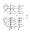
- Figure 1 shows schematically a small portion of a matrix (an “array") of "flotox" ("floating gate, tunnel oxide) memory cells of an EEPROM memory containing four bytes identified by the addresses (X1, Y1), (X1, Y2), (X2, Y1) and (X2, Y2), respectively.
- the array is organized in rows, two of which WL(X1) and WL(X2) are shown in the drawing.
- the rows can be selected individually by means of a conventional row-address decoding and selection circuit, not shown.
- the generic row drives selection transistors ST each of which is arranged in series with a respective memory cell MC, on the drain side thereof, and by means of which the memory cells MC are connected to a respective column or bit line BL.
- Each byte also comprises a byte-selection transistor BS (a "byte switch"), also driven by the row which drives the selection transistors ST arranged in series with the memory cells MC; the control gate CG common to all of the memory cells MC of the byte can be selected by means of the transistor BS in order to bring the necessary reading, writing or erasing voltages to the control gate CG.
- Each byte comprises a group of memory cells (connected to columns identified DB) for storing the datum, and a group of memory cells (two in the embodiment shown, connected to columns identified SB) for storing the status information.
- FIG. 2 shows schematically a small portion of an array of cells of a page-flash memory formed as described in European patent application No. 00830553.4 , already mentioned.
- each unitary memory element is constituted by a single floating-gate MOS transistor MC arranged in a row (a word line) which also constitutes its control gate.
- the drains of the memory cells MC belonging to the same column or bit line BL are electrically connected to the bit line, permitting selective programming by the injection of hot electrons into the floating gate, selecting a row (WL(X1), WL(X2), WL(Xn) and a column BL.
- the ability to write and erase the memory with a resolution of one byte is achieved by the provision of a plurality of p-type semiconductor wells PW ("p-wells"), separated from one another and each having a width (in the direction in which the rows extend) such as to house, for each row, the number of cells necessary to make up a byte with the respective cells for storing the status information (eight memory cells for storing the datum and, in the embodiment shown, two memory cells for storing the status information).
- the same row thus extends through a plurality of wells PW.
- the elemental memory unit which can be written and erased selectively is given by the set of cells of the same row which lie in the same well PW.
- the pairs of physical bytes may be obtained simply with the use of one of the bits which make up the row or column address, in dependence on the implementation selected; the need to provide a correlation table is thus avoided.
- the pairs of bytes may belong to adjacent rows (in which case the row addresses X1 and X2 differ in the least significant bit) or may belong to two rows the addresses X1 and X2 of which differ in the most significant bit (that is, two rows belonging to different halves of the array of memory cells).
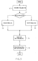
- Figures 3 and 4 are flow charts of two possible algorithms for the reading of a memory according to the present invention.
- the algorithm of Figure 3 provides for two consecutive readings to be performed in sequence: in the example shown, the byte (X1, Y1) is read first (box 30) and the content of the status word associated with the byte (X1, Y1) is then evaluated (box 31). If the byte (X1, Y1) is the active byte, its content is output (box 32). Otherwise, the byte (X2, Y2) is read (box 33) and its content is output (box 34).
- the reading access time it is possible to perform both readings every time, irrespective of whether or not the first byte read is the active byte.
- the result of the reading performed first is kept temporarily, for example, in a volatile memory register, whilst the second reading is performed.
- This makes it possible, amongst other things, to check the status words associated with both of the physical bytes.
- the physical byte the content of which is to be output is selected on the basis of the contents of the two status words, by simple combinatory logic.
- this second algorithm clearly has a considerable advantage in terms of the access time for reading the memory.
- Figures 5 , 6 and 7 show, in terms of flow charts, three possible algorithms for the writing of a new datum.
- the algorithm provides for the reading (box 50) of the contents of the two physical bytes.
- the contents of the two status words associated with the two physical bytes read is then checked (box 51) to establish which of them is active and which is non-active.
- the new datum is then written (boxes 52, 53) in the non-active byte.
- the status words associated with the two physical bytes are updated (box 54) so as to set the byte which was previously non-active as active. Finally, the non-active byte is erased (box 55).
- the sequence for changing the byte to be considered as active can be rendered completely safe only by updating the status words in a completely controlled manner so that, even if a malfunction were to occur between the updating of the status word associated with one of the two physical bytes and the updating of the status word associated with the other physical byte there would be no ambiguity as to which of the two physical bytes were to be considered active.
- Figure 6 shows the flow chart of an algorithm for the writing of a new datum which enables the desired safety to be achieved.
- the contents of the two physical bytes (X1, Y1) and (X2, Y2) have been read (box 60)
- the contents of the respective status words are checked to establish which of the two physical bytes is active (box 61).
- the new datum is then written in the non-active byte (box 62 or box 63) and the status word associated with that byte is set.
- the previously active physical byte is then erased (box 64 or box 65). After this, the status word of the previously non-active byte is set again to confirm that it has become active (box 66 or box 67).
- Figure 6A shows the sequence of changes in the status words of the two bytes (X1, Y1), and (X2, Y2), in tabular form.
- the initial state is assumed to be that identified (a) in the table, in which the status word associated with the byte (X1, Y1) is "11" (to signify that the byte is non-active), whilst the status word associated with the byte (X2, Y2) is "00" (byte active).
- the status word of the byte (X1, Y1) is then brought to "11" (state (f)), possibly during the erasure of the content of the byte (X1, Y1). Finally, it is confirmed that the byte (X2, Y2) is active by bringing its status word to "00" (state (g) in Figure 6A ).
- the example given above relates to the case of a page-flash memory in which it is possible to achieve, selectively, a writing operation, that is, a transition from the "1" state to the "0" state, even of a single bit (writing by hot electrons which brings about an increase in the threshold voltage of the memory cell).
- a writing operation that is, a transition from the "1" state to the "0" state
- the states will be the inverse of those described since, in a memory of this type, the operation which can be performed even at the level of a single bit is the extraction of electrons from the floating gate of the memory cell by the tunnel effect, that is, a transition from the "0" state to the "1" state.
- the information contained in the two status words, concerning which of the two bytes is to be considered active, is thus sure to be updated without the risk of error, for example, owing to a loss of supply voltage; there is in fact no time interval between the updating of the content of one status word and the updating of the content of the other status word.
- the algorithm of Figure 7 provides for a reading of the contents of the two physical bytes (X1, Y1), (X2, Y2) and of the respective status words to be performed (box 70). On the basis of the information contained in the respective status words, it is then established (box 71) which of the two bytes is active and which is non-active. The new datum is then written (box 72 or box 73) in the non-active byte and, simultaneously, the contents of the status words of the two bytes are updated; the byte which was previously active thus becomes non-active whilst the byte which was previously non-active becomes active. The byte which is no longer active is then erased (box 74 or box 75).
- Figure 7A shows the sequence of changes in the status words of the two bytes (X1, Y1) and X2, Y2), in tabular form.
- the initial state is assumed to be that indicated (a) in the table, in which the active byte is (X2, Y2); the status word associated with the byte (X1, Y1) is "11" (to signify that the byte is erased, that is, non-active), and the status word associated with the byte (X2, Y2) is "10" (byte active).
- the status word associated therewith is modified to "01”
- the status word associated with the byte (X2, Y2) is modified to "00" (box 72 in Figure 7 ).
- the resulting state is that indicated (b) in Figure 7A , which identifies the byte (X1, Y1) as active.
- the byte (X2, Y2) and the respective status word are then erased (box 74 of Figure 7 ) and the state indicated (c) in Figure 7A is reached, identifying the byte (X1, Y1) as active again, whilst the byte (X2, Y2) is identified as non-active.
- the status word thereof is set at "10" and, simultaneously, the least significant bit of the status word of the byte (X1, Y1) is written so that it becomes "00" (state (d) in Figure 7A ); the byte (X2, Y2) has thus become active.
- Figures 8 to 11 relate to further possible embodiments of the present invention.
- Figure 8 is a basic diagram of a flash memory which comprises two two-dimensional arrangements (or “arrays", as they will be referred to below) CORE1, CORE2 of memory cells of the non-volatile type which can be written and erased electrically.
- the memory cells are arranged in rows and in columns.
- the two arrays CORE1, CORE2 are substantially identical to one another and each of them comprises, in particular, a plurality of rows of memory cells; in Figure 8 , a row ROWm of the array CORE1, and a row ROWm of the array CORE2 are shown schematically.
- each array CORE1, CORE2 has a respective row-selection circuit (ROWDEC) 11, 12 which receives and decodes row addresses ADD_ROW, the latter being portions of addresses ADD supplied to the memory from the exterior in order to address a memory word.
- RowDEC row-selection circuit
- the row-selection circuits 11, 12 can select a single row of cells in the respective array for each row address ADD_ROW, supplying to this row the appropriate voltages for reading, for erasing, or for programming the memory cells of the row.
- a row of cells thus constitutes the smallest set of memory cells which can be erased independently of the other memory cells of the array.
- Each row of the arrays CORE1, CORE2 contains a plurality of memory words for storing data words;
- Figure 8 shows schematically a word WORDn of the row ROWm of the array CORE1, and a corresponding word WORDn of the row ROWm of the array CORE2.
- the memory words may, for example, have eight bits (in which case they are bytes) or sixteen or thirty-two bits.
- the word WORDn of the row ROWm of the array CORE1 and the word WORDn of the row ROWm of the array CORE2 are physical memory locations or "physical words" having a function wholly analogous to that performed by the physical address bytes (X1, Y1) and (X2, Y2) referred to in the description of the previous embodiment relating to a page-flash memory.
- each row of the arrays CORE1, CORE2 comprises, in addition to the memory words intended for storing the data, a respective status word for storing information on the status of the row, as described above for the status words stored in the columns SB with reference to a page-flash memory.
- the status word of the row ROWn of the array CORE1 is indicated SW1,m and the status word of the row ROWm of the array CORE2 is indicated SW2,m.
- the status word of a row is constituted, for example, by one or more memory cells which form part of the row but do not belong to any of the memory words of the row that are intended for storing datum words.
- the status word of a generic row is formed by at least one memory cell of the row which is additional to the memory cells of the row that form the memory words.
- respective portions of the arrays CORE1, CORE2 containing the memory cells which form the status words of the respective rows are indicated SW.
- the additional memory cell or cells of each row which form the respective status word belong to one or more columns SW1, SW2 of memory cells distinct from the columns that contain the memory-word cells.
- respective word-selection circuits (COLDEC) 21, 22 are associated with each of the two arrays CORE1, CORE2.
- the word-selection circuits 21, 22 select a memory word from all of those belonging to a row selected by the row-selection circuits 11, 12.
- the word-selection circuits 21, 22 select groups of columns of the array CORE1, CORE2, in dependence on a column-address portion ADD_COL of the address ADD.
- the memory also comprises reading circuits ("sense amplifiers") SA for reading the memory cells which form the memory words.
- the reading circuits SA are common to and shared by the two arrays CORE1, CORE2, since they are provided with switches SEL1 which enable the reading circuits SA to be connected selectively to one or to the other of the two arrays CORE1, CORE2.
- the switches SEL1 enable inputs of the reading circuits SA to be connected selectively to outputs of the word-selection circuits 21, 22 of one or, alternatively, of the other of the two arrays CORE1, CORE2.
- the memory comprises further reading circuits, schematically indicated by a block SWS in Figure 8 , for reading the cells which make up the status words of the rows of the two arrays CORE1, CORE2.
- the reading circuits SWS receive as inputs the columns SW1, SW2 of the memory cells which form the status words of the rows.
- the status-word reading circuits of the block SWS control the switches SEL2, determining to which of the two arrays CORE1, CORE2 the reading circuits SA are to be assigned.
- Outputs RD of the reading circuits SA carry a word datum resulting from the reading of a memory word of the array CORE1 or, alternatively, of the array CORE2.
- the outputs RD are supplied to output driver circuits ("buffers") OBUF which drive input/output data terminals I/O of the memory, that are accessible from outside the memory.
- the memory also comprises a volatile memory register 3.
- the register 3 can store, although in volatile form, the contents of all of the memory words belonging to a row of the array CORE1 or of the array CORE2.
- the register 3 thus comprises a number of volatile memory locations equal to the number of memory words of a generic row of one of the two arrays, and each location of the register REG has the same size as a generic memory word of the memory.
- the outputs RD of the reading circuits SA are also supplied to the volatile memory register 3 which can thus be loaded with the contents of the memory words belonging to a generic row of the array CORE1 or of the array CORE2.
- FIG. 8 shows, by way of example, a location LOCn of the register 3 corresponding to the memory word WORDn of the generic row ROWm of the array CORE1 and of the array CORE2.
- the content of the volatile memory register 3 is supplied by a series of switches SEL2 to one or other of the two arrays CORE1, CORE2 for writing in a respective row of the preselected array.
- the switches SEL2 are controlled by the block SWS which comprises the circuits for reading the status words of the rows of the two arrays.
- the row-selection circuits 11, 12 select two rows ROWm, of which one belongs to the array CORE1 and the other to the array CORE2, and which share the same row address ADD_ROW.
- the selection of the rows ROWm involves the selection of the respective status words SW1,m, SW2,m.
- the reading circuits SWS read the information regarding the status of the two rows contained in the respective status words SW1,m and SW2,m. On the basis of the information contained in the status words SW1,m, SW2,m, information is obtained on the content of the row ROWm of the array CORE1 and of the corresponding row ROWm of the array CORE2; in particular, it is possible to establish which of the two rows contains updated data to be accessed in the event of reading access to the memory, or which of the two rows is erased.
- the contents of the two status words are interpreted by the reading circuits SWS in order to determine what actions to perform.
- Table 1 below gives, by way of example, the correlation between the contents of the status words SW1,m, SW2,m of a pair of rows ROWm selected in the two arrays CORE1, CORE2, and the significance attributed to this content by the reading circuits SWS.
- the status words of the memory rows are two-bit words.
- "0" identifies a low logic level
- "1" identifies a high logic level
- "X" identifies either a high or a low logic level, without distinction.
- the memory is to be accessed in reading mode in order to read the content of a word of the memory having an address ADD.
- the address ADD which is composed of a column-address portion ADD_COL and of a row-address portion ADD_ROW, is supplied to the memory.
- the address ADD identifies, in each of the two arrays CORE1, CORE2, a row ROWm and a memory word WORDn within the row.
- the memory performs the following procedure.
- Step 1 the contents of the two status words SW1, SW2 associated with the two rows ROWm selected are read by means of the reading circuits SWS.
- Table 1 SW1 SW2 Significance 00 X1
- the row of CORE1 contains non-updated data
- the row of CORE2 contains corrupt data X1 00
- the row of CORE1 contains corrupt data
- the row of CORE2 contains non-updated data 00
- the row of CORE1 contains non-updated data (to be erased
- the row of CORE2 contains updated data 10
- the row of CORE1 contains updated data
- the row of CORE2 contains non-updated data (to be erased) 01 X1
- Both of the rows contain corrupt data X1 01
- Both of the rows contain corrupt data 01
- the row of CORE1 contains corrupt data
- the row of CORE2 contains valid data 10 01
- the row of CORE1 contains valid data
- the row of CORE2 contains corrupt data 10 11
- the row of CORE1 contains valid
- Step 2 the reading circuits SWS cause the switches SEL1 to switch so as to connect the reading circuits SA to the array which contains the row which, on the basis of the information resulting from the reading of the contents of the two status words, contains the valid data or the updated data.
- the reading circuits SWS therefore cause the switches SEL1 to connect the data-reading circuits SA to the outputs of the word-selection circuits 21 associated with the array CORE1.
- Step 3 the reading circuits proceed to read the contents of the memory cells of the memory word WORDn belonging to the row ROWm of the array CORE1 which contains the valid data, or in any case the updated data.
- the datum word RD which has been read is made available at the input/output terminals I/O of the memory by means of the output buffer OBUF.
- An address ADD of the memory word to be modified composed of a row-address portion ADD_ROW and of a column-address portion ADD_COL, is supplied to the memory. This address identifies a pair of rows ROWm, one belonging to the two-dimensional array CORE1 and the other to the two-dimensional array CORE2, and within the two rows, two memory words WORDn.
- Step 1 the contents of the status words SW1,m, SW2,m associated with the two selected rows ROWm are read by means of the reading circuits SWS. It is assumed that: SW1,m SW2,m 11 10 that is, on the basis of Table 1, the row ROWm of the array CORE1 is erased and the row ROWm of the array CORE2 contains valid data.
- Step 2 the contents of all of the memory words which belong to the selected row ROWm of the array CORE2 are read by means of the reading circuits SA; the datum words read from the memory words of the row are stored in the locations of the volatile memory register 3.
- Step 3 after the contents of all of the memory words which belong to the selected row of the array CORE2 have been stored in the volatile memory register 3, the content of the volatile memory register 3 corresponding to the memory word of address ADD the content of which is to be modified is modified; the new datum word ND to be written in the memory word addressed is supplied to the memory from the exterior and is used to modify the content of the location of the volatile memory register 3 which corresponds to the location addressed.
- Step 4 the content of the status word SW2,m is modified in a manner such as to indicate that the row ROWm of the array CORE2 contains "non-updated data" so that, on the basis of Table 1: SW1,m SW2,m 11 00
- Step 5 the content of the volatile memory register 3 is written in the memory words of the row ROWm of the array CORE1, that is, the row of the array CORE1 which corresponds to the row ROWm of the array CORE2, the status word SW1,m of which contains "11", to signify that it is erased and ready to be written;
- Step 6 the content of the status word SW1,m associated with the row ROWm of the array CORE1 in the memory word of which the content of the volatile memory register 3 has been written is modified so as to indicate that the row ROWm of the array CORE1 contains "updated data"; according to Table 1: SW1,m SW2,m 10 00
- Step 7 the row ROWm of the array CORE2 the memory words of which contain the no-longer updated and now useless data is erased.
- the row ROWm of the array CORE2 is thus prepared for a possible next writing of new data resulting from a request to modify a memory word of the row ROWm of the array CORE1.
- the status word SW2,m associated therewith is modified so as to indicate that the row is erased, that is, according to Table 1: SW1,m SW2,m 10 11
- Step 6 does not necessarily have to be performed after Step 6, that is, immediately after the step of writing the new data and modifying the status word associated with the other row.
- Step 7 may in fact also be performed at a different moment.
- Figure 9 shows schematically a memory according to a variant of the embodiment of Figure 8 in which, in each of the two arrays CORE1, CORE2, the memory cells are organized in a plurality of memory sectors SEC.
- the structure of a generic sector SEC is shown in detail in Figure 10 .
- the sector SEC comprises a respective plurality of memory cells MC constituted by floating-gate MOS transistors.
- the memory cells MC are arranged in rows R and in columns C; all of the memory cells MC of the same row R have respective control gate electrodes connected to one another; all of the memory cells MC of a generic column C have respective drain electrodes D connected to one another. All of the source electrodes S of the memory cells MC of the sector are electrically connected to one another and to a common source line SL.
- a row-selection circuit (ROWDEC) 31 which receives and decodes row addresses ADD_ROW is provided and, for the selection of a group of columns C, there is a column-selection circuit (COLDEC) 32 which receives and decodes column addresses ADD_COL.
- RowDEC row-selection circuit
- COLDEC column-selection circuit
- Figure 11 shows a possible further practical embodiment of the present invention at the same schematic level as Figure 8 .
- respective reading circuits SA1, SA2 are associated with each of the two arrays CORE1, CORE2.
- the switches SEL1 controlled by the status-word reading circuits SWS can select whether to connect the outputs of the reading circuits SA1 or the outputs of the reading circuits SA2 to the output driver circuits OBUF.
- the embodiment of Figure 8 limits power consumption and the dimensions of the integrated circuit in terms of silicon area. However, this adversely affects speed of access to the memory, since the time required to read the content of a memory word is the sum of the time required to read the status words of the rows selected in the two arrays (by means of the reading circuits SWS), of the time required to switch the switches SEL1, and of the time required by the reading circuits SA to read the content of the memory word selected.
- the embodiment of Figure 11 is faster since, each time an address is supplied to the memory, the two memory words which belong to the two arrays CORE1, CORE2 are in any case read in parallel (by means of the respective reading circuits (SA1, SA2).
- the contents of the status words associated with the rows of the two arrays CORE1, CORE2 to which the two memory words belong are read in parallel by the reading circuits SWS, and the switches SEL1 are then switched so as to connect the reading circuits SA1 or the reading circuits SA2, according to the information contained in the status words, to the output driver circuits (and to the volatile memory register 3).
- Figures 8 to 11 of the present invention not only solve the problem of providing a non-volatile memory which can be erased and modified electrically both by writing and by erasure, in single bytes or words, and which ensures the preservation of the datum previously stored until the new datum has been written, but also provide an alternative solution to that of European patent application No. 00830553.4 cited in order to provide a flash memory the content of which can be modified in single bytes or, more generally, in single memory words.
- a number K of operations to modify the content of a generic memory word actually translates into K/2 operations to modify (erase and rewrite) the contents of the memory words of a row of CORE1, and K/2 operations to modify (erase and rewrite) the contents of the memory word of the corresponding row of CORE2.
- the number of additional memory cells to be provided in each physical byte in the embodiments of Figures 1 and 2 , or in each row of each of the two two-dimensional arrays in the embodiments of Figures 8 to 11 , in order to implement the status words depends, in the first place, on the various states which are to be discriminated; it also depends on the number of different programming levels provided for individual memory cells (clearly, if two possible programming levels are provided for in a cell, the cell will store a single information bit, whereas if, for example, four different programming levels are provided for, the individual cell will store two bits).
- status words constituted by one cell, or by several cells, belonging to the same row or to the same physical byte with which the status word is associated, this is not a limitation.
- the cells which constitute the status words of the physical bytes or of the rows of the two arrays could in fact be produced in the form of a two-dimensional array distinct from the array or from the two arrays which contain the memory cells for storing the data.
- a respective status word formed in whatever manner, which can contain information indicative of the status of the physical byte or of the memory row, in particular, whether the physical byte or the memory row contains updated data or not, or whether the data has been erased, so as to be able to determine which of the two physical bytes corresponding to the same user location, or which of the two rows selected, one in one of the two arrays and the other in the other, should be used to retrieve the datum word to be read and which should be used to write the modified datum word.
- the present invention is also applicable if it is desired to produce a flash memory of which only a portion enables a datum stored therein to be kept until the operation to modify that datum is completed, whilst the remaining portion is of conventional type, that is, provides for the erasure of the pre-existing datum and the writing of the new datum to take place in sequence.
- pairs of physical words or bytes for the same user location that is, two substantially identical arrays of cells such as the arrays CORE1, CORE2 of the foregoing description, will be provided only for the said portion of the memory.
Landscapes
- Read Only Memory (AREA)
Claims (17)
- Elektrischer veränderbarer nicht flüchtiger Halbleiterspeicher, umfassend:mehrere Benutzerspeicherplätze, welche einzeln von außerhalb des Speichers adressierbar sind, um die darin enthaltenen Daten zu lesen und zu verändern, wobei jeder Benutzerspeicherplatz eine entsprechende Speicheradresse aufweist und ein entsprechendes Paar physikalischer Speicherplätze ((X1, Y1), (Y2, Y2); WORDn) enthält, welche eingerichtet sind, alternativ die Funktionen eines aktiven Speicherplatzes und die eines nicht aktiven Speicherplatzes anzunehmen, wobei der aktive Speicherplatz ein vorher geschriebenes Datum enthält und der nicht aktive Speicherplatz für das Schreiben eines neuen Datums verfügbar ist, um das vorher geschriebene Datum zu ersetzen, sodass auf eine Anfrage, das vorherige Datum mit dem neuen Datum zu ersetzen, das vorherige Datum in dem Speicher gehalten wird, bis das neue Datum geschrieben worden ist,gekennzeichnet durch:wenigstens ein Statuswort (SB; SW1, m, SW2, m), das zu jeweils einem Paar von physikalischen Speicherplätzen gehört und Information enthält, die den Status des Paares von physikalischen Speicherplätzen angibt, undein zweidimensionales Array von Speicherzellen (MC), bei welchem jeder physikalische Speicherplatz eine Gruppe von Speicherzellen (DB) zum Speichern des Datums umfasst und eine Gruppe von Speicherzellen (SB) zum Speichern der Information, die den Status des physikalischen Speicherplatzes angibt.
- Speicher nach Anspruch 1, bei welchem das wenigstens eine Statuswort zwei Statuswörter umfasst, die zu dem einen und zu dem anderen der physikalischen Speicherplätze des Paares entsprechend gehören, wobei jedes der zwei Statuswörter in der Lage ist, Information zu enthalten, die den Status des entsprechenden physikalischen Speicherplatzes angibt.
- Speicher nach Anspruch 1, bei welchem das zweidimensionale Array von Speicherzellen (MC) in Reihen (WL(X1), WL(X2), WL(Xn)) und Spalten (BL) angeordnet ist und jeder physikalische Speicherplatz der Paare physikalische Speicherplätze einen entsprechenden Satz von Speicherzellen (MC) umfasst, wobei die Speicherzellen jedes Paares physikalische Speicherplätze zu derselben Reihe oder derselben Gruppe von Spalten (CLS(Y1), CLS(Y2)) des zweidimensionalen Arrays gehören.
- Speicher nach Anspruch 3, bei welchem der Satz von Speicherzellen des physikalischen Speicherplatzes die Gruppe von Speicherzellen (DB) zum Speichern des Datums umfasst und die Gruppe von Speicherzellen (SB) zum Speichern der Information, die den Status des physikalischen Speicherplatzes angibt.
- Speicher nach Anspruch 1, bei welchem das zweidimensionale Array von Speicherzellen ein erstes zweidimensionales Array (CORE1) von Speicherzellen umfasst, bei welchem die Zellen in Speicherblöcken (ROWm) gruppiert sind, welche unabhängig voneinander gelöscht werden können, wobei die Zellen jedes Speicherblockes mehrere Speicherwörter (WORDn) zum Speichern von Datumwörtern bilden, ein flüchtiges Speicherregister (3) zum Speichern einer Kopie der Inhalte der Speicherwörter eines Speicherblocks, der ein zu veränderndes Speicherwort enthält, ein zweites zweidimensionales Array (CORE2) von Speicherzellen, das im Wesentlichen zu dem ersten zweidimensionalen Array identisch ist, wobei es eine eins-zu-eins Übereinstimmung zwischen den Speicherblöcken (ROWm) des zweiten zweidimensionalen Arrays, welche unabhängig voneinander gelöscht werden können, und entsprechenden Speicherblöcken (ROWm) des ersten zweidimensionalen Arrays gibt, und bei welchem, auf eine Anfrage, ein Speicherwort (WORDn), das ein nicht-aktualisiertes Datumwort enthält, zu verändern, das entweder zu dem ersten oder dem zweiten zweidimensionalen Array gehört, der Inhalt von all diesen Speicherwörtern derselben Speicherblöcke und auch das Speicherwort, das verändert werden soll, in das flüchtige Speicherregister kopiert werden, wobei der Inhalt des flüchtigen Speicherregisters in Übereinstimmung mit einem neuen Datumwort (ND) verändert wird, wobei der veränderte Inhalt des flüchtigen Speicherregisters dann in die Speicherwörter eines entsprechenden Speicherblocks des anderen zweidimensionalen Arrays geschrieben wird, und derselbe Speicherblock nur gelöscht wird, nachdem das Schreiben des Inhaltes des flüchtigen Speicherregisters in den entsprechenden Block vollendet wurde.
- Speicher nach Anspruch 5, bei welchem die Speicherzellen Feldeffekttransistoren mit entsprechenden Steuerelektroden sind, wobei die Speicherblöcke Reihen von Speicherzellen sind, die ihre Steuerelektroden verbunden haben, und jeder der ersten und zweiten zweidimensionalen Arrays entsprechende zugehörige Reihenauswahl-Schaltkreise (11, 12; 31) zum Auswählen einer Reihe von Speicherzellen in jedem der zweidimensionalen Arrays (CORE1, CORE2) in Reaktion auf eine Adresse (ADD) hat, die an den Speicher entweder zum Lesen oder zum Ändern des Inhalts eines Speicherwortes geliefert wurde.
- Speicher nach Anspruch 6, ferner umfassend ein entsprechendes Statuswort (SW1, m, SW2, m) zum Halten von Information, die den Status der Reihe von Zellen betrifft, wobei dies operativ zu jeder Reihe von Speicherzellen des ersten und des zweiten zweidimensionalen Arrays (CORD1, CORE2) gehört ist.
- Speicher nach Anspruch 7, bei welchem das Statuswort (SW1, m, SW2, m) Information enthält, die angibt, ob die Speicherwörter (WORDn) der entsprechenden Reihe von Speicherzellen (ROWm) gelöscht sind, nicht aktualisierte Datumwörter enthalten oder aktualisierte Datumwörter enthalten.
- Speicher nach Anspruch 8, bei welchem jede Reihe von Zellen (ROWm) des ersten und des zweiten zweidimensionalen Arrays wenigstens eine weitere elektrisch löschbare und programmierbare Speicherzelle zum Speichern der Information umfasst, die den Status der Reihe der Zellen betrifft.
- Speicher nach Anspruch 9, bei welchem das Statuswort ein Zwei-Bit-Wort ist.
- Speicher nach Anspruch 8 oder Anspruch 9, ferner umfassend Statuswort-Lese-Schaltkreise (SWS) zum Lesen der Information, die in den Statuswörtern (SW1, m, SW2, m) enthalten ist, die zu den Reihen von Speicherzellen des ersten und zweiten zweidimensionalen Arrays (CORE1, CORE2) gehören, die durch die Reihenauswahl-Schaltkreise (11, 12; 31) in Reaktion auf eine Adresse (ADD) ausgewählt wurden, die an den Speicher geliefert wurde.
- Speicher nach Anspruch 11, bei welchem die Statuswort-Lese-Schaltkreise (SWS) die Information interpretieren, die in den Statuswörtem (SW1, m, SW2, m) enthalten sind, die zu den Reihen von Speicherzellen des ersten zweidimensionalen Arrays und des zweiten zweidimensionalen Arrays (CORE1, CORE2) gehören, welche durch die entsprechenden Reihenauswahl-Schaltkreise (11, 12) in Reaktion auf eine Adresse (ADD) ausgewählt wurden, die an den Speicher geliefert wurde, um zu ermitteln:(a) im Lesemodus, zu welcher der zwei ausgewählten Reihen das Speicherwort gehört, das das aktualisierte Datumwort enthält,(b) im Veränderungsmodus, zu welcher der zwei Reihen das Speicherwort gehört, das das nicht aktualisierte Datumwort enthält, und welche der zwei Reihen andererseits gelöscht wurde oder löschbar ist.
- Speicher nach Anspruch 12, ferner umfassend Datumwort-Lese-Schaltkreise (SA; SA1, SA2), zum Lesen der Datumwörter, die in den Speicherwörtern enthalten sind.
- Speicher nach Anspruch 13, bei welchem die Lese-Schaltkreise (SA) dem ersten und dem zweiten zweidimensionalen Array (CORE1, CORE2) gehören und von ihnen geteilt werden, und bei welchem Schaltkreise (SEL1) zum Verbinden der Lese-Schaltkreise mit einem oder mit dem anderen der zwei zweidimensionalen Arrays (CORE1, CORE2) bereitgestellt sind.
- Speicher nach Anspruch 13, bei welchem die Lese-Schaltkreise (SA1, SA2) erste Lese-Schaltkreise (SA1) umfassen, die zu dem ersten zweidimensionalen Array (CORE1) gehören, zweite Lese-Schaltkreise (SA2), die zu dem zweiten zweidimensionalen Array (CORE2) gehören, und Schaltkreise (SEL1), welche Ausgaben von den ersten und zweiten Lese-Schaltkreisen empfangen und als ihre Ausgabe die Ausgabe des ersten Lese-Schaltkreises und alternativ die Ausgabe des zweiten Lese-Schaltkreises liefern.
- Speicher nach Anspruch 14, bei welchem die Statuswort-Lese-Schaltkreise (SWS) die Schaltkreise (SEL1) veranlassen, die Datumwort-Lese-Schaltkreise (SA) mit dem zweidimensionalen Array zu verbinden, das die Reihe von Zellen enthält, welche, basierend auf der Information, die im entsprechenden Statuswort enthalten ist, das aktualisierte Datumwort, im Lesemodus, enthält, oder das alte Datumwort im Änderungsmodus.
- Speicher nach Anspruch 15, bei welchem die Statuswort-Lese-Schaltkreise (SWS) die Schaltkreise (SEL1) veranlassen, die Ausgabe der Lese-Schaltkreise auszugeben, die zu dem zweidimensionalen Array gehören, das die Reihe von Speicherzellen enthält, welche, basierend auf der Information, die in dem entsprechenden Statuswort enthalten ist, im Lesemodus das aktualisierte Datenwort enthalten oder im Änderungsmodus das alte Datenwort.
Priority Applications (3)
| Application Number | Priority Date | Filing Date | Title |
|---|---|---|---|
| DE60041823T DE60041823D1 (de) | 2000-12-29 | 2000-12-29 | Ein elektrisch modifizierbarer nichtflüchtiger Halbleiterspeicher der eingeschriebene Daten solange hält, bis ihre Neuprogrammierung abgeschlossen ist |
| EP00830878A EP1220229B1 (de) | 2000-12-29 | 2000-12-29 | Ein elektrisch modifizierbarer nichtflüchtiger Halbleiterspeicher der eingeschriebene Daten solange hält, bis ihre Neuprogrammierung abgeschlossen ist |
| US10/036,088 US6839818B2 (en) | 2000-12-29 | 2001-12-28 | Electrically modifiable, non-volatile, semiconductor memory which can keep a datum stored until an operation to modify the datum is completed |
Applications Claiming Priority (1)
| Application Number | Priority Date | Filing Date | Title |
|---|---|---|---|
| EP00830878A EP1220229B1 (de) | 2000-12-29 | 2000-12-29 | Ein elektrisch modifizierbarer nichtflüchtiger Halbleiterspeicher der eingeschriebene Daten solange hält, bis ihre Neuprogrammierung abgeschlossen ist |
Publications (2)
| Publication Number | Publication Date |
|---|---|
| EP1220229A1 EP1220229A1 (de) | 2002-07-03 |
| EP1220229B1 true EP1220229B1 (de) | 2009-03-18 |
Family
ID=8175626
Family Applications (1)
| Application Number | Title | Priority Date | Filing Date |
|---|---|---|---|
| EP00830878A Expired - Lifetime EP1220229B1 (de) | 2000-12-29 | 2000-12-29 | Ein elektrisch modifizierbarer nichtflüchtiger Halbleiterspeicher der eingeschriebene Daten solange hält, bis ihre Neuprogrammierung abgeschlossen ist |
Country Status (3)
| Country | Link |
|---|---|
| US (1) | US6839818B2 (de) |
| EP (1) | EP1220229B1 (de) |
| DE (1) | DE60041823D1 (de) |
Families Citing this family (8)
| Publication number | Priority date | Publication date | Assignee | Title |
|---|---|---|---|---|
| EP1376608A1 (de) * | 2002-06-28 | 2004-01-02 | Cp8 | Programmierverfahren in einem nichtflüchtigen Speicher und System zur Realisierung eines solchen Verfahrens |
| US7174440B2 (en) * | 2002-10-28 | 2007-02-06 | Sandisk Corporation | Method and apparatus for performing block caching in a non-volatile memory system |
| DE60314979T2 (de) * | 2003-04-11 | 2008-04-10 | Em Microelectronic-Marin S.A. | Verfahren zur Aktualisierung eines nichtflüchtigen Speichers |
| KR100645047B1 (ko) * | 2004-10-12 | 2006-11-10 | 삼성전자주식회사 | 불휘발성 메모리 장치 및 그것의 고속 프로그램 방법 |
| US7706183B2 (en) * | 2005-07-27 | 2010-04-27 | Spansion Llc | Read mode for flash memory |
| US7423915B2 (en) * | 2006-01-17 | 2008-09-09 | Spansion Llc | Random cache read using a double memory |
| US8796155B2 (en) | 2008-12-04 | 2014-08-05 | Micron Technology, Inc. | Methods of fabricating substrates |
| FR3095073B1 (fr) * | 2019-04-12 | 2021-03-12 | St Microelectronics Rousset | Codage de données sur bus série |
Family Cites Families (12)
| Publication number | Priority date | Publication date | Assignee | Title |
|---|---|---|---|---|
| US4922456A (en) * | 1988-04-29 | 1990-05-01 | Scientific-Atlanta, Inc. | Method of reducing wearout in a non-volatile memory with double buffer |
| GB2251102B (en) * | 1990-12-21 | 1995-03-15 | Sun Microsystems Inc | Translation lookaside buffer |
| US5463758A (en) * | 1993-08-02 | 1995-10-31 | International Business Machines Corporation | System and method for reducing seek time for read operations in mirrored DASD files |
| JP3507132B2 (ja) * | 1994-06-29 | 2004-03-15 | 株式会社日立製作所 | フラッシュメモリを用いた記憶装置およびその記憶制御方法 |
| DE4443065A1 (de) * | 1994-12-03 | 1996-06-05 | Bosch Gmbh Robert | Verfahren zur Programmierung eines elektrisch löschbaren, nichtflüchtigen Speichers in einem elektronischen Rechengerät sowie Steuergerät zur Verwendung bei dem Verfahren |
| US5896393A (en) * | 1996-05-23 | 1999-04-20 | Advanced Micro Devices, Inc. | Simplified file management scheme for flash memory |
| JP3344907B2 (ja) * | 1996-11-01 | 2002-11-18 | 富士通株式会社 | Raid装置及び論理ボリュームのアクセス制御方法 |
| US5963970A (en) * | 1996-12-20 | 1999-10-05 | Intel Corporation | Method and apparatus for tracking erase cycles utilizing active and inactive wear bar blocks having first and second count fields |
| JP3706703B2 (ja) * | 1996-12-27 | 2005-10-19 | ローム株式会社 | Icカード |
| JP2000057039A (ja) * | 1998-08-03 | 2000-02-25 | Canon Inc | アクセス制御方法及び装置及びファイルシステム及び情報処理装置 |
| US6219656B1 (en) | 1998-11-25 | 2001-04-17 | Schlumberger Resource Management Services, Inc. | Memory integrity for meters |
| US6412080B1 (en) * | 1999-02-23 | 2002-06-25 | Microsoft Corporation | Lightweight persistent storage system for flash memory devices |
-
2000
- 2000-12-29 EP EP00830878A patent/EP1220229B1/de not_active Expired - Lifetime
- 2000-12-29 DE DE60041823T patent/DE60041823D1/de not_active Expired - Lifetime
-
2001
- 2001-12-28 US US10/036,088 patent/US6839818B2/en not_active Expired - Fee Related
Also Published As
| Publication number | Publication date |
|---|---|
| US20020130334A1 (en) | 2002-09-19 |
| EP1220229A1 (de) | 2002-07-03 |
| US6839818B2 (en) | 2005-01-04 |
| DE60041823D1 (de) | 2009-04-30 |
Similar Documents
| Publication | Publication Date | Title |
|---|---|---|
| EP2564388B1 (de) | Nichtflüchtiger speicher und verfahren mit decodierung von kombinierten geraden/ungeraden verschachtelungsblöcken mit adaptierter wortzeilenaktivierungsschaltung | |
| CN102918599B (zh) | 具有基本程序序列和写中止检测的非易失性存储器和方法 | |
| KR100551646B1 (ko) | 페이지 복사 기능을 갖는 반도체 기억 장치 | |
| US8363468B2 (en) | Semiconductor memory device | |
| US8832360B2 (en) | Solid state storage device controller with expansion mode | |
| US7471575B2 (en) | Non-volatile memory and method with shared processing for an aggregate of read/write circuits | |
| US6891753B2 (en) | Highly compact non-volatile memory and method therefor with internal serial buses | |
| JP3730423B2 (ja) | 半導体記憶装置 | |
| US6108236A (en) | Smart card comprising integrated circuitry including EPROM and error check and correction system | |
| TWI570728B (zh) | 具有資料留存分隔區之快閃記憶體 | |
| JPH035995A (ja) | 不揮発性半導体記憶装置 | |
| US6937513B1 (en) | Integrated NAND and nor-type flash memory device and method of using the same | |
| CN107112044A (zh) | 多芯片双写入 | |
| KR960005355B1 (ko) | 불휘발성 반도체기억장치 및 이를 이용한 기억시스템 | |
| US5067111A (en) | Semiconductor memory device having a majority logic for determining data to be read out | |
| CN101167140A (zh) | 具有可在用于数据和用于纠错码之间进行切换的区间的存储器 | |
| EP1220229B1 (de) | Ein elektrisch modifizierbarer nichtflüchtiger Halbleiterspeicher der eingeschriebene Daten solange hält, bis ihre Neuprogrammierung abgeschlossen ist | |
| CN107507644A (zh) | 存储器装置及其操作方法 | |
| JP2008299918A (ja) | 不揮発性半導体記憶装置及びその不良ブロック置き換え方法 | |
| US6185128B1 (en) | Reference cell four-way switch for a simultaneous operation flash memory device | |
| EP1160795B1 (de) | Referenzzellenmatrixanordnung zum Datenlesen in einer nichtflüchtigen Speicheranordnung | |
| CN120690258A (zh) | 存储器系统及其操作方法、存储装置及其操作方法 | |
| US7532510B2 (en) | Flash memory device with sector access | |
| JP2007257748A (ja) | 不揮発性記憶装置 | |
| JP2006024342A (ja) | 不揮発性半導体記憶装置、不揮発性半導体記憶装置の書き込み方法、メモリカード及びicカード |
Legal Events
| Date | Code | Title | Description |
|---|---|---|---|
| PUAI | Public reference made under article 153(3) epc to a published international application that has entered the european phase |
Free format text: ORIGINAL CODE: 0009012 |
|
| AK | Designated contracting states |
Kind code of ref document: A1 Designated state(s): AT BE CH CY DE DK ES FI FR GB GR IE IT LI LU MC NL PT SE TR |
|
| AX | Request for extension of the european patent |
Free format text: AL;LT;LV;MK;RO;SI |
|
| 17P | Request for examination filed |
Effective date: 20021211 |
|
| AKX | Designation fees paid |
Designated state(s): DE FR GB IT |
|
| 17Q | First examination report despatched |
Effective date: 20071019 |
|
| GRAP | Despatch of communication of intention to grant a patent |
Free format text: ORIGINAL CODE: EPIDOSNIGR1 |
|
| GRAS | Grant fee paid |
Free format text: ORIGINAL CODE: EPIDOSNIGR3 |
|
| GRAA | (expected) grant |
Free format text: ORIGINAL CODE: 0009210 |
|
| AK | Designated contracting states |
Kind code of ref document: B1 Designated state(s): DE FR GB IT |
|
| REG | Reference to a national code |
Ref country code: GB Ref legal event code: FG4D |
|
| REF | Corresponds to: |
Ref document number: 60041823 Country of ref document: DE Date of ref document: 20090430 Kind code of ref document: P |
|
| PLBE | No opposition filed within time limit |
Free format text: ORIGINAL CODE: 0009261 |
|
| STAA | Information on the status of an ep patent application or granted ep patent |
Free format text: STATUS: NO OPPOSITION FILED WITHIN TIME LIMIT |
|
| 26N | No opposition filed |
Effective date: 20091221 |
|
| GBPC | Gb: european patent ceased through non-payment of renewal fee |
Effective date: 20091229 |
|
| REG | Reference to a national code |
Ref country code: FR Ref legal event code: ST Effective date: 20100831 |
|
| PG25 | Lapsed in a contracting state [announced via postgrant information from national office to epo] |
Ref country code: FR Free format text: LAPSE BECAUSE OF NON-PAYMENT OF DUE FEES Effective date: 20091231 |
|
| PG25 | Lapsed in a contracting state [announced via postgrant information from national office to epo] |
Ref country code: GB Free format text: LAPSE BECAUSE OF NON-PAYMENT OF DUE FEES Effective date: 20091229 |
|
| PG25 | Lapsed in a contracting state [announced via postgrant information from national office to epo] |
Ref country code: IT Free format text: LAPSE BECAUSE OF FAILURE TO SUBMIT A TRANSLATION OF THE DESCRIPTION OR TO PAY THE FEE WITHIN THE PRESCRIBED TIME-LIMIT Effective date: 20090318 |
|
| PGFP | Annual fee paid to national office [announced via postgrant information from national office to epo] |
Ref country code: DE Payment date: 20111221 Year of fee payment: 12 |
|
| REG | Reference to a national code |
Ref country code: DE Ref legal event code: R082 Ref document number: 60041823 Country of ref document: DE Representative=s name: SAMSON & PARTNER, PATENTANWAELTE, DE |
|
| REG | Reference to a national code |
Ref country code: DE Ref legal event code: R081 Ref document number: 60041823 Country of ref document: DE Owner name: MICRON TECHNOLOGY, INC., US Free format text: FORMER OWNER: STMICROELECTRONICS S.R.L., AGRATE BRIANZA, IT Effective date: 20130515 Ref country code: DE Ref legal event code: R082 Ref document number: 60041823 Country of ref document: DE Representative=s name: SAMSON & PARTNER, PATENTANWAELTE, DE Effective date: 20130515 |
|
| REG | Reference to a national code |
Ref country code: DE Ref legal event code: R119 Ref document number: 60041823 Country of ref document: DE Effective date: 20130702 |
|
| PG25 | Lapsed in a contracting state [announced via postgrant information from national office to epo] |
Ref country code: DE Free format text: LAPSE BECAUSE OF NON-PAYMENT OF DUE FEES Effective date: 20130702 |