EP1220309A1 - Herstellungsverfahren einer elektronischen Packungsanordnung - Google Patents
Herstellungsverfahren einer elektronischen Packungsanordnung Download PDFInfo
- Publication number
- EP1220309A1 EP1220309A1 EP00830854A EP00830854A EP1220309A1 EP 1220309 A1 EP1220309 A1 EP 1220309A1 EP 00830854 A EP00830854 A EP 00830854A EP 00830854 A EP00830854 A EP 00830854A EP 1220309 A1 EP1220309 A1 EP 1220309A1
- Authority
- EP
- European Patent Office
- Prior art keywords
- mold
- protective package
- electronic circuit
- elastically deformed
- membrane
- Prior art date
- Legal status (The legal status is an assumption and is not a legal conclusion. Google has not performed a legal analysis and makes no representation as to the accuracy of the status listed.)
- Withdrawn
Links
Images


Classifications
-
- H—ELECTRICITY
- H10—SEMICONDUCTOR DEVICES; ELECTRIC SOLID-STATE DEVICES NOT OTHERWISE PROVIDED FOR
- H10W—GENERIC PACKAGES, INTERCONNECTIONS, CONNECTORS OR OTHER CONSTRUCTIONAL DETAILS OF DEVICES COVERED BY CLASS H10
- H10W74/00—Encapsulations, e.g. protective coatings
- H10W74/01—Manufacture or treatment
- H10W74/016—Manufacture or treatment using moulds
-
- H—ELECTRICITY
- H10—SEMICONDUCTOR DEVICES; ELECTRIC SOLID-STATE DEVICES NOT OTHERWISE PROVIDED FOR
- H10W—GENERIC PACKAGES, INTERCONNECTIONS, CONNECTORS OR OTHER CONSTRUCTIONAL DETAILS OF DEVICES COVERED BY CLASS H10
- H10W72/00—Interconnections or connectors in packages
- H10W72/50—Bond wires
- H10W72/531—Shapes of wire connectors
- H10W72/536—Shapes of wire connectors the connected ends being ball-shaped
-
- H—ELECTRICITY
- H10—SEMICONDUCTOR DEVICES; ELECTRIC SOLID-STATE DEVICES NOT OTHERWISE PROVIDED FOR
- H10W—GENERIC PACKAGES, INTERCONNECTIONS, CONNECTORS OR OTHER CONSTRUCTIONAL DETAILS OF DEVICES COVERED BY CLASS H10
- H10W72/00—Interconnections or connectors in packages
- H10W72/50—Bond wires
- H10W72/531—Shapes of wire connectors
- H10W72/5363—Shapes of wire connectors the connected ends being wedge-shaped
-
- H—ELECTRICITY
- H10—SEMICONDUCTOR DEVICES; ELECTRIC SOLID-STATE DEVICES NOT OTHERWISE PROVIDED FOR
- H10W—GENERIC PACKAGES, INTERCONNECTIONS, CONNECTORS OR OTHER CONSTRUCTIONAL DETAILS OF DEVICES COVERED BY CLASS H10
- H10W72/00—Interconnections or connectors in packages
- H10W72/851—Dispositions of multiple connectors or interconnections
- H10W72/874—On different surfaces
- H10W72/884—Die-attach connectors and bond wires
-
- H—ELECTRICITY
- H10—SEMICONDUCTOR DEVICES; ELECTRIC SOLID-STATE DEVICES NOT OTHERWISE PROVIDED FOR
- H10W—GENERIC PACKAGES, INTERCONNECTIONS, CONNECTORS OR OTHER CONSTRUCTIONAL DETAILS OF DEVICES COVERED BY CLASS H10
- H10W74/00—Encapsulations, e.g. protective coatings
- H10W74/10—Encapsulations, e.g. protective coatings characterised by their shape or disposition
-
- H—ELECTRICITY
- H10—SEMICONDUCTOR DEVICES; ELECTRIC SOLID-STATE DEVICES NOT OTHERWISE PROVIDED FOR
- H10W—GENERIC PACKAGES, INTERCONNECTIONS, CONNECTORS OR OTHER CONSTRUCTIONAL DETAILS OF DEVICES COVERED BY CLASS H10
- H10W90/00—Package configurations
- H10W90/701—Package configurations characterised by the relative positions of pads or connectors relative to package parts
- H10W90/731—Package configurations characterised by the relative positions of pads or connectors relative to package parts of die-attach connectors
- H10W90/734—Package configurations characterised by the relative positions of pads or connectors relative to package parts of die-attach connectors between a chip and a stacked insulating package substrate, interposer or RDL
Definitions
- the present invention makes reference to a method for manufacturing a protective package of an electronic device, particularly of a pressure sensor of the optic type and similar ones.
- the invention makes reference to a method for forming a protective package made out of plastic material for an electronic circuit integrated on semiconductor and comprising an electronic circuit that can be at least partially activated from the outside of the protective package and that is to be encapsulated in its turn in said protective package.
- the invention particularly relates, but not exclusively, to a method for forming a protective package made out of plastic material, for an integrated electronic device of the type having a window to access the electronic device at least partially, and the following description is made with reference to this application field, with the only aim to simplify its explanation.
- a further drawback occurs when the electronic circuit is tilted on the clamp surface, as shown in figure 5.
- the method shows an unwelcome resin infiltration during the mold filling phase, and the electronic circuit surface, which is not perfectly parallel to the support, is damaged.
- the sprung clamp must be introduced into the mold as many times as many are the devices to be molded. All these inserts increase the possibility of having part of the resin filling the spaces between the mobile portions during the mold filling phase, thereby causing a jam or a yield reduction of the resin to be deposited on the integrated circuit surface.
- the technical problem at the basis of the present invention is the one of providing a method for manufacturing protective packages with window, presenting features such to overcome the manufacturing method drawbacks of the prior art.
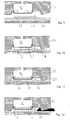
- a mold formed according to the invention is shown at 10, for obtaining a protective package 11a with a window.
- the mold 10 shows a space 11 containing the electronic circuit 13, for injecting an insulating material, for example resin.
- a lead frame 12 is placed, for example a metallic leaf, on a plastic substrate, a ceramic substrate, on which an electronic circuit 13 is fastened, comprising for example a proximity sensor, of the touch type or of the optic, pressure, fingerprints identification type, and similar.
- the following description makes reference to these types of sensor.
- the invention can obviously be applied to all the electronic devices that must have a surface portion in direct communication with the outside of the package, even though they are encapsulated in a protective package.
- the mold 10 comprises two half-parts: a half-mold, or lower half-shell 14, and a half-mold, or upper half-shell 15, which form a space 11 for containing the electronic circuit 13 when they are closed.
- the upper half-mold 12 has a lug which is formed of an element 17 made out of a material that can be elastically deformed, abutting in pressing contact against the electronic circuit 13.
- the upper half-mold 12 has a cavity 16 that is substantially delimited by the half-mold 12 and by the element 17, made out of a material that can be elastically deformed.
- the element 17 is an elastic membrane.
- Such membrane 17 is preferably made out of an elastomer.
- At least one portion of the cylindrical skirt 17a is maintained against the walls of the cavity 16.
- the cavity 16 is in communication with the outside of the mold through an opening 18.
- the cavity 16 is pressure filled trough the opening 18.
- the bottom 17b of the membrane perfectly adheres to the circuit 13 surface and abuts in pressing contact with said circuit.
- the integrated circuit 13 comprises for example a sensor which can be activated from the outside of the protective package 11a and connected to a control circuitry.
- the electronic circuit is connected to pins through thin conductor wires 19 for the outer electric connection.
- the lead frame 12 is positioned on the bottom of the molding cavity, and particularly in the hollow made by the lower half-mold 14.
- the lead frame 12 can also be placed in the middle of the containing space 11.
- the upper half-mold 15 is then laid upon the lower half-mold 14, so that a containing space 11 between the two half-molds is obtained, as shown in figure 10.
- the cavity 16 of the mold 10 delimited by the membrane 17, is filled with a pressure fluid at a predetermined value.
- the fluid pressure is then regulated at a suitable value.
- the fluid pressure inside the cavity 16 is higher than the pressure at which the resin is injected in the mold for forming the package of plastic material.
- the best results are obtained at a fluid pressure in the field from 60 to 70 Mpa.
- the pressure of the fluid applied to the membrane 17 allows the bottom 17b of the membrane to abut in pressing contact against the surface of the circuit 13 which has to be exposed, guaranteeing its seal from infiltrations.
- a surface of the bottom 17b is stressed by the pressing force, while the opposite surface of the bottom 17b is in pressing contact against the electronic circuit 13, leaving the entire boarder of the electronic circuit uncovered. In such a way the protective package will completely cover the circuit 13 border.
- the membrane 17 can cover also a side of the electronic circuit 13. In this way, the protective package of the invention will cover only the circuit 13 border which is left free from the membrane 17.
- the phase of forming the protective package 11a is carried out.
- a molten plastic material for example an epoxy resin at high temperature, is pressure injected in the cavity made between the half-molds through an injection opening 20 and through suitable channels that are not represented.
- the presence of the membrane 17 is such that it becomes a barrier to the stream of insulating material during the injection.
- the final protective package is then provided with a window or hole aligned with the integrated circuit 13.
- the method of the invention avoids the direct contact of metallic parts against the active part of the integrated circuit 13.
- a further advantage of the method according to the invention overcomes any possible misalignment of the integrated circuit 13, due for example to the faulty planarity of the substrate or of the surface of the integrated circuit, with the presence of the flexible membrane.
- inventive mold allows a greater number of packages to be formed, compared to the number of packages formed according to the prior art, and allows to use manufacturing processes with improved tolerances.
- inventive mold allows to simplify the formation of the mold, by removing all its mobile mechanical parts.
- the mold and the method according to the invention it is possible to adapt the intensity of the pressing contact against the integrated circuit from time to time during the production, thereby regulating the fluid pressure.
Landscapes
- Encapsulation Of And Coatings For Semiconductor Or Solid State Devices (AREA)
- Measuring Fluid Pressure (AREA)
- Injection Moulding Of Plastics Or The Like (AREA)
- Structures Or Materials For Encapsulating Or Coating Semiconductor Devices Or Solid State Devices (AREA)
Priority Applications (4)
| Application Number | Priority Date | Filing Date | Title |
|---|---|---|---|
| EP00830854A EP1220309A1 (de) | 2000-12-28 | 2000-12-28 | Herstellungsverfahren einer elektronischen Packungsanordnung |
| US10/036,335 US6811738B2 (en) | 2000-12-28 | 2001-12-26 | Manufacturing method of an electronic device package |
| JP2001401896A JP4109866B2 (ja) | 2000-12-28 | 2001-12-28 | 保護パッケージ形成方法および保護パッケージ成形用モールド |
| US10/961,489 US7238014B2 (en) | 2000-12-28 | 2004-10-08 | Manufacturing method of an electronic device package |
Applications Claiming Priority (1)
| Application Number | Priority Date | Filing Date | Title |
|---|---|---|---|
| EP00830854A EP1220309A1 (de) | 2000-12-28 | 2000-12-28 | Herstellungsverfahren einer elektronischen Packungsanordnung |
Publications (1)
| Publication Number | Publication Date |
|---|---|
| EP1220309A1 true EP1220309A1 (de) | 2002-07-03 |
Family
ID=8175608
Family Applications (1)
| Application Number | Title | Priority Date | Filing Date |
|---|---|---|---|
| EP00830854A Withdrawn EP1220309A1 (de) | 2000-12-28 | 2000-12-28 | Herstellungsverfahren einer elektronischen Packungsanordnung |
Country Status (3)
| Country | Link |
|---|---|
| US (2) | US6811738B2 (de) |
| EP (1) | EP1220309A1 (de) |
| JP (1) | JP4109866B2 (de) |
Cited By (11)
| Publication number | Priority date | Publication date | Assignee | Title |
|---|---|---|---|---|
| WO2003028086A1 (en) * | 2001-09-26 | 2003-04-03 | European Semiconductor Assembly (Eurasem) B.V. | Method for encapsulating a chip and/or other article |
| NL1024248C2 (nl) * | 2003-09-09 | 2005-03-10 | Fico Bv | Werkwijze en inrichting voor het met behulp van een flexibel drukelement omhullen van elektronische componenten. |
| WO2005071732A1 (en) * | 2004-01-22 | 2005-08-04 | Fico B.V. | Carrier for electronic components and methods for encapsulating and separating an electronic component |
| EP1276143A3 (de) * | 2001-07-09 | 2006-04-05 | ASM Technology Singapore Pte Ltd. | Giessform |
| EP1699089A1 (de) * | 2005-03-03 | 2006-09-06 | ATMEL Germany GmbH | Verfahren und Giessform zur Herstellung eines optischen Halbleitermoduls |
| DE102006016173A1 (de) * | 2006-04-06 | 2007-10-11 | Rohwedder Ag Micro Technologies-Werk Bruchsal | Abstützung von Substraten beim Spritzguss- und Spritzpressprozess (Transfer-Moulding) |
| EP2154713A1 (de) * | 2008-08-11 | 2010-02-17 | Sensirion AG | Verfahren zur Herstellung einer Messvorrichtung mit einer Spannungsverminderungsschicht |
| CN102218797A (zh) * | 2010-04-16 | 2011-10-19 | 华硕电脑股份有限公司 | 电子装置机壳及其制作方法 |
| WO2014116677A1 (en) * | 2013-01-23 | 2014-07-31 | Microchip Technology Incorporated | Open cavity plastic package |
| WO2016010425A1 (en) * | 2014-07-15 | 2016-01-21 | Sencio B.V. | Integrated circuit package moulding method and mould |
| WO2018098586A1 (en) | 2016-12-02 | 2018-06-07 | Mi Intégration S.E.N.C. | Apparatus and method for injection molding encapsulation |
Families Citing this family (28)
| Publication number | Priority date | Publication date | Assignee | Title |
|---|---|---|---|---|
| CN1224495C (zh) * | 2000-03-03 | 2005-10-26 | 快速科技有限公司 | 复合材料部件和金属部件的生产、成形、粘接、连接和修理系统 |
| TW564219B (en) * | 2001-01-25 | 2003-12-01 | Quickstep Technologies Pty Ltd | System and method for producing composite or bonded metal components |
| JP4874326B2 (ja) | 2005-03-22 | 2012-02-15 | クイックステップ、テクノロジーズ、プロプライエタリ、リミテッド | 複合材料管の製造 |
| US20080211145A1 (en) * | 2005-07-05 | 2008-09-04 | Quickstep Technologies Pty Ltd | Composite Component Production Using Fluid Density and Pressure |
| US7712213B2 (en) * | 2005-12-02 | 2010-05-11 | Aai Corporation | Angular encapsulation of tandem stacked printed circuit boards |
| JP2008066696A (ja) * | 2006-08-10 | 2008-03-21 | Denso Corp | 半導体製造装置および半導体製造方法 |
| KR101004087B1 (ko) * | 2008-10-27 | 2010-12-27 | 한국생산기술연구원 | 레이저를 이용한 이방전도성필름 패키징 장치 및 방법 |
| EP2224218B1 (de) * | 2009-02-25 | 2018-11-28 | Sensirion Automotive Solutions AG | Sensor in einer geformten Verpackung und Herstellungsverfahren dafür |
| US8646674B2 (en) | 2010-05-11 | 2014-02-11 | Ethicon Endo-Surgery, Inc. | Methods and apparatus for delivering tissue treatment compositions to stapled tissue |
| US8701267B2 (en) | 2010-11-05 | 2014-04-22 | Authentec, Inc. | Method of making a finger sensor package |
| CN103069556B (zh) * | 2010-12-27 | 2015-09-16 | 日产自动车株式会社 | 半导体模块、模制装置及模制成形方法 |
| US8729697B2 (en) * | 2012-01-09 | 2014-05-20 | Infineon Technologies Ag | Sensor arrangement, a measurement circuit, chip-packages and a method for forming a sensor arrangement |
| JP5708688B2 (ja) * | 2012-08-27 | 2015-04-30 | 株式会社デンソー | センサパッケージの製造方法 |
| NL2010252C2 (en) * | 2013-02-06 | 2014-08-07 | Boschman Tech Bv | Semiconductor product processing method, including a semiconductor product encapsulation method and a semiconductor product carrier-mounting method, and corresponding semiconductor product processing apparatus. |
| US9305894B2 (en) | 2013-06-05 | 2016-04-05 | Globalfoundries Inc. | Constrained die adhesion cure process |
| US9219051B2 (en) * | 2013-06-05 | 2015-12-22 | Globalfoundries Inc. | Laminate peripheral clamping to control microelectronic module BSM warpage |
| JP6166654B2 (ja) * | 2013-12-26 | 2017-07-19 | 矢崎総業株式会社 | 電子回路ユニットにおける外装ケースの成形方法 |
| JP5971270B2 (ja) * | 2014-02-27 | 2016-08-17 | トヨタ自動車株式会社 | 半導体装置の製造方法および製造装置 |
| CN104157936B (zh) * | 2014-07-29 | 2016-07-20 | 西南交通大学 | 基于半模基片集成波导的电可调谐带通滤波器 |
| NL2015091B1 (en) * | 2015-07-06 | 2017-01-30 | Besi Netherlands Bv | Mould, moulding press and method for encapsulating electronic components mounted on a carrier using elastomeric micro-pillars. |
| KR102652986B1 (ko) | 2019-03-07 | 2024-03-28 | 앱솔릭스 인코포레이티드 | 패키징 기판 및 이를 포함하는 반도체 장치 |
| JP7433318B2 (ja) | 2019-03-07 | 2024-02-19 | アブソリックス インコーポレイテッド | パッケージング基板及びこれを含む半導体装置 |
| JP7254930B2 (ja) | 2019-03-12 | 2023-04-10 | アブソリックス インコーポレイテッド | パッケージング基板及びこれを含む半導体装置 |
| EP3913662A4 (de) | 2019-03-12 | 2022-11-02 | Absolics Inc. | Verpackungssubstrat und verfahren zur herstellung davon |
| KR102396184B1 (ko) | 2019-03-12 | 2022-05-10 | 앱솔릭스 인코포레이티드 | 패키징 기판 및 이를 포함하는 반도체 장치 |
| US11981501B2 (en) | 2019-03-12 | 2024-05-14 | Absolics Inc. | Loading cassette for substrate including glass and substrate loading method to which same is applied |
| CN114678344B (zh) | 2019-03-29 | 2025-08-15 | 爱玻索立克公司 | 半导体用封装玻璃基板、半导体封装基板及半导体装置 |
| EP3905323B1 (de) | 2019-08-23 | 2024-08-14 | Absolics Inc. | Verpackungssubstrat und halbleiterbauelement damit |
Citations (4)
| Publication number | Priority date | Publication date | Assignee | Title |
|---|---|---|---|---|
| WO1987004973A1 (en) * | 1986-02-20 | 1987-08-27 | Libbey-Owens-Ford Co. | Seal construction for a mold structure for encapsulating glass with a gasket |
| US5275547A (en) * | 1992-01-03 | 1994-01-04 | Gencorp Inc. | Mold assembly with flexible membrane |
| EP0813236A1 (de) * | 1996-06-11 | 1997-12-17 | European Semiconductor Assembly (Eurasem) B.V. | Verfahren zum Einkapseln einer integrierten Halbleiterschaltung |
| JPH1075040A (ja) * | 1996-08-30 | 1998-03-17 | Toshiba Chem Corp | 樹脂被覆回路基板の製造方法 |
Family Cites Families (12)
| Publication number | Priority date | Publication date | Assignee | Title |
|---|---|---|---|---|
| SE461456B (sv) * | 1988-06-23 | 1990-02-19 | Ericsson Telefon Ab L M | Formverktyg |
| JPH05203522A (ja) * | 1992-01-23 | 1993-08-10 | Mitsubishi Electric Corp | モールドパッケージ半導体圧力センサおよびその製造方法 |
| WO1994016544A1 (fr) * | 1993-01-15 | 1994-07-21 | Vilyam Lazarevich Sanderov | Procede de production de microcircuits integres |
| KR970005706B1 (ko) * | 1994-01-24 | 1997-04-19 | 금성일렉트론 주식회사 | 고체촬상소자 및 그 제조방법 |
| SE514116C2 (sv) * | 1994-10-19 | 2001-01-08 | Ericsson Telefon Ab L M | Förfarande för framställning av en kapslad optokomponent, gjutform för kapsling av en optokomponent och tryckanordning för gjutform |
| US5929517A (en) * | 1994-12-29 | 1999-07-27 | Tessera, Inc. | Compliant integrated circuit package and method of fabricating the same |
| KR960043135A (ko) * | 1995-05-01 | 1996-12-23 | 엘리 웨이스 | 성형된 캡슐화 전자 구성요소 및 그의 제조 방법 |
| US5817545A (en) * | 1996-01-24 | 1998-10-06 | Cornell Research Foundation, Inc. | Pressurized underfill encapsulation of integrated circuits |
| US5956415A (en) * | 1996-01-26 | 1999-09-21 | Harris Corporation | Enhanced security fingerprint sensor package and related methods |
| US5997798A (en) * | 1997-06-27 | 1999-12-07 | International Business Machines Corporation | Biasing mold for integrated circuit chip assembly encapsulation |
| US5923959A (en) * | 1997-07-23 | 1999-07-13 | Micron Technology, Inc. | Ball grid array (BGA) encapsulation mold |
| WO2002015267A2 (en) * | 2000-08-17 | 2002-02-21 | Authentec Inc. | Integrated circuit package including opening exposing portion of an ic |
-
2000
- 2000-12-28 EP EP00830854A patent/EP1220309A1/de not_active Withdrawn
-
2001
- 2001-12-26 US US10/036,335 patent/US6811738B2/en not_active Expired - Lifetime
- 2001-12-28 JP JP2001401896A patent/JP4109866B2/ja not_active Expired - Fee Related
-
2004
- 2004-10-08 US US10/961,489 patent/US7238014B2/en not_active Expired - Lifetime
Patent Citations (4)
| Publication number | Priority date | Publication date | Assignee | Title |
|---|---|---|---|---|
| WO1987004973A1 (en) * | 1986-02-20 | 1987-08-27 | Libbey-Owens-Ford Co. | Seal construction for a mold structure for encapsulating glass with a gasket |
| US5275547A (en) * | 1992-01-03 | 1994-01-04 | Gencorp Inc. | Mold assembly with flexible membrane |
| EP0813236A1 (de) * | 1996-06-11 | 1997-12-17 | European Semiconductor Assembly (Eurasem) B.V. | Verfahren zum Einkapseln einer integrierten Halbleiterschaltung |
| JPH1075040A (ja) * | 1996-08-30 | 1998-03-17 | Toshiba Chem Corp | 樹脂被覆回路基板の製造方法 |
Non-Patent Citations (1)
| Title |
|---|
| PATENT ABSTRACTS OF JAPAN vol. 1998, no. 08 30 June 1998 (1998-06-30) * |
Cited By (25)
| Publication number | Priority date | Publication date | Assignee | Title |
|---|---|---|---|---|
| EP1276143A3 (de) * | 2001-07-09 | 2006-04-05 | ASM Technology Singapore Pte Ltd. | Giessform |
| US7205175B2 (en) | 2001-09-26 | 2007-04-17 | Elmos Advanced Packaging B.V. | Method for encapsulating a chip and/or other article |
| WO2003028086A1 (en) * | 2001-09-26 | 2003-04-03 | European Semiconductor Assembly (Eurasem) B.V. | Method for encapsulating a chip and/or other article |
| NL1024248C2 (nl) * | 2003-09-09 | 2005-03-10 | Fico Bv | Werkwijze en inrichting voor het met behulp van een flexibel drukelement omhullen van elektronische componenten. |
| WO2005043612A1 (en) * | 2003-09-09 | 2005-05-12 | Fico B.V. | Method and device for encapsulating electronic components using a flexible pressure element |
| CN1868048B (zh) * | 2003-09-09 | 2011-06-01 | 菲科公司 | 使用柔性压力元件来密封电子部件的方法和装置 |
| WO2005071732A1 (en) * | 2004-01-22 | 2005-08-04 | Fico B.V. | Carrier for electronic components and methods for encapsulating and separating an electronic component |
| US7740465B2 (en) | 2005-03-03 | 2010-06-22 | Atmel Automotive Gmbh | Casting mold for producing an optical semiconductor module |
| EP1699089A1 (de) * | 2005-03-03 | 2006-09-06 | ATMEL Germany GmbH | Verfahren und Giessform zur Herstellung eines optischen Halbleitermoduls |
| DE102006016173A1 (de) * | 2006-04-06 | 2007-10-11 | Rohwedder Ag Micro Technologies-Werk Bruchsal | Abstützung von Substraten beim Spritzguss- und Spritzpressprozess (Transfer-Moulding) |
| DE102006016173B4 (de) * | 2006-04-06 | 2008-01-17 | Rohwedder Ag Micro Technologies-Werk Bruchsal | Spritzgieß- oder Spritzpresswerkzeug |
| US7901971B2 (en) | 2008-08-11 | 2011-03-08 | Sensirion Ag | Method for manufacturing a sensor device with a stress relief layer |
| EP2154714A3 (de) * | 2008-08-11 | 2010-03-24 | Sensirion AG | Temperatursensor mit Pufferschicht |
| EP2154713A1 (de) * | 2008-08-11 | 2010-02-17 | Sensirion AG | Verfahren zur Herstellung einer Messvorrichtung mit einer Spannungsverminderungsschicht |
| CN102218797A (zh) * | 2010-04-16 | 2011-10-19 | 华硕电脑股份有限公司 | 电子装置机壳及其制作方法 |
| US9269597B2 (en) | 2013-01-23 | 2016-02-23 | Microchip Technology Incorporated | Open cavity plastic package |
| CN104969336A (zh) * | 2013-01-23 | 2015-10-07 | 密克罗奇普技术公司 | 开口腔体塑料封装 |
| WO2014116677A1 (en) * | 2013-01-23 | 2014-07-31 | Microchip Technology Incorporated | Open cavity plastic package |
| US9630352B2 (en) | 2013-01-23 | 2017-04-25 | Microchip Technology Incorporated | Open cavity plastic package |
| CN104969336B (zh) * | 2013-01-23 | 2019-02-01 | 密克罗奇普技术公司 | 开口腔体塑料封装 |
| WO2016010425A1 (en) * | 2014-07-15 | 2016-01-21 | Sencio B.V. | Integrated circuit package moulding method and mould |
| NL2013191B1 (en) * | 2014-07-15 | 2016-07-14 | Sencio B V | Integrated circuit package moulding method and mould. |
| WO2018098586A1 (en) | 2016-12-02 | 2018-06-07 | Mi Intégration S.E.N.C. | Apparatus and method for injection molding encapsulation |
| EP3548248A4 (de) * | 2016-12-02 | 2020-10-07 | MI Intégration S.E.N.C. | Vorrichtung und verfahren zum spritzgiessen von verkapselungen |
| US11130265B2 (en) | 2016-12-02 | 2021-09-28 | M.I. Integration S.E.N.C. | Apparatus and method for injection molding encapsulation |
Also Published As
| Publication number | Publication date |
|---|---|
| US20050085033A1 (en) | 2005-04-21 |
| US6811738B2 (en) | 2004-11-02 |
| JP4109866B2 (ja) | 2008-07-02 |
| US7238014B2 (en) | 2007-07-03 |
| JP2002261108A (ja) | 2002-09-13 |
| US20020093120A1 (en) | 2002-07-18 |
Similar Documents
| Publication | Publication Date | Title |
|---|---|---|
| US6811738B2 (en) | Manufacturing method of an electronic device package | |
| KR100320776B1 (ko) | 반도체장치의제조방법및수지밀봉장치 | |
| US6358773B1 (en) | Method of making substrate for use in forming image sensor package | |
| US7240847B2 (en) | Chip card | |
| US6254815B1 (en) | Molded packaging method for a sensing die having a pressure sensing diaphragm | |
| KR100241175B1 (ko) | 돌출부가 형성된 컬-블록을 갖는 트랜스퍼 몰딩 장치 | |
| US5733802A (en) | Semiconductor device and method of manufacturing the same | |
| JPH0590319A (ja) | 半導体デバイスを封止する方法および装置 | |
| KR20010012976A (ko) | 반도체 장치의 제조 방법, 반도체 장치의 몰드 장치 및반도체 장치 | |
| US7824958B2 (en) | Process and system for manufacturing an encapsulated semiconductor device | |
| EP1211721A1 (de) | Verbesserte elektronische Packungsanordnung und Herstellungsverfahren dafür | |
| KR20010049421A (ko) | 반도체소자를 캡슐화하기 위한 몰드조립 및 방법 | |
| JP3456983B2 (ja) | リードフレームおよび樹脂封止型半導体装置の製造方法 | |
| EP1211722A1 (de) | Herstellungsverfahren einer elektronischen Packungsanordnung | |
| CN100536100C (zh) | 电子元件的树脂密封成形装置 | |
| JPH05138691A (ja) | 液状樹脂射出成形金型 | |
| CN101017788A (zh) | 半导体装置的制造方法及半导体装置的制造装置 | |
| EP1259981B1 (de) | Anordnung und verfahren zum einkapseln elektronischer komponenten montiert auf einem träger | |
| JPS6154633A (ja) | 半導体樹脂封止用金型 | |
| KR19990029447A (ko) | 반도체 장치 및 그 제조 방법 | |
| KR100451382B1 (ko) | 플라스틱패키지의성형방법및그를성형하기위한반도체성형금형 | |
| US7723165B2 (en) | Method of forming component package | |
| CN1868048B (zh) | 使用柔性压力元件来密封电子部件的方法和装置 | |
| JP3602422B2 (ja) | 樹脂封止装置 | |
| JPH05243419A (ja) | Ppga用樹脂封止金型 |
Legal Events
| Date | Code | Title | Description |
|---|---|---|---|
| PUAI | Public reference made under article 153(3) epc to a published international application that has entered the european phase |
Free format text: ORIGINAL CODE: 0009012 |
|
| AK | Designated contracting states |
Kind code of ref document: A1 Designated state(s): AT BE CH CY DE DK ES FI FR GB GR IE IT LI LU MC NL PT SE TR |
|
| AX | Request for extension of the european patent |
Free format text: AL;LT;LV;MK;RO;SI |
|
| 17P | Request for examination filed |
Effective date: 20020919 |
|
| AKX | Designation fees paid |
Designated state(s): DE FR GB IT |
|
| STAA | Information on the status of an ep patent application or granted ep patent |
Free format text: STATUS: THE APPLICATION IS DEEMED TO BE WITHDRAWN |
|
| 18D | Application deemed to be withdrawn |
Effective date: 20080430 |